Digital Implementation of Phase Locked Loop on FPGA
Info: 10834 words (43 pages) Dissertation
Published: 23rd Dec 2021
Tagged: TechnologyElectronics
ABSTRACT
The report is based on the Digital Implementation of Phase locked loop on FPGA, the report covers the steps taken for implementing the proposed Phase Locked loop architecture on the FPGA. The building blocks used for the architecture are explained in detail as well as the software and technologies used for the project. An extensive literature research has also been done on past designs of the PLL and its contribution to this project is explained. Finally, the results gotten from the software and hardware will also be analysed.
TABLE OF CONTENTS
Click to expand Table of Contents
GLOSSARY
1. INTRODUCTION
1.1 AIMS AND OBJECTIVES
2. LITERATURE REVIEW
2.1. BUILDING BLOCKS OF PHASE LOCKED LOOP
2.1.1. PHASE DETECTOR
2.1.2. LOW PASS FILTER
2.1.3 VOLTAGE CONTROLLED OSCILLATOR
2.2. TYPES OF PHASE LOCKED LOOP
2.3. TECHNOLOGY AND DESIGN TOOLS
2.3.1. FPGA NANOBOARD
2.3.2. XILINX SYSTEM GENERATOR FOR DSP
2.4. FPGA BASED PLL BASED ON RANDOM SAMPLING
2.4.1. OVERVIEW
2.4.2. ARCHITECTURE OF PROPOSED DESIGN
2.4.3. IMPLEMENTATION OF EACH BLOCK
2.4.4. TESTING AND RESULTS
2.5. FPGA BASED PLL WITH WIRELESS TRANSCEIVER ARCHITECTURE TESTING
2.5.1. OVERVIEW
2.5.2. ARCHITECTURE OF PLL
2.5.3. IMPLEMENTATION
2.5.4. TESTING
2.5.5. ANALYSIS OF RESULTS
2.6. COMPARISON OF CASE STUDIES
2.7. CONTRIBUTIONS TO CURRENT WORK
2.8. NUMERICALLY CONTROLLED OSCILLATOR
2.8.1. OVERVIEW
2.8.2. CORDIC BASED NCO
2.8.3. IIR FILTER BASED NCO
2.8.4. LUT BASED NCO
3. SYSTEM DESIGN AND TESTING
3.1. OVERVIEW
3.2. PROPOSED SYSTEM ARCHITECTURE
3.2.1. PHASE DETECTOR
3.2.2. DIGITAL FILTER
3.2.3. NUMERICALLY CONTROLLED OSCILLATOR
3.3. TESTING OF EACH BLOCK
3.3.1. OVERVIEW
3.3.2. DIGITAL FILTER TEST
3.3.3. PHASE DETECTOR TEST
3.3.4. NUMERICALLY CONTROLLED OSCILLATOR TEST
4. RESULTS AND ANALYSIS
4.1. OVERVIEW
5. CONCLUSION
6. FURTHER DEVELOPMENT
REFERENCES
BIBLIOGRAPHY
APPENDIX A: PROPOSED PLL DESIGN
APPENDIX B: DIGITAL FILTER TEST DESIGN
APPENDIX C: PHASE DETECTOR TEST DESIGN
APPENDIX D: NUMERICALLY CONTROLLED OSCILLLATOR TIME DOMAIN TEST
LIST OF FIGURES
Figure 1: Basic Structure of Phase locked Loop
Figure 2: Xilinx FPGA
Figure 3: Design Flow for System generator for DSP
Figure 4: Logical Diagram of 16-Bit pseudo-random number generator
Figure 5: Fixed input frequency test, Output frequency (a, b, c) and LD signals for three different loop bandwidth [14].
Figure 6: Square Wave input frequency test. [14]
Figure 7: Sinusoidal input frequency test [14]
Figure 8: Simulink model of the ADPLL [12]
Figure 9: Proposed design of phase detector and loop filter
Figure 10: Simulated results of the ADPLL design[12].
Figure 11: Simulated Result for the NCO outputs I_feedback and Q_feedback [12].
Figure 12: The ADPLL set up [12].
Figure 13: I-Q constellation transmitted with the input signal of 2.4 GHz [12]
Figure 14: I-Q constellation recovered by the proposed ADPLL with the input signal of 2.4 GHz [12]
Figure 15: CORDIC Vector Rotation Diagram
Figure 16: 2nd order IIR Filter for generating sine wave
Figure 17: Block Diagram for LUT Based NCO[19].
Figure 18: Flow Chart describing whole project
Figure 19: Proposed Architecture of PLL
Figure 20: Response Curve for XOR Phase Detector [16].
Figure 21: Subsystem of Proposed NCO
Figure 22: Digital Filter test schematic
Figure 23: Output of Digital Filter with a 1Hz Input Signal
Figure 24: Phase Detector testing schematic
Figure 25: input signals with equivalent phases;
Figure 26: Difference in phase between the two input signals
Figure 27: Output of the PLL (Input Signal and Generated output signal)
Figure 28: Spectrum analyser view of the NCO output
LIST OF TABLES
Table 1: Parameter Values of Digital Filter
Table 2: Parameter values of two input signals
Table 3: Table Comparison between Input Signal and NCO output
GLOSSARY
| ABBREVIATION | MEANING |
| PLL | Phase Locked Loop |
| ADPLL | All-Digital Phase Locked Loop |
| VCO | Voltage Controlled Oscillator |
| MATLAB | Matrix Laboratory |
| FPGA | Field Programmable Gate Array |
| DSP | Digital Signal Processing |
| VHDL | VHSIC Hardware Description Language |
| RTL | Register Transfer Level |
| CDMA | Code Division Multiple Access |
| PI | Proportional Integrator |
| QPSK | Quadrature Phase Shift Keying |
| QAM | Quadrature Amplitude Modulation |
| BET | Bit Error Rate |
| NCO | Numerically Controlled Oscillator |
| ARS | Addictive Random Sampling |
| ADC | Analog to Digital Converter |
| DAC | Digital to Analog Converter |
| CORDIC | COordinate Rotation DIgital Computer |
| IIR | Infinite Impulse Response |
| DDS | Digital Design Synthesizer |
| FIR | Finite Impulse Response |
| LUT | Look-Up Table |
1. INTRODUCTION
Phase Locked loop is a control system which has an input signal that is synchronized in frequency and phase with a generated output signal gotten from a control oscillator. This means the PLL will be in a locked condition when the input signal and the output signal have zero or very small difference between there frequency and phase. Phase locked loop usually comprises of voltage controlled oscillator, phase detector or comparator and a low pass filter. The oscillator produces a periodic signal. The phase detector compares the phase of the input periodic signal with the phase of the produced/generated periodic signal and modifies the oscillator to keep the phases synchronized. The PLL is classified as a feedback loop system due to the fact that it takes an output signal towards the input signal for a comparison in a loop.
PLL’s are used in a variety of applications such as AM and FM Modulation, Frequency multiplication, Clock distribution and recovery and also jitter and noise reduction. They are also used in demodulating a signal, recovering a signal from a noisy communication channel and generate a stable frequency at multiples of an input frequency or distribute precisely timed clock pulses in digital logic circuits , for example a microprocessor [1].
1.1 AIMS AND OBJECTIVES
The sole aim of this project is to design a digitally based phased locked loop which can be implemented on an FPGA, the preferable type of PLL to use in this case is the All-Digital PLL which was discussed earlier. The reason being is due to the fact that all building blocks are digitally based. The aim of this report is to explain in details how the All-Digital PLL was modelled on Xilinx System Generator for DSP software and how it was eventually synthesized onto the FPGA. The project workload has been subdivided into various objectives which includes;
- Choosing the appropriate software
- Choosing the appropriate software blocks for the design
- Modelling the All-Digital Based PLL
- Setting the appropriate parameter units
- Testing the chosen software blocks
- Implementation and synthetisation of design on FPGA
2. LITERATURE REVIEW
An extensive literature research has been performed on the phase locked loop and it has been seen that its building blocks have various ways it could be implemented and also different digital and analog counterparts. This section will take an in-depth analysis of each of these blocks which will include the theory behind each of them, case studies, equations and diagrams etc. This section will also take an analysis of some related case studies and its contribution to the current project. An explanation on the devices required for the project have also been covered.
2.1. BUILDING BLOCKS OF PHASE LOCKED LOOP
The typical phase locked loop has three main building blocks in the design as stated in section 1. These blocks are mainly;
- Phase Detector
- Low pass Filter
- Voltage Controlled Oscillator
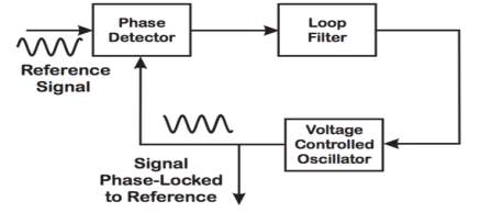
Figure 1: Basic Structure of Phase locked Loop
2.1.1. PHASE DETECTOR
This is the part of the PLL that is responsible for the comparing of the input signal and the generated output signal to determine whether or not both signals have similar phase and frequencies. This part of the PLL has the most significance due to the fact that is solely responsible for determining the phase difference in the loop and it also detects the resulting error in the PLL if there is any. In order for a better understanding of this block, assume there is a frequency of any random value, if the Fin≠ Fgen, the phase-error signal, after being filtered and amplified, causes the generated frequency to deviate in the direction of the of Fin[2]. If the conditions are right, the generated frequency will quickly lock to Fin, maintaining a fixed phase relationship with the input signal [2].
2.1.2 LOW PASS FILTER
This part of the PLL will remove unnecessary high frequencies which could pass out of the phase detector and go through the VCO. From Figure 1-1, it is seen that there is a reference signal in the block diagram which contains sum and difference frequency components which are often times called high and low frequency components respectively. The PLL will only require the high frequency components and it is the duty of the low pass filter to cut-off the low frequency components from the phase detector so the signal can be passed to the VCO. Thereafter, the input signal and reference signal will be locked in phase and frequency
2.1.3 VOLTAGE CONTROLLED OSCILLATOR
This block will feed the generated output signal to the phase detector to determine whether it is in phase with the input signal. The frequency of the output signal of the VCO is controlled by the input voltage driven into it. This input voltage will define the oscillation frequency. Consequently, modulated signals connected to the input signals may cause frequency modulation (FM) or phase modulation (PM). VCO can have a sine wave, square wave, ramp wave as its output but it’s solely dependent on the input signal driven into the phase locked loop. Analog based phase locked loop normally uses the VCO while the digitally based phase locked loop contains the VCO’s digital counterpart called a Numerically Controlled Oscillator (NCO) or in a semi-digital phase locked loop called a Digitally Controlled Oscillator (DCO).
2.2 TYPES OF PHASE LOCKED LOOP
There are different variations of the phase locked loop which can have either analogically or digitally based building blocks, these include;
- Digital PLL: Building blocks include an analog based VCO and low pass filter and a digital phase detector including XOR and Phase frequency detector
- Analog PLL: All analog based building blocks with a an analog multiplier used as the phase detector
- All-Digital PLL: All building blocks are digitally based and uses a numerically controlled oscillator (NCO) instead of a VCO.
- Software PLL: All blocks are implemented on a software rather than a hardware e.g. MATLAB
2.3 TECHNOLOGY AND DESIGN TOOLS
2.3.1 FPGA NANOBOARD
The term FPGA stands for Field Programmable Gate Array. An FPGA is an integrated circuit system which can be programmed or configured to the required functionality of the user. They are widely used in many industries for different purposes such as digital signal processing, media imaging, speech recognition, consumer electronics, military and aerospace. Due to these various applications this makes the FPGA more economical and marketable. Different companies such Xilinx Inc., Lattice Semiconductor and Altera Corporation are some of the top leading manufactures and accounted for more than 80% of the global FPGA market share in 2014[3].
The internal structure of an FPGA contains a programmable logic blocks such as AND & XOR, I/O cells which connects the logic cells to external signals and a programmable routing network interconnecting the cells. The FPGA are programmed using Hardware Description language such as Verilog and VHDL.
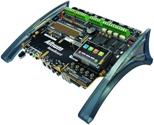
Figure 2: Xilinx FPGA
2.3.2 XILINX SYSTEM GENERATOR FOR DSP
System Generator is a DSP design tool from Xilinx that uses MathWorks model based Simulink design environment for FPGA design [7]. Past experience with Xilinx FPGA or RTL design approaches are not requires when utilizing system generator. Designers can develop and simulate a model using MATLAB, Simulink and Xilinx library of bit or cycle-true models. Xilinx pre-advanced algorithm are then mapped from the synthesizable hardware description language (HDL) which are made automatically from the tool. The HDL design will then be integrated for implementation on Xilinx FPGA and any other programmable SoCs. Subsequently, designers can characterize conceptual representation of a system-level design and effortlessly change this single source code into a gate level portrayal. Also, it gives a programmed generation of a HDL test bench, which can enable design to be verified after implementation. The figure below is a flow chart that summarizes the flow of a Simulink design to the implementation to the FPGA.
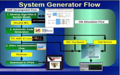
Figure 3: Design Flow for System generator for DSP
The level of abstraction given by System Generator for DSP has significantly clarified algorithm development. Besides the system-level modelling library, System generator incorporates a code generator that can automatically produces a synthesizable VHDL netlist from a Simulink model. This netlist contains IP (Intellectual property) that have been designed specifically for high level performance and density in Xilinx FPGA. System generator creates project and constraints file to assist implementation using Xilinx foundation as the major synthesis tool [11].
2.4. FPGA BASED PLL BASED ON RANDOM SAMPLING
2.4.1. OVERVIEW
It is well known that digitally based PLL are only compatible with low frequency based applications and cannot be processed with high frequency based applications. This is due to the fact that at high frequencies, there are a lot of mathematical calculations which restricts the functioning in a DSP system. Also the analog to digital converter (ADC) restricts the speed of DSP systems [4]. The proposed PLL based on random sampling is brought about by the idea of been able to use random sampling to process high frequency analog signals at frequencies lower than the Nyquist frequency without having an aliasing effect. Aliasing effect on a signal occurs when a signal is been sampled at a frequency similar or even smaller than the signal being measured.
2.4.2. ARCHITECTURE OF PROPOSED DESIGN
The PLL in this section follows the typical concept of a basic PLL were the components are the input signal, phase detector (PD), the loop filter, VCO and output signal. A sine wave is used as the input signal of the design. The phase detector generates a signal formed by the phase error which is added by other non-desired parts, for example, the high frequency harmonics originating from the non-linear components (i.e. multiplication) and arbitrary noise. The filter will sift out these redundant components and will just keep the phase error signal. The filter also functions as a controller in the closed loop system, which attempts to decrease the phase error signal to zero. The Proportional Integral (PI) is a good example of a filter that meets these necessities. The gain constants within the PI design can determine how far the locking time is and the range between each period of the output signal.
The sampling type methodology used in this design is called Addictive random sampling (ARS). This is a type of sampling methodology intended to provide alias-free processing of random signals [13]. The input signal driven into the phase detector of the proposed design is sampled at random moments which are characterised by the equation shown below;
| ti+1
= ti+ Ti |
(1) |
Where
tirepresents the sampling time and
Tiis the random period which is gotten based on the equation below;
Ti=(M
+
ri)×δ (2)
Where δ represents the time quantization which is defined by hardware limitation (the input clock in the present implementation) [14]. The variable r is a random whole number with a function given by;
f[r]
=
1R+1 with condition 0
≤r
≤R
Based on research, it is clearly seen that time quantization decides the peak frequency without the aliasing effect explained earlier. This frequency is significantly higher than the Nyquist frequency of the conventional sampling scheme. The product Mδ is the minimum sampling period, which relies on the DSP implementation speed and ADC conversion time. The random sampling scheme has the capability of diminishing the aliasing effect, if it utilized appropriately. Refer to the [1] and [2] in the bibliography as they give a detailed explanation of the methodology of this fact, which goes beyond the scope of the report.
2.4.3. IMPLEMENTATION OF EACH BLOCK
Random Period Generation
The random period generator unit for the architecture has two parts namely the pseudo-random number generation and the high speed programmable timer. Both of these parts can be executed efficiently using digital logic. The pseudo-random number (PN) generation is a typical task in a wireless communication applications, since it is able to generate codes in CDMA (Code Division Multiple Access). The architecture of current FPGA’s allows a proficient implementation of LSFR (Linear Shift Feedback Register). These registers can produce the Pseudo-random number as shown in the figure below;
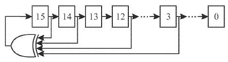
Figure 4: Logical Diagram of 16-Bit pseudo-random number generator
A sufficient feedback will assure a sequence with maximum period (
2n,where n represents the word size) [15].
Voltage Controlled Oscillator
This block in the architecture is implemented with a Direct Design Synthesizer (DDS). In order for the phase increment to be implemented, the VCO block must consider every sampling period of the filtered input signal. Therefore, the equation for the phase computation is given as shown below;
θi=θi-1+ ωTi
Where
θirepresents the phase accumulator,
ωrepresents the waveform frequency and
Tirepresents the sampling period. The VCO frequency is normally greater than the sampling frequency which means the phase increment will be greater than the maximum limit of the phase accumulator. The most significant bit of the phase increment are ignored, and the addition is computed only with the phase accumulator word size [14]. The eventual output of the VCO is then gotten by the use of a look-up table that will store each sample of the periodic sine wave. The Look-up table computes the each sample of the sine wave as follows;
pi=table[θi≫ SHIFT]
piin the equation is the output of the VCO and the condition
θi≫ SHIFTis what holds the sine table with a power of 2 number of elements [14]. The symbol >> shows a right shift.
Phase Detector
The phase detector in the design acts a scalar product, which will generate a nonlinear phase error. There are better phase detectors with direct phase response but with substantially higher computational expenses
PI Filter
The integrator of the proportional integrator (PI) filter is another operation with a sampling period that the architecture must consider. The equation below is used to calculate the integral term;
Ii=
Ii-1+ KITiei
The tem is similar to the equation used for uniform sampling;
Pi=
Kpei
The final equation for the PI filter the sum of the uniform sampling and the integral term;
PIi=
Ii+
Pi
Lock Detector
This part of the architecture is used to know the current condition of the PLL. The implemented Lock Detector is registered by the equation below;
LDi=qiin(ti)
Where
qirepresents the quadrature components (moved by 90º) of the VCO output
piand
LDirepresents the lock detector’s output signal. When the PLL is not in locked condition, the value of the DC equates to zero. Therefore, a low-pass filter (LPF) is used to filter-out the AC components and keep only the DC value. The implemented LPF is a first order IIR (infinite impulse response) filter, whose equation is given by [14].
yi
=
b0xi+ b1xi-1- a1yi-1
x and y represent the filter input at output signals and the constants a1, b0 and b1 are the filter coefficients[14]. The output of the lock detector is reliant on the input signal amplitude and the performance in its locked condition. The peak output of the filtered LD signal is 0.5 as long as it has an input signal with single phase amplitude. When the output of the PLL has frequency AC components, it is then modulated and will cause the signal of the LD to be changed. Therefore, the performance of the PLL locking time can be dependent on the LD signal level.
2.4.4. TESTING AND RESULTS
The testing of the proposed PLL architecture is done by driving the input with different input frequencies and analysing its impulse response (i.e. spectrum) and dynamic response. The output variables used to monitor the PLL are the output frequency and the LD signal. The LD signal level is used as an indicator of the PLL synchronization [14]. As mentioned in the earlier section, the constants PI is what will be used to classify the state of the PLL. The higher the value of the PI, the higher the bandwidth of the loop and the faster the locking time of the PLL will be.
The figure below shows the first test result of the design. In this test, an input frequency of 1MHz is driven into the PLL design with three different values of PI used individually on the design to show how they affected the values of the output frequencies and LD signals.
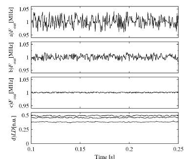
Figure 5: Fixed input frequency test, Output frequency (a, b, c) and LD signals for three different loop bandwidth [14].
The 2nd test will illustrate the dynamic response of the PLL. The figure 6 below shows the output signals of the PLL, plots (a) and (b) displays the response for a bandwidth with a low loop while plots (c) and (d) in the same figure shows the response to a bandwidth with a higher loop.
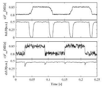
Figure 6: Square Wave input frequency test. [14]
The last plot in figure 6 above, represents the response of the PLL to a modulated input signal. The final test of the design uses a sinusoidal input signal with the 1st plot displaying the low loop bandwidth and the 2nd plot displays the high loop bandwidth.
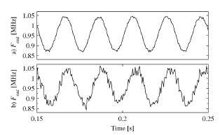
Figure 7: Sinusoidal input frequency test [14]
Based on all three tests, it is clearly seen that PLL is functioning properly. The PI is the main block responsible for the performance of the PLL as they determine the speed and the stability of the frequency.
2.5. FPGA BASED PLL WITH WIRELESS TRANSCEIVER ARCHITECTURE TESTING
2.5.1. OVERVIEW
The idea of testing an FPGA based PLL with wireless transceiver architecture was brought about with the idea to find a more feasible and cheaper way to implement a PLL purely in a digital domain to remove the phase as well as the frequency offsets at the baseband around zero carrier frequency. A clear literature has been done and it has been seen clearly that in order to implement a high speed and performance ADPLL, complex architectures and software based routines must be configured in the receivers at baseband frequencies [12]. This will need high cost Digital Signal Processors (DSP’s) and FPGA’s and thus bringing out this idea of implementing the designed PLL on a low cost reconfigurable FPGA which will be tested with wirelessly received signals.
2.5.2. ARCHITECTURE OF PLL
The architecture of the PLL consists of a mixer, phase detector, a loop filter and an NCO which follows the general principle of the PLL as discussed in section 1. It is designed on MATLAB Simulink as shown in the figure below;
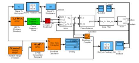
Figure 8: Simulink model of the ADPLL [12]
In the mixer and phase comparator, the input phase and the generated phased from the NCO are compared and an error signal is produced. The digital loop filter sends the average error signal to the NCO that will furthermore produce the desired frequency locked to the input signal. The figures below shows the time domain structures of both the phase detector and loop filter
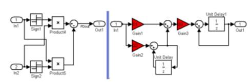
Figure 9: Proposed design of phase detector and loop filter
As seen from the figure above, there are two slicers in the phase detector sign1 and sign2, there function is simply to determine whether or not the next sample in the input has a negative and positive drift in phase when contrasted to the previous sample before it, with the differential phase error being its output. The output is then feed to the low pass filter, which will then calculate its average and produce a low pass filtered control signal which is based on its gain within the architecture. The gain of G1, G2 and G3 are 0.007813, 0.007813 and 0.015625[12].The gain are calculated based on the formula below
G=
K ɸ2N
The ADPLL model is intended to work for 200Ksps baseband IQ input signal i.e. QPSK only. QPSK is a type o phase shifting keying where two bits are modulated immediately, choosing one of four conceivable carrier phase shifts which are either 0, 90, 180 or 270 degrees. The design is then tested for a phase offset of 45 degree and frequency offset at 100Hz [12]. These values are ideal when trying to test the behaviour of an ADPLL locking performance. The figure below shows the simulated results of the ADPLL
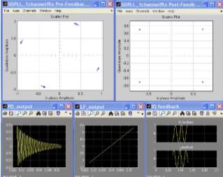
Figure 10: Simulated results of the ADPLL design[12].
In figure 12, the top left hand corner of the diagram displays the IQ constellation of the input signal. A constellation is a display of a modulated signal from a digitally based modulation plan, an example is a Quadrature Amplitude Modulation (QAM). From observing the IQ constellation graph. It doesn’t seem to be at a locked condition, it just rotating. On the other hand, the constellation of the output IQ signal which is on just next to the input constellation is seen to be at a fixed position and consequently at locked condition. Three graphs displayed at the bottom of figure 12 are damping out, loop filter output and the NCO stable cos and sin output. All these observed graphs have proven the ADPLL being in locked condition. Lastly, the bit error rate (BET) was discovered to be 0.1%, which meets the specifications for majority of wireless communication systems for data and voice transmission [12].
2.5.3. IMPLEMENTATION
In the implementation of the design, the fundamental functions like the data shift from left to right and vice versa in the registers and delaying a given data sample for a few known clock cycles in the top nodule Verilog file. Verilog code handles the mathematical calculations of all building blocks within the ADPLL request for sub-modules from outside of the top file. Thus, software engineers are given some flexibility in managing the mathematical operations for each of the building blocks within the PLL. All the basic mathematical operations are executed in the sub modules. Thusly, the ADPLL can be implemented easily in a low cost FPGA like Altera and Xilinx Spartan 7. Each block in the ADPLL is coded in Verilog language and it’s functional and time domain testing was done in ModelSim from Mentor graphics [12]. The figure 12 below shows a zoomed in view of the simulated result of the NCO outputs I_feedback and Q_feedback. It is seen clearly from figure 13 that the ADPLL is locking conditions with the input signal and the I_feedback and Q_feedback are seen to be sinusoidal waves as in the MATLAB simulated result in figure 12(i.e. the bottom right figure).
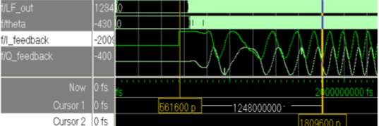
Figure 11: Simulated Result for the NCO outputs I_feedback and Q_feedback [12].
2.5.4. TESTING
As stated earlier in the overview section of 2.2, the designed ADPLL was tested using complete transceiver setup. A digital RF signal of 2.4GHz QPSK at 2.5Msps was transmitted using an Agilent Vector Signal Generator (VSG) as source with an Omni-directional monopole antenna [12]. In a wireless lab environment that consists of testing hardware’s, PCs, test benches at a distance of about 3m, the wireless signal was gotten components such as patch antenna, RF down-converter and an Analog to Digital converter (ADC). The data from the signal will then be processed with the designed ADPLL implemented on the FPGA. When the ADPLL is in its locked condition, there were 1020 samples of the processed data are stored and after that retransmitted through a DAC/RF up-converter which has a rate 16.272114Ksps.The eventual signal was received using a spectrum analyser and the IQ diagrams were plotted Agilent Vector Signal Analysis software.
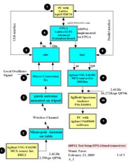
Figure 12: The ADPLL set up [12].
2.5.5. ANALYSIS OF RESULTS
The figures below shows the I-Q constellation of both the modulated signal received and the ADPLL design with its input signal 2.4 GHz as stated previously. Both figures are very similar in their features but with a few differences which are;
- In the ADPLL design, of the recovered data there were only 1020 of its samples were repeated again and again. The moment where data from the FPGA begins repeating a couple of samples does not make a complete symbol time span and consequently causes a scatter close to every symbol point in the quadratic constellation as in the figures
- The FPGA itself causes a few errors in the stored information/ data
- The settings of the measurement filters in VSA software are done as user defined type and reference filter as rectangular type in order to see a clear view of the constellation. In any case, these settings in fact have no effect on the reliability of the recovered data.
- Finally, the noise and contortion commitment from RF, ADC and DAC in the system model.
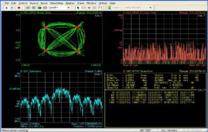
Figure 13: I-Q constellation transmitted with the input signal of 2.4 GHz [12]
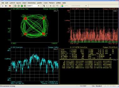
Figure 14: I-Q constellation recovered by the proposed ADPLL with the input signal of 2.4 GHz [12]
2.6. COMPARISON OF CASE STUDIES
After the research and comparison of the two studies, it can be seen that both designs are beneficial to the engineering industries of nowadays, as they are both implemented on low cost reconfigurable FPGA’s. Based on further analysis, it is clear that the FPGA based PLL with random sampling has more advantages over the wireless transceiver PLL, as high frequency analog signals can be implemented on PLL with random sampling and on a normal basis, FPGA based PLL can only transmit low frequency signals. This could also be useful to wireless communication industries that use high frequencies analog signals for network purposes. Also, the challenge of aliasing effect is rectified.
2.7. CONTRIBUTIONS TO CURRENT WORK
This research focused on past designs of phase locked loop implemented digitally and analogically and to prove why digitally based PLLs are superior to its analog counterpart. The PLL also aims to achieve better locking time. Subsequent to the testing of the proposed design, a conclusion will be made to decide the performance of the ADPLL and to find out what changes and improvement could be made for performance improvement.
2.8. NUMERICALLY CONTROLLED OSCILLATOR
2.8.1. OVERVIEW
In order to implement an All-Digital PLL onto an FPGA, only a numerically controlled oscillator must be used to feed the generated signal back to the phase detector as stated in Section 1.2.Therefore it is important to understand the theory behind the implementation of the NCO and this section will explain in detail how each implementation type is done. A numerically controlled oscillator, sometimes referred to as Direct Digital Synthesizer is a timer that uses the overflow of an accumulator to create an output signal [6]. The NCO which is the analog counterpart of the VCO has better advantages over any other type of controlled oscillator in terms of precision, dependability and reliability. The main purpose of an NCO is to generate either a sinusoidal or other periodic waveform The NCO has three different ways it can be implemented onto an FPGA and these include;
- CORDIC based NCO
- Look-Up Table based NCO
- IIR Filter Based NCO
2.8.2. CORDIC BASED NCO
CORDIC (Coordinate Rotation Digital Computer) which is also known as Volder’s algorithm is a basic and effective algorithm methodology used to calculate mathematical, trigonometric and hyperbolic functions in a cycle called binary search. The concept on CORDIC was brought about on the idea of rotating the period of a complex number, by multiplying it by a progression of constituent values. In any case, the multiplies can be a power of 2, so in binary arithmetic they can be done using just shifts and adds; no actual multiplier is needed[8]. Compared to other methodologies, CORDIC is the best way for software implementation or when hardware is not involved e.g. in a microcontroller or maybe when logic gates need to be saved to implement one e.g. FPGA. Then again, in a hardware implementation e.g. in a microprocessor, a Look-Up Table is a more preferred methodology because it is quite faster than CORDIC. The CORDIC algorithm is used in many areas of digital signal processing and communication systems which includes direct digital frequency synthesizer, digital modulation and direct cosine transform. The CORDIC algorithm simply means shifting a vectors x & y to a new vector x’ & y’ by an angle  as shown in the figure below;
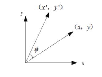
Figure 15: CORDIC Vector Rotation Diagram
As shown in Figure 9, the CORDIC algorithm implies changing a vector x and y into a different vector x’ and y’. The essential circular iteration (roundabout cycles) functions of CORDIC algorithm can be found in the formula below;
| X’ = x.cos – y.sin
Y’= y.cos |
(1) |
By collecting the like terms cosin both equations, the new equations are derived
| X’ = cos[x – y.tan]
Y’= cos |
(2) |
Assuming tan=
±2-i, where I represents the current iterative times 0 to N, therefore the iterative can be written as;
| Xi+1
= Ki[ xi-yi.di. 2-i] Yi+1 = Ki[ yi+xi.di. 2-i] |
(3) |
Where
di=
±1 and
Ki= cos (
tan-12-i) = 1/
1+2-2i
Eventually, when the iteration step function is sufficient enough, the variable
Ki= 0.6073. Therefore, the iteration equation should be multiplied by the gain which can be calculated by the equation below;
| An
= ∑i=1N1+2-2i |
(4) |
The resultant model of the revolution iteration which was utilized by the CORDIC algorithm is shown in equation 5
| Xi+1
= xi-yi.di. 2-i Yi+1 = yi+xi.di. 2-i Zi+1 = zi-di.tan-1(2-i) |
(5) |
With each progression of the rotation, the value
diis computed as a sign of the
zias seen in equation 6
| di
= -1 if zi di= 1 if zi>0 |
(6) |
Resultant is
| Xn
= An[ x0cosz0-y0.sin. z0] Yn = An[ y0cosz0+x0.sin. z0] Zn = 0 |
(7) |
The resultant after the vector
y0is initialised to 0 are shown is equation 8
| Xn
= Anx0cosz0 Yn = Any0cosz0 |
(8) |
If
x0is the input data of the digital down converter (DDC), the Xn and Yn computed by the NCO are the results of the mixing. When multipliers are not in use, the mixing data can be obtained, which will reduce the hardware resources [9].
2.8.3. IIR FILTER BASED NCO
IIR (Infinite Impulse Response) Filter is a kind of digital filter where every sample of output is the weighted entirety of the previous and current sample of input using all past samples; however, the weights of previous samples are an inverse function of the sample age, approaching zero for old samples. Compared to its counterpart FIR (Finite Impulse Response), the IIR filter is more sufficient because they have feedbacks in there implementation i.e. a recursion in the filter. Thus, the IIR filter has a much better frequency response over the FIR filter of the same order. Unlike FIR filter, the phase characteristics is not linear which can cause a problem to the systems which need phase linearity. For this reason, it is not ideal to use IIR filter in digital signal processing when the phase of the essence [10]. The IIR Filter is a proficient methodology to generate a sine waveform, which is why it can be used as an NCO. The poles of the IIR filter must be inside the unit circle on the z-plane in order to stabilise the waveform. A 2nd order IIR filter for generating a sine waveform is shown below
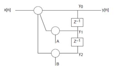
Figure 16: 2nd order IIR Filter for generating sine wave
2.8.4. LUT BASED NCO
Look up table (LUT) is a popular and generally preferred methodology used to generate a wave. This is because its concept is very basic and understandable and the programming is quick, due to it being under a digital environment. The methodology to this Look-Up Table is simply that it applies a phase to amplitude conversion strategy where pre-calculated coefficients of the sine/cosine wave are stored in a table, and are accessed through the use of a phase accumulator [18]. The structure of the look up table based NCO consists of the actual look up table which is sometimes called ROM, which contains the waveform data for one period of the output and a counter used for indexing into the table. “The rate of change of the counter determines the frequency of the output wave, in normalized units, because the output wave still exists in the discrete time domain“[19]. The counter is sometimes called a phase accumulator since it stores the present value of the sine waves phase and the sum it changes by for every period is called phase. In summary, the easiest way to clarify how the NCO works based on LUT is that it tracks the argument
sin(2πfn)in a counter and uses the look up table to calculate the corresponding value of
sin(2πfn)[19]. The figure below illustrates the block diagram for a LUT based NCO;
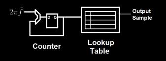
Figure 17: Block Diagram for LUT Based NCO[19].
3. SYSTEM DESIGN AND TESTING
3.1. OVERVIEW
This section will explain the entire flow of the project, from the design of the proposed architecture of the ADPLL to the eventual implementation of the design on the FPGA. The figure below shows the flow chart of how project will go through from the proposed architecture to software and hardware simulation and getting results.
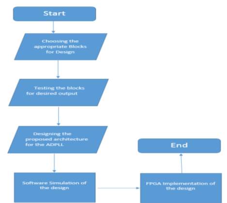
Figure 18: Flow Chart describing whole project
3.2. PROPOSED SYSTEM ARCHITECTURE
The figure below shows the overall architecture for the proposed PLL;
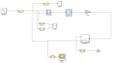
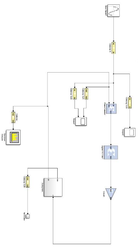
Figure 19: Proposed Architecture of PLL
In the above architecture the main building blocks that make up the design include multiplier (phase detector), FIR filter (Digital Filter), gain and NCO subsystem.
3.2.1. PHASE DETECTOR
1st Approach: Multiplier
The multiplier block is used as to act as the phase detector for the design, the multiplier is widely used for phase detection, especially in the analog based PLL for high frequencies. When the reference signal and the input signal are multiplied together, the sum and difference frequencies are generated. The difference frequencies are the desired frequencies needed for the output. In most cases, there are no problems with the multiplier as the phase detector, whether in the analog or digital version of the PLL. The only inception is if the phase of the generated output differs from the reference phase by a 90º shift. Refer to the 3rd reference in the bibliography section for more details on this.
2nd Approach: XOR Gate
XOR gate is another alternative to be used as a simple and effective phase detector. When an XOR gate receives the input signal and generated signal, the output signal is 0 for the condition of two equal signals, while for the condition of two unequal signals gives an output signal of 1. This operation is an ideal method for a phase detector. There are a few disadvantages with using this phase detector and they include;
- The waveform of both input and generated feedback signals are to have a 50% duty cycle i.e. 1:1. If this condition is not meet, the XOR gate will lock with a phase error.
- If the generated and input signal have different frequencies, the phase detector will have a tendency to jump between the regions of the gain [16]. The figure below shows the characteristic of the phase detector
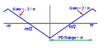
Figure 20: Response Curve for XOR Phase Detector [16].
- The ostensible locking point with an XOR phase detector is additionally at the 90º phase shift.
Due to problems with the XOR gate, the multiplier was chosen as the phase detector for the design.
3.2.2. DIGITAL FILTER
The Finite Impulse Response (FIR) filter is used as the low pass filter for the architecture. The FIR filters are the most commonly used filters implemented within a software and can implement most type of frequency responses digitally. Some of the major reason for it being used as low pass filters is because it promises a strict linear phase frequency characteristic with all sorts of amplitude frequency characteristics and also because the impulse response is finite, the FIR filters are stable system. The output of an FIR filter is generated when its input goes through a series of subsystem blocks namely delay, multiplier and adder. The two methods in implementing the FIR filter include;
Windowing Method
Windowing method is a simple and fast technique for designing FIR filters. This technique is based on discrete-time unlike other techniques which are designed in continuous time. The idea behind this technique is to choose frequency selective filters and then truncate its impulse response to create a casual linear phase based FIR filter [18].
Equiripple Method
An alternative methodology for generating an FIR filter is using the equiripple design. It generates more quality and proficient filters i.e. filters that only meet the specifications it is initialised. It also requires minimal number of coefficients.
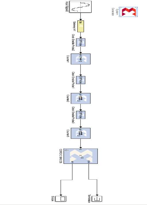
3.2.3. NUMERICALLY CONTROLLED OSCILLATOR
From Figure 19, it is seen that the NCO block is a subsystem, this subsystem contains step signals which counts one period of a sine wave from 0 to
2πand then
2πand –
2π. Then the CORDIC block will calculate the generated sine wave. The Simulink diagram for the subsystem of the NCO is as shown below;
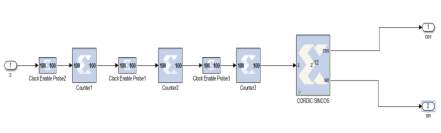
Figure 21: Subsystem of Proposed NCO
3.3. TESTING OF EACH BLOCK
3.3.1. OVERVIEW
This section will explain how the relevant building blocks of the phase locked loop will be tested in a separate Simulink file in order to get the desired output. This is done in order to determine the specific block that could bring about errors in the control system.
3.3.2. DIGITAL FILTER TEST
This section will cover the testing of the digital FIR filter. The figure below shows the Simulink diagram for the digital filter;
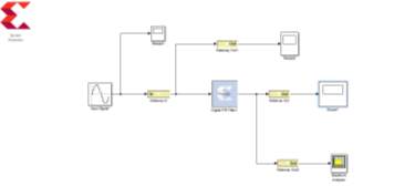
Figure 22: Digital Filter test schematic
The low pass filter is designed to pass all frequencies up to 20% of the Nyquist frequencies and will stop frequencies greater or equal to 50% of the Nyquist frequency. Nyquist frequency is the bandwidth signal and is equivalent to half of the input signal frequency. The filter is tested with an input signal 1Hz and the detailed parameters for the digital FIR filter are as shown in the table below;
| Parameter | Value |
| Design Methodology | Equiripple |
| Filter Order | Minimum Order |
| Units of Signal | Hz |
| Wstop | 20% |
| Wpass | 50% |
Table 1: Parameter Values of Digital Filter
The figure below shows the output of the digital filter after simulation;
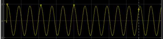
Figure 23: Output of Digital Filter with a 1Hz Input Signal
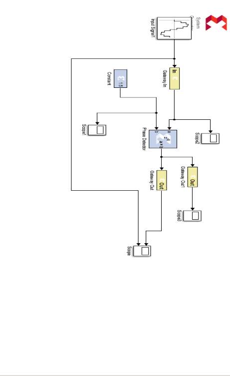
3.3.3. PHASE DETECTOR TEST
The section covers the testing of the phase detector i.e. the multiplier. The Simulink diagram for the phase detector with two input signals are shown below;
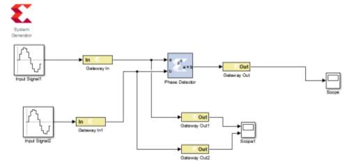
Figure 24: Phase Detector testing schematic
The parameters of the two input signals are as shown below;
| Parameters | Input Signal 1 | Input Signal 2 |
| Frequency(rad/s) | 1 | 1 |
| Amplitude | 2 | 1 |
| Phase(rad) | 1 | 1 |
Table 2: Parameter values of two input signals
After the simulation, it is has been analysed that the two are locked in phase as shown in the figure. Therefore, the phase detector is working as expected;
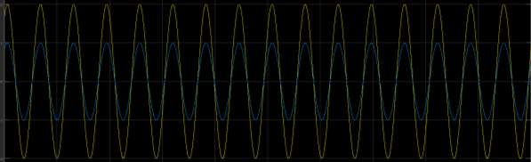
Figure 25: input signals with equivalent phases;
The figure is the output for the phase detector and it represents the difference in phase between the two input signals;
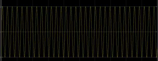
Figure 26: Difference in phase between the two input signals
4. RESULTS AND ANALYSIS
4.1. OVERVIEW
This section will discuss the simulated results from the software, and analyse the errors gotten. This Figure shows the output of the Phase locked loop after simulation of 100 seconds;
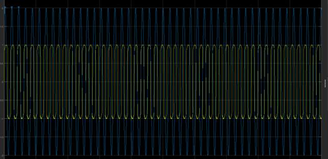
Figure 27: Output of the PLL (Input Signal and Generated output signal)
As seen from the figure 27, the two signals did not lock in phase and frequency. This is due to the failed NCO test. However, the generated signal and input signal is seen to be approximately in sync with each other. The table below shows that both signals are similar with regards to phase and frequency;
| PARAMETERS | INPUT SIGNAL | GENERATED SIGNAL |
| Frequency(Hz) | 461.540m | 488.043m |
| Period(sec) | 2.167 | 2.049 |
| +/- Duty Cycle | 50%/50% | 49.9%/50% |
| Amplitude | 2.000 | 1.009 |
Table 3: Table Comparison between Input Signal and NCO output
The spectrum analysis for the generated NCO output is as shown in the figure below;
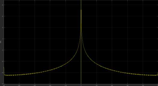
Figure 28: Spectrum analyser view of the NCO output
As seen from the figure above, the system is maximum at 0Hz and as the signal strength diminishes until before 500Hz on the positive and negative axis of the graph
5. CONCLUSION
This project presents an architecture for an ADPLL with different alternatives on how to implement the main building blocks. This project is implemented on the FPGA and modelled with the software Xilinx System Generator for DSP. The architecture was successfully modelled and follows the Phase Locked loop concept but the simulation results gotten were not expected. During the testing aspect of the project work, it was discovered that the Numerically Controlled Oscillator must be modelled with more than one block in order to generate the appropriate wave to the phase detector. The blocks used were the step function, phase accumulator and the clock probe.
Overall, the development of an All-Digital phase locked loop was interesting and also a good learning experience. There are still many improvements and concepts that still need to be researched and studied, but the fundamentals of an All-Digital PLL implementation on an FPGA was covered during the project.
6. FURTHER DEVELOPMENT
Considering the input signal and the generated signal didn’t have equal phase and frequency, the project can be improved by reconfiguring the Numerically Controlled Oscillator. This is because it was the NCO block that was responsible for the whole control system not functioning as expected. An in-depth background research must be done before trying to implement the NCO on Xilinx System generator for DSP and also a good knowledge of the software itself must be known. To summarise the operation of the NCO for a readers understanding, the main building blocks of an NCO include a clock source, increment block and a phase accumulator. Based on the literature review in section 2.8, there are different ways to implement an NCO on an FPGA. This knowledge will also be useful in order to configure the NCO for the proposed architecture for the PLL.
Also, there were intentions to have an application to the project which is frequency multiplication or synthesis. A frequency multiplier is a system for producing a series of frequencies from one single oscillator. In terms of designing this in the actual architecture design on System generator for DSP, the frequency multiplier block will generate multiple signals with the output of the NCO being its input. Refer to Appendix _ to view the proposed architecture for this application.
REFERENCES
Khan, T, Pooder, P, Khan, M and Rahman, M. (2014). FPGA IMPLEMENTATION OF PHASE LOCKED LOOP (PLL) WITH SYNCHRONOUS RESET. Available: http://iraj.in/up_proc/pdf/80-140118347971-74.pdf. Last accessed 14th April 2017.
Horowitz, P and Hill, W (1989). THE ART OF ELECTRONICS. 2nd ed. Cambridge: University Of Cambridge. p641.
Field Programmable Gate Array (FPGA) Market Size by Application (Data Processing, Industrial, Automotive, Consumer Electronics, Telecom, Military & Aerospace), Industry Analysis Report, Regional Outlo. Available: https://www.gminsights.com/industry-analysis/field-programmable-gate-array-fpga-market-size. Last accessed 3rd March 2017.
Sonnaillon, M and Bonetto,J. (2007). FPGA Implementation of a Phase Locked Loop Based on Random Sampling. Available: http://ieeexplore.ieee.org/stamp/stamp.jsp?arnumber=4234312. Last accessed 14th April 2017.
G. B. Lee, P. K. Chan and L. Siek, “A CMOS phase frequency detector for charge pump phase-locked loop,” 42nd Midwest Symposium on Circuits and Systems (Cat. No.99CH36356), Las Cruces, NM, 1999, pp. 601-604 vol. 2.
URL: http://ieeexplore.ieee.org/stamp/stamp.jsp?tp=&arnumber=867710&isnumber=18776
http://microchipdeveloper.com/8bit:nco.:Accessed on the 19th March 2017
https://www.xilinx.com/support/documentation/sw_manuals/xilinx11/sysgen_gs.pdfAccessed on the 20th March 2017
https://dspguru.com/dsp/faqs/cordic: Accessed on the 25th March 2017
Zhihua, L and Weilian,W. (2011). The Design of NCO based on CORDIC Algorithm and Implementation in FPGA. Available: http://ieeexplore.ieee.org/stamp/stamp.jsp?arnumber=6066683. Last accessed 4th April 2017.
https://learn.mikroe.com/ebooks/digitalfilterdesign/chapter/introduction-iir-filter/ Accessed on the 5th April 2017
Xilinx, Inc., DSP Design Flows in FPGA Tutorial Slides, 2003
M. A. Tarar, J. Sun, A. Sampson, R. Wilcox and Z. Chen. ). The Implementation of a New All-Digital Phase-Locked Loop on an FPGA and its Testing in a Complete Wireless Transceiver Architecture. http://ieeexplore.ieee.org/stamp/stamp.jsp?arnumber=4939132 (accessed 7th April 2017).
J.J. Wojtiuk. (2000). Randomised Sampling for Radio Design. Available: http://citeseerx.ist.psu.edu/viewdoc/download?doi=10.1.1.63.7938&rep=rep1&type=pdf. Last accessed 14th April 2017.
M.O. Sonnaillon, R. Urteaga and F. J. Bonetto, (2006). Random Sampling in High-Frequency Digital Lock-In Amplifiers”. Random Sampling in High-Frequency Digital Lock-In Amplifiers”. 36 (1), p181-186
G. Maria and P. Alfke. (2001). Linear Feedback Shift Registers in Virtex Devices. Linear Feedback Shift Registers in Virtex Devices. 1.2 (1), p1
Poole, I. PLL Phase Detector / Comparator. Available: http://www.radio-electronics.com/info/rf-technology-design/pll-synthesizers/phase-locked-loop-detector.php. Last accessed 16th April 2017.
Hinton, O. (2000). Chapter 4: Design of FIR Filters. Available: https://www.staff.ncl.ac.uk/oliver.hinton/eee305/Chapter4.pdf. Last accessed 16th April 2017
Salazar,A , Bahubalindruno, G,Locharla, Mendonça,H, Alves,J and J,Da Silva, . (2011). A Study on Look-up Table Based Sine Wave Generation. Available: http://paginas.fe.up.pt/~dee08011/files/Download/REC2011.pdf. Last accessed 16th April 2017.
(2011). Numerically Controlled Oscillators. Available: http://blog.thelonepole.com/2011/07/numerically-controlled-oscillators/. Last accessed 16th April 2017.
BIBLIOGRAPHY
M.O. Sonnaillon, R. Urteaga and F. J. Bonetto, (2006). Random Sampling in High-Frequency Digital Lock-In Amplifiers”. Random Sampling in High-Frequency Digital Lock-In Amplifiers”. 36 (1), p181-186.
J.J. Wojtiuk. (2000). Randomised Sampling for Radio Design. Available: http://citeseerx.ist.psu.edu/viewdoc/download?doi=10.1.1.63.7938&rep=rep1&type=pdf. Last accessed 14th April 2017.
Hagen, J. (1996). Phase Locked Loop. In: Radio-Frequency Electronics: Circuits and Applications. 2nd ed. Cambridge: University Of Cambridge. p136.
Afifiy,N, El Mone’m,S and Dahy,S. (2014). ALL Digital Phase Locked Loop (ADPLL) . Available: https://scholar.cu.edu.eg/?q=hmostafa/files/gp_2014_3.pdf. Last accessed 17th April 2017.
H, Dan. (2011). FPGA-based digital phase-locked loop analysis and implementation. Available: https://www.ideals.illinois.edu/bitstream/handle/2142/24165/Hu_Dan.pdf?sequence=1. Last accessed 17th April 2017.
APPENDICES
APPENDIX A: PROPOSED PLL DESIGN
APPENDIX B: DIGITAL FILTER TEST DESIGN
APPENDIX C: PHASE DETECTOR TEST DESIGN
APPENDIX D: NUMERICALLY CONTROLLED OSCILLLATOR TIME DOMAIN TEST
Cite This Work
To export a reference to this article please select a referencing stye below:
Related Services
View all


Related Content
All TagsContent relating to: "Electronics"
Electronics regards the science and technology involved in the development of electrical circuits and electronic devices and equipment that use them.
Related Articles

DMCA / Removal Request
If you are the original writer of this dissertation and no longer wish to have your work published on the UKDiss.com website then please: