Automatic Irrigation Water Supply Monitoring and Control
Info: 28927 words (116 pages) Dissertation
Published: 2nd Jun 2021
Tagged: Information SystemsTechnology
CHAPTER-1
Introduction
1.1 Embedded System:
An embedded system is an extraordinary reason framework in which the PC is totally typified by or committed to the gadget or framework it controls. Dissimilar to a broadly useful PC, for example, a PC, an inserted framework performs one or a couple predefined undertakings, for the most part with certain prerequisites. Since the framework is devoted to particular errands, outline architects can improve it, lessening the size and cost of the item. Installed frameworks are frequently mass-delivered, profiting by economies of scale.
Individual advanced aides (PDAs) or handheld PCs are for the most part viewed as implanted gadgets on account of the way of their equipment configuration, despite the fact that they are more expandable in programming terms. This line of definition keeps on obscuring as gadgets extend. With the presentation of the OQO Model 2 with the Windows XP working framework and ports, for example, a USB port — both elements more often than not have a place with “universally useful PCs”, — the line of classification foggy spots much more.
Physically, embedded systems ranges from versatile gadgets, for example, computerized watches and MP3 players, to substantial stationary establishments like activity lights, manufacturing plant controllers, or the frameworks controlling atomic power plants.
As far as many-sided quality inserted frameworks can go from extremely basic with a solitary microcontroller chip, to exceptionally complex with different units, peripherals and systems mounted inside a huge undercarriage or fenced in area.
Examples of Embedded Systems:
• Avionics, for example, inertial direction frameworks, flight control equipment/programming and other coordinated frameworks in air ship and rockets
• Cellular phones and phone switches
• Engine controllers and electronically monitored slowing mechanism controllers for vehicles
• Home mechanization items, for example, indoor regulators, aeration and cooling systems, sprinklers, and security observing frameworks
• Handheld number crunchers
• Handheld PCs
• Household apparatuses, including microwave broilers, clothes washers, TVs, DVD players and recorders
• Medical gear
• Personal advanced right hand
• Videogame comforts
• Computer peripherals, for example, switches and printers.
1.2 Block Diagram:
Section 1:
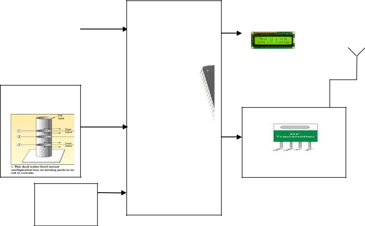
| 16×2 LCD | ||
| Power | ||
| Supply | MICRO | |
| CONTROLLER | ||
Water Level
Sensor
RF TX
SOIL
SENSOR
Fig:1.1 Block diagram of monitoring section
Controlling section:
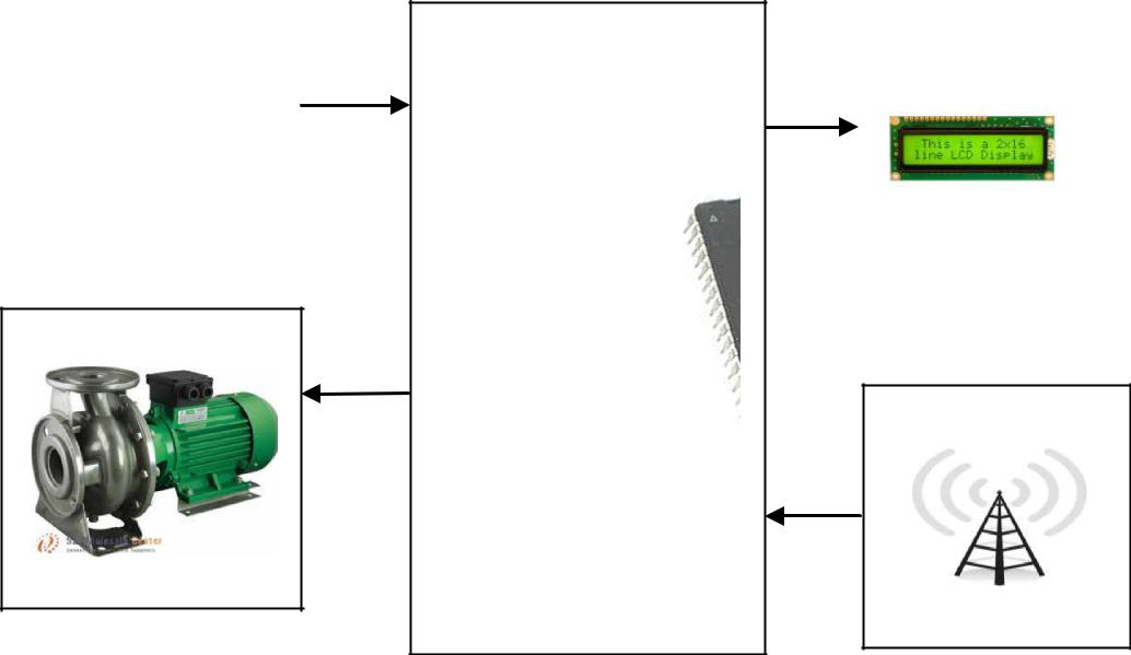
| Power | MICRO | 16×2 LCD |
| Supply | ||
| CONTROLLER | ||
Water Pump
RF RX
Fig:1.2 Block diagram of controlling section
1.3 Circuit Description:

Fig:1.3 circuit diagram of RF transmitter

Fig:1.4 circuit diagram of RF receiver
This section gives an overview of the whole circuitry and hardware involved in the project. The point of the project is to configuration minimal effort mobile phone based Embedded System for Irrigation.
In this project we are giving force supply to all units, The required working voltage for Microcontroller 89C51 is 5V. Consequently the 5V D.C. control supply is required by the same. This managed 5V is produced by venturing down the voltage from 230V to 18V utilizing venture down transformer. Presently the progression brought down a.c voltage is being corrected by the Bridge Rectifier utilizing 1N4007 diodes. The amended a.c voltage is presently sifted utilizing a ‗RC’ channel. Presently the corrected, sifted D.C. voltage is encouraged to the Voltage Regulator. This voltage controller gives/enables us to have a Regulated steady Voltage which is of +5V.The redressed; separated and directed voltage is again sifted for swells using an electrolytic capacitor 100μF. Now the output from this section is fed to
40th pin of 89c51 microcontroller to supply operating voltage. The microcontroller 89C51 with Pull up resistors at Port0 and crystal oscillator of 11.0592 MHz crystal in conjunction with couple of 30-33pf capacitors is placed at 18th& 19th pins of 89c51 to make it work (execute) properly. Operating voltage for the GSM modem will depends on its type and an adaptor is provided with the GSM modem set itself.
In this project we have two sections TRANSMITTER SECTION and RECEIVER SECTION. In the first section we have a water level sensor and a RF transmitter given to the micro controller Here water level sensors are used to sense the water level in the fields they are continuously monitor the water in fields and gives the information to the monitoring section based on that received information pumps will automatically on and off.
The other section is receiver section where If water is very less in fields that information is given through the transmitter section to the receiver section and the water pumps will on automatically otherwise off. Here we are using ar89s52 mc for controlling purpose and RF technology for wireless communication.
We are utilizing soil dampness sensor put at the plants to know how much water substance is available in the field
CHAPTER-2
Functional Description:
This Project mainly consists of Power Supply section, Microcontroller section,sensors, relay and LCD display section.
2.1 Power Supply Section:
This segment is implied for providing Power to every one of the areas specified above.It essentially comprises of a Transformer to venture down the 230V air conditioning to 18V air conditioning taken after by diodes. Herediodes are used to rectify the ac to dc. After rectification the obtained rippled dc is filtered using a capacitor Filter. A positive voltage regulator is used to regulate the obtained dc voltage.
2.2 Microcontroller Section:
This section forms the control unit of the whole project. This segment fundamentally comprises of a Microcontroller with its related hardware like Crystal with capacitors, Reset hardware, Pull up resistors (if necessary) etcetera. The Microcontroller forms the heart of the project because it controls the devices being interfaced and communicates with the devices according to the program being written.
2.3 Sensors:
Level Indicator:
Level indicator is used to indicate the different water levels in the tank or dam.
Soil Sensor:
Soil moisture sensors measure the water content in soil, the two copperleads act as the sensor probes. They are immersed into the specimen soil whose moisture content is under test.
2.4 Relay Section:
In this project relays are utilized to the Trip the parameters. A hand-off is an electrical switch that opens and closes under control of another electrical circuit. In the first frame, the switch is worked by an electromagnet to open or close one or many arrangements of contacts.
2.5 LCD Display Section:
This segment is essentially intended to show up the status of the venture. This venture makes utilization of Liquid Crystal Display to show/incite for essential data.
2.6 RF Transmitter:
In this project ST-TX01-ASK is used as the RF transmitter module. The encoded signal is given to the RF transmitters data pin. Then thesignal is modulated (ASK) by the RF transmitter module and transmitted through the antenna. This section is fully described in the RF communication section.
Circuit Diagram:
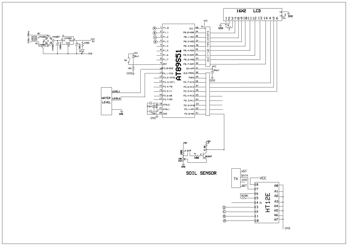
Fig:2.1RF transmitter internal diagram
2.6.1 Encoder:
We are using IC HT12E Encoder which is an 18 pin IC. This encoder circuit will encode the information send by the microcontroller and afterward transmits the information serially to the RF transmitter module. Here we are using ST-TX01 transmitter module for transmitting the data.
2.7 RF module (RECIEVER):
In this section we are using ST-RX04 RF Receiver module. The transmitted signal is received by this receiver module. The got information is transmitted to the decoder to decipher the information as we encoded the information while transmitting.
Circuit Diagram:
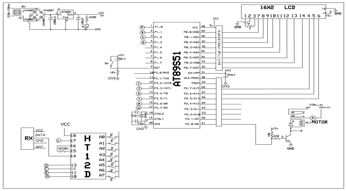
Fig:2.2RF receiver internal circuit diagram
2.8 Circuit diagram Explanation:
Firstly, the required working voltage for Microcontroller 89C51 is 5V. Thus the 5V D.C. control supply is required by the same. This regulated 5V is generated by first stepping down the 230V to 18V by the step down transformer. In the both the Power supplies the step downed a.c. voltage is being rectified by the Bridge Rectifier. The diodes used are 1N4007. The redressed a.c voltage is presently sifted utilizing a ‗C’ channel. Presently the amended, sifted D.C. voltage is encouraged to the Voltage Regulator. This voltage controller enables us to have a Regulated Voltage. In Power supply given to Microcontroller 5V is produced utilizing 7805. The redressed; separated and controlled voltage is again sifted for swells utilizing an electrolytic capacitor 100μF. Presently the yield from the main area is encouraged to 40th stick of 89c51 microcontroller to supply working voltage and from other power supply to transfer hardware.
The microcontroller 89c51 with Pull up resistors at Port0 and precious stone oscillator of 11.0592 MHz gem in conjunction with couple of capacitors of is put at 18th& nineteenth pins of 89c51 to make it work (execute) legitimately.
2.8.1 Micro Controller connections:
Pins Connections
9TH RESET
18th and 19th Crystal Oscillator circuit
20th Ground
40th VCC (+5V DC) supply
The LCD is interfaced to Microcontroller. The data pins of LCD are connected to Port 0. The control pins of LCD are connected to Port 2 as shown in schematic.
2.8.2 LCD connections to Micro controller:
| Pins | Connections |
| 1 | VSS (ground) |
| 2 | VCC (+5V) |
| 3 | 10k pot |
| 4 | RS, this pin is connected to P2.7 of the micro controller |
| 12 | |
| 5 | R/w, this pin is connected to P2.6 of the micro controller |
| 6 | EN, this pin is connected to P2.5 of the micro controller |
7-14 (D0-D7) these pins are connected to the port (P0) of the micro controller RF transmitter is connected to port 1 pin p1.0, p1.1, p1.2,p1.3
Water level sensor is given to port 3. P3.0 and p3.1.and soil sensor is given to p2.0
RF receiver is connected to port 1p1.0, p1.1, p1.2,p1.3. Relay is connected P2.0 to on & off the motor P2.0;
CHAPTER-3
Description of Micro Controller 89c51
3.1 Introduction
A Micro controller comprises of a capable CPU firmly combined with memory, different I/O interfaces, for example, serial port, parallel port clock or counter, intrude on controller, information securing interfaces-Analog to Digital converter, Digital to Analog converter, incorporated on to a solitary silicon chip.
In the event that a framework is produced with a microchip, the planner needs to go for outside memory, for example, RAM, ROM, EPROM and peripherals. Be that as it may, controller is given every one of these offices on a solitary chip. Improvement of a Micro controller lessens PCB size and cost of outline.
One of the real contrasts between a Microprocessor and a Micro controller is that a controller regularly manages bits not bytes as in this present reality application. Intel has presented a group of Micro controllers called the MCS-51.
The Major Features:
• Compatible with MCS-51 items
• 4k Bytes of in-framework Reprogrammable blaze memory
• Fully static operation: 0HZ to 24MHZ
• Three level programmable clock
• 128 * 8 –bit clock/counters
• Six interfere with sources
• Programmable serial channel
• Low control sit out of gear shut down modes.
- Why AT 89C51?
The framework prerequisites and control determinations plainly discount the utilization of 16, 32 or 64 bit small scale controllers or chip. Frameworks utilizing these might be prior to actualize because of huge number of inside elements. They are additionally speedier and more solid at the same time, 8-bit smaller scale controller acceptably serves the above application. Utilizing an economical 8-bit Microcontroller will fate the 32-bit item disappointment in any aggressive commercial center.
Going to the topic of why to utilize AT89C51 of all the 8-bit microcontroller accessible in the market the primary answer would be on account of it has 4 Kb on chip streak memory which is quite recently adequate for our application. The on-chip Flash ROM enables the program memory to be reconstructed in framework or by ordinary non-unpredictable memory Programmer. Besides ATMEL is the pioneer in glimmer innovation in today’s commercial center and thus utilizing AT 89C51 is the ideal arrangement.
3.3 AT89C51 Microcontroller Architecture:
The 89C51 engineering comprises of these particular components:
• Eight –bit CPU with registers A (the gatherer) and B
• Sixteen-bit program counter (PC) and information pointer (DPTR)
• Eight-bit stack pointer (PSW)
• Eight-bit stack pointer(Sp)
• Internal ROM or EPROM (8751) of 0(8031) to 4K (89C51)
• Internal RAM of 128 bytes:
1. Four enroll banks, each containing eight registers
2. Sixteen bytes, which possibly tended to at the bit level
3. Eighty bytes of universally useful information memory
• Thirty –two input/yield pins organized as four 8-bitport :p0-p3
• Two 16-bit clock/counters: T0 and T1
• Full duplex serial information beneficiary/transmitter:SBUF
• Control registers: TCON, TMOD, SCON, PCON, IP, and IE
• Two outer and three inside intrudes on sources.
• Oscillator and clock circuits.
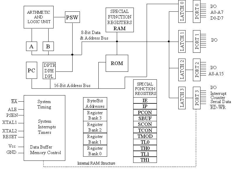
Fig :3.1Functional block diagram of micro controller
The 89C51 oscillator and clock:
The heart of the 89C51 hardware that creates the clock beats by which all the inner every single interior operation are synchronized. Pins XTAL1 And XTAL2 is accommodated interfacing a resounding system to frame an oscillator. Regularly a quartz precious stone and capacitors are utilized. The precious stone recurrence is the essential inner clock recurrence of the microcontroller. The makers make 89C51 plans that keep running at particular least and greatest frequencies regularly 1 to 16 MHz.
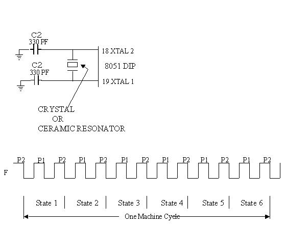
Fig 3.2: – Oscillator and timing circuit
Sorts of memory:
The 89C51 have three general sorts of memory. They are on-chip memory, outside Code memory and outer Ram. On-Chip memory alludes to physically existing memory on the small scale controller itself. Outer code memory is the code memory that dwells off chip. This is frequently as an outer EPROM. Outside RAM is the Ram that lives off chip. This regularly is as standard static RAM or glimmer RAM.
a) Code memory
Code memory is the memory that holds the real 89C51 projects that will be run. This memory is restricted to 64K. Code memory might be found on-chip or off-chip. It is conceivable to have 4K of code memory on-chip and 60K off chip memory all the while. In the event that lone off-chip memory is accessible then there can be 64K of off chip ROM. This is controlled by stick given as EA
b) Internal RAM
The 89C51 have a bank of 128 of inward RAM. The interior RAM is found on-chip. So it is the quickest Ram accessible. And furthermore it is most adaptable as far as perusing and composing. Interior Ram is unpredictable, so when 89C51 is reset, this memory is cleared. 128 bytes of inward memory are subdivided. The initial 32 bytes are partitioned into 4 enroll banks. Each bank contains 8 registers. Inner RAM likewise contains 128 bits, which are tended to from 20h to 2Fh. These bits are bit tended to i.e. every individual piece of a byte can be tended to by the client. They are numbered 00h to 7Fh. The client may make utilization of these factors with summons, for example, SETB and CLR.
Flash Memory:
Flash memory (in some cases called “streak RAM”) is a sort of continually fueled non unpredictable that can be deleted and reconstructed in units of memory called squares. It is a variety of electrically erasable programmable read-just memory (EEPROM) which, not at all like blaze memory, is eradicated and revamped at the byte level, which is slower than glimmer memory refreshing. Flash memory is frequently used to hold control code, for example, the essential info/yield framework (BIOS) in a PC. At the point when BIOS should be changed (revamped), the blaze memory can be composed to in piece (as opposed to byte) sizes, making it simple to refresh. Then again, streak memory is not valuable as irregular get to memory (RAM) since RAM should be addressable at the byte (not the piece) level.
Flash memory gets its name on the grounds that the microchip is composed so that an area of memory cells are deleted in a solitary activity or “blaze.” The eradication is brought about by Fowler-Nordheim burrowing in which electrons puncture through a thin dielectric material to expel an electronic charge from a skimming door related with every memory cell. Intel offers a type of blaze memory that holds two bits (as opposed to one) in every memory cell, in this manner multiplying the limit of memory without a comparing increment in cost.
Flash memory is utilized as a part of advanced mobile phones, computerized cameras, LAN switches, PC Cards for scratch pad PCs, computerized set-up boxes, installed controllers, and different gadgets.

Features


Memory Type

FLASH Low-cost, high-density, high-speed
| architecture; | low | power; | high | |||||
| reliability | ||||||||
| ROM | Mature, high-density, reliable, low | |||||||
| Read-Only Memory | cost; | time-consuming | mask | |||||
| required, | suitable | for | high | |||||
| production with stable code | ||||||||
| SRAM | Highest speed, high-power, low- | |||||||
| Static Random-Access Memory | density memory; limited density. | |||||||
| EPROM | High-density memory; must be | |||||||
| Electrically Programmable Read- | exposed to ultraviolet light for | |||||||
| Only Memory | erasure | |||||||
| EEPROMorE2PROM | Electrically byte-erasable; lower | |||||||
| Electrically | Erasable | reliability, | higher | cost, | lowest | |||
| Programmable | Read-Only | density | ||||||
| Memory | ||||||||
| DRAM | High-density,low-cost,high- | |||||||
| Dynamic Random Access Memory | speed, high-power | |||||||
Specialized Overview of Flash Memory
Flash memory is a nonvolatile memory utilizing NOR innovation, which enables the client to electrically program and eradicate data. Intel® Flash memory utilizes memory cells like an EPROM, however with a significantlymore slender, definitely developed oxide between the skimming entryway and the source (see Figure2).
20
Flash programming happens when electrons are put on the coasting door. The charge is put away on the drifting door, with the oxide layer enabling the phone to be electrically eradicated through the source. Intel Flash memory is to a great degree dependable nonvolatile memory engineering.
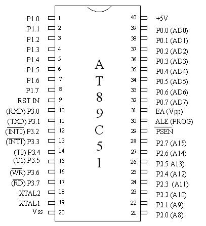
Fig 3.3: – Pin diagram of AT89C51
3.4 Pin Description:
Vcc: Supply voltage.
GND: Ground.
Port 0:
Port 0 is a 8-bit open-deplete bi-directional I/O port. As a yield port, each stick can sink eight TTL inputs. At the point when 1’s are composed to port 0 sticks, the pins can be utilized as high impedance inputs. Port 0 may likewise be arranged to be the multiplexed low request address/information transport amid gets to outside program and information memory. In this mode P0 has inside force ups. Port 0 likewise gets the code bytes amid Flash programming, and yields the code bytes amid program check. Outer force ups are required amid program confirmation.
Port 1:
Port 1 is a 8-bit bi-directional I/O port with inner draw ups. The Port 1 yield cushions can sink/source four TTL inputs. At the point when 1s are composed to Port 1 pins they are pulled high by the inward force ups and can be utilized as data sources. As information sources, Port 1 sticks that are remotely being pulled low will source current (IIL) as a result of the interior force ups. Port 1 additionally gets the low-arrange address bytes amid Flash programming and confirmation.
Port 2:
Port 2 is a 8-bit bi-directional I/O port with inner draw ups. The Port 2 yield supports can sink/source four TTL inputs. At the point when 1s are composed to Port 2 pins they are pulled high by the inner force ups and can be utilized as sources of info. As data sources, Port 2 sticks that are remotely being pulled low will source current (IIL) due to the inner draw ups. Port 2 emanates the high-arrange address byte amid gets from outside program memory and amid gets to outer information memories that use 16-bit addresses (MOVX @DPTR). In this application, it uses strong internal pull-ups when emitting 1s. During accesses to external data memories that use 8-bit addresses (MOVX @ RI), Port 2 emits the contents of the P2 Special Function Register. Port 2 also receives the high-order address bits and some control signals during Flash programming and verification.
Port 3:
Port 3 is a 8-bit bi-directional I/O port with interior force ups. The Port 3 yield supports can sink/source four TTL inputs. At the point when 1s are composed to Port 3 pins they are pulled high by the inward force ups and can be utilized as sources of info. As information sources, Port 3 sticks that are remotely being pulled low will source current (IIL) in view of the draw ups.
Port 3 likewise serves the elements of different unique components of the AT89C51 as recorded beneath:
Port 3 also receives some control signals for Flash programming and verification
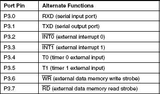
Tab 3.1 Port pins and their alternate functions
RST:
Reset input. A high on this stick for two machine cycles while the oscillator is running resets the gadget.
Brew/PROG:
Address Latch Enable yield beat for hooking the low byte of the deliver amid gets to outside memory. This stick is additionally the program beat input (PROG) amid Flash programming. In ordinary operation ALE is radiated at a consistent rate of 1/6the oscillator recurrence, and might be utilized for outside planning or timing purposes. Note, notwithstanding, that one ALE heartbeat is skipped amid each entrance to outside Data Memory.
On the off chance that coveted, ALE operation can be impaired by setting bit 0 of SFR area 8EH. With the bit set, ALE is dynamic just amid a MOVX or MOVC direction. Something else, the stick isWeakly pulled high. Setting the ALE-incapacitate bit has no impact if the microcontroller is in outside execution mode.
PSEN:
Program Store Enable is the perused strobe to outer program memory. At the point when the AT89C51 is executing code from outside program memory, PSEN is enacted twice each machine cycle, with the exception of that two PSEN actuations are skipped amid each entrance to outer information memory.
EA/VPP:
Outer Access Enable. EA must be strapped to GND keeping in mind the end goal to empower the gadget to get code from outer program memory areas beginning at 0000H up to FFFFH.
Note, in any case, that if bolt bit 1 is customized, EA will be inside hooked on reset.
EA:
EAought to be strapped to VCC for inside program executions. This stick additionally gets the 12-volt programming empower voltage (VPP) amid Flash programming, for parts that require 12-volt VPP.
XTAL1:
Contribution to the reversing oscillator enhancer and contribution to the interior clock working circuit.
XTAL2:
Yield from the reversing oscillator enhancer.
Oscillator Characteristics:
XTAL1 and XTAL2 are the info and yield, individually, of an altering enhancer which can be designed for use as an on-chip oscillator, as appeared in Figs 6.2.3. Either a quartz precious stone or clay resonator might be utilized. To drive the gadget from an outer clock source, XTAL2 ought to be left detached while XTAL1 is driven as appeared in Figure 6.2.4.There are no prerequisites on the obligation cycle of the outside clock motion, since the contribution to the interior timing hardware is through a gap by-two flip-slump, however least and most extreme voltage high and low time determinations must be watched.

.
Fig 3.4 Oscillator Connections Fig 3.4.1 External Clock Drive Configuration
Notes:
1. Under enduring state (non-transient) conditions, IOL must be remotely constrained
as takes after:
• Maximum IOL per port stick: 10 mA
• Maximum IOL per 8-bit port: Port 0: 26 mA
• Ports 1, 2, 3: 15 mA
• Maximum add up to IOL for all yield pins: 71 mA
• If IOL surpasses the test condition, VOL may surpass the related particular. Pins are not ensured to sink current more noteworthy than the recorded test conditions.
2. Minimum VCC for Power-down is 2V.
3.5 REGISTERS:
In the CPU, registers are utilized to store data incidentally. That data could be a byte of information to be prepared, or a deliver indicating the information to be brought. Most by far of 8051 registers are 8–bit registers. In the 8051 there is just a single information sort: 8bits. The 8bits of an enroll are ought to in the outline from the MSB(most noteworthy piece) D7 to the LSB(least critical bit)D0. With a 8-bit information sort, any information bigger than 8bits must be broken into 8-bit pieces before it is prepared. Since there are countless in the 8051, we will focus on a portion of the broadly utilized universally useful registers and cover extraordinary registers in future parts.


D7 D6 D5 D4 D3 D2 D1 D0
The most generally utilized registers of the 8051 are A(accumulator), B, R0, R1, R2, R3, R4, R5, R6, R7, DPTR(data pointer), and PC(program counter). The greater part of the above registers are 8-bits, with the exception of DPTR and the program counter. The collector, enroll An, is utilized for all number juggling and rationale guidelines.
SFRs (Special Function Registers)
Among the registers R0-R7 are a piece of the 128 bytes of RAM memory
shouldn’t something be said about registers A,B, PSW, and DPTR? Do they likewise have addresses? The appropriate response is yes. In the 8051, registers A, B, PSW and DPTR are a piece of the gathering of registers regularly alluded to as SFR (exceptional capacity registers). There are numerous unique capacity registers and they are generally utilized. The SFR can be gotten to by the names (which is substantially less demanding) or by their locations. For instance, enroll A has address E0h, and enlist B has been touched off the address F0H, as appeared in table.
The accompanying two focuses ought to noted about the SFR addresses.
1. The Special capacity registers have addresses in the vicinity of 80H and FFH. These locations are over 80H, since the locations 00 to 7FH are locations of RAM memory inside the 8051.
2. Not all the deliver space of 80H to FFH is utilized by the SFR. The unused areas 80H to FFH are held and should not be utilized by the 8051 software engineer.
As to tending to mode, see the accompanying two focuses: (a) the
deliver esteem is restricted to one byte, 00-FFH, which implies this tending to mode is limited to accessing RAM locations and registers located inside the 8051. (b) if you examine the lst file for an assembly language program, you will see that the SFR registers names are replaced with their addresses as listed in table.
| Symbol | Name | Address |
| ACC | Accumulator | 0E0H |
| B | B register | 0F0H |
| PSW | Program status word | 0D0H |
| SP | Stack pointer | 81H |
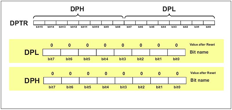
| DPTR | Data pointer 2 bytes | |
| DPL | Low byte | 82H |
| DPH | High byte | 83H |
| P0 | Port0 | 80H |
| P1 | Port1 | 90H |
| P2 | Port2 | 0A0H |
| P3 | Port3 | 0B0H |
| IP | Interrupt priority control | 0B8H |
| IE | Interrupt enable control | 0A8H |
| TMOD | Timer/counter mode control | 89H |
| TCON | Timer/counter control | 88H |
| T2CON | Timer/counter 2 control | 0C8H |
| T2MOD | Timer/counter mode2 control | 0C9H |
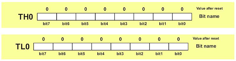
| TH0 | Timer/counter 0high byte | 8CH |
| TL0 | Timer/counter 0 low byte | 8AH |
| TH1 | Timer/counter 1 high byte | 8DH |
28
| TL1 | Timer/counter 1 low byte | 8BH |
| TH2 | Timer/counter 2 high byte | 0CDH |
| TL2 | Timer/counter 2 low byte | 0CCH |
| RCAP2H | T/C 2 capture register high byte | 0CBH |
| RCAP2L | T/C 2 capture register low byte | 0CAH |
| SCON | Serial control | 98H |
| SBUF | Serial data buffer | 99H |
| PCON | Power control | 87H |
Tab 3.2: 8051 Special function register Address
ARegister(Accumulator)

This is a broadly useful enlist which serves for putting away middle outcomes amid working. A number (an operand) ought to be added to the aggregator before execute a direction upon it. Once an arithmetical operation is preformed by the ALU, the outcome is put into the collector. On the off chance that an information ought to be exchanged starting with one enlist then onto the next, it must experience aggregator. For such all inclusive reason, this is the most usually utilized enlist that none microcontroller can be envisioned without (more than a half 8051 microcontroller’s directions utilized utilize the gatherer somehow).
B Register
B enlist is utilized amid duplicate and partition operations which can be performed just upon numbers put away in the An and B registers. Every single other direction in the program can utilize this enlist as an extra gatherer (A).

Note: Amid programming, each of registers is called by name so that their correct address is not all that essential for the client. Amid gathering into machine code (arrangement of hexadecimal numbers perceived as guidelines by the microcontroller), PC will consequently, rather than registers’ name, compose fundamental locations into the microcontroller.
R Registers (R0-R7)
his is a common name for the total 8 generalpurpose registers (R0, R1, R2…R7). Even they are not true SFRs, they deserve to be discussed here because of their motivation. The bank is dynamic when the R registers it incorporates are being used. Like the aggregator, they are utilized for brief putting away factors and halfway outcomes. Which of the banks will be dynamic relies on upon two bits incorporated into the PSW Register. These registers are put away in four banks in the extent of RAM.
The accompanying case best outlines the valuable reason for these registers. Assume that scientific operations on numbers beforehand put away in the R registers ought to be performed: (R1+R2) – (R3+R4). Clearly, an enlist for impermanent putting away consequences of expansion is required. Everything is very basic and the program is as per the following :
MOV A,R3; Means: move number from R3 into gatherer
Include A,R4; Means: add number from R4 to gatherer (result stays in
gatherer)
MOV R5,A; Means: incidentally move the outcome from gatherer into R5
MOV A,R1; Means: move number from R1 into collector
Include A,R2; Means: add number from R2 to collector
SUBB A,R5; Means: subtract number from R5 ( there are R3+R4 )
8051 Register Banks and Stack
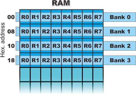
Slam memory space assignment in the 8051
There are 128 bytes of RAM in the 8051. The 128 bytes of RAM inside the 8051 are relegated addresses 00 to7FH. These 128 bytes are isolated into three unique gatherings as takes after:
1. A aggregate of 32 bytes from areas 00 to 1FH hex are put aside for enlist banks and the stack.A aggregate of 16 bytes from areas 20 to 2FH hex are put aside for bit-addressable read/compose memory.
2. A aggregate of 80 bytes from areas 30H to 7FH are utilized for perused and compose stockpiling, or what is ordinarily called Scratch cushion. These 80 areas of RAM are generally utilized with the end goal of putting away information and parameters nu 8051 software engineers.
Enlist banks in the 8051
A sum of 32bytes of RAM are put aside for the enlist banks and stack. These 32 bytes are separated into 4 banks of registers in which each bank has registers, R0-R7. smash areas 0 to 7 are put aside for bank 0 of R0-R7 where R0is RAM area 0, R1 is RAM area 1, R2 is area 2, et cetera, until memory location7, which has a place with R7 of bank0. the second bank of registers R0-R7 begins at RAM area 08 and goes to area 0FH. The third bank of R0-R7 begins at memory area 10H and goes to area 17H. At last, RAM areas 18H to 1FH are put aside for the fourth bank of R0-R7. fig demonstrates how the 32 bytes are assigned into 4 banks.
As should be obvious from fig 1, the bank 1 utilizes a similar RAM space as the stack. This is a noteworthy issue in programming the 8051. we should either not utilize enroll bank1, or apportion another territory of RAM for the stack.
Default enroll bank
In case RAM territories 00-1F are set aside for the four select banks, which enroll bank of R0-R7 do we have permission to when the 8051 is controlled up? The proper reaction is enroll bank 0; that is , RAM territories 0, 1,2,3,4,5,6, and 7 are gotten to with the names R0, R1, R2, R3, R4, R5, R6, and R7 when programming the 8051. It is considerably less difficult to insinuate these RAM ranges with
Default register bank
On the off chance that RAM areas 00-1F are put aside for the four enroll banks, which enlist bank of R0-R7 do we have entry to when the 8051 is controlled up? The appropriate response is enlist bank 0; that is , RAM areas 0, 1,2,3,4,5,6, and 7 are gotten to with the names R0, R1, R2, R3, R4, R5, R6, and R7 when programming the 8051. It is significantly simpler to allude to these RAM areas with names such as R0, R1 and so on, than by their memory locations as shown in fig 2.The register banks are switched by using the D3 & D4 bits of register PSW.
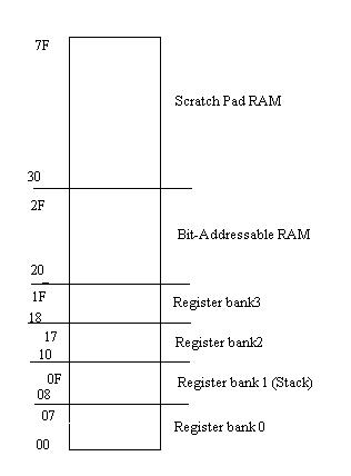
Fig :3.5 RAM Allocation in the 8051
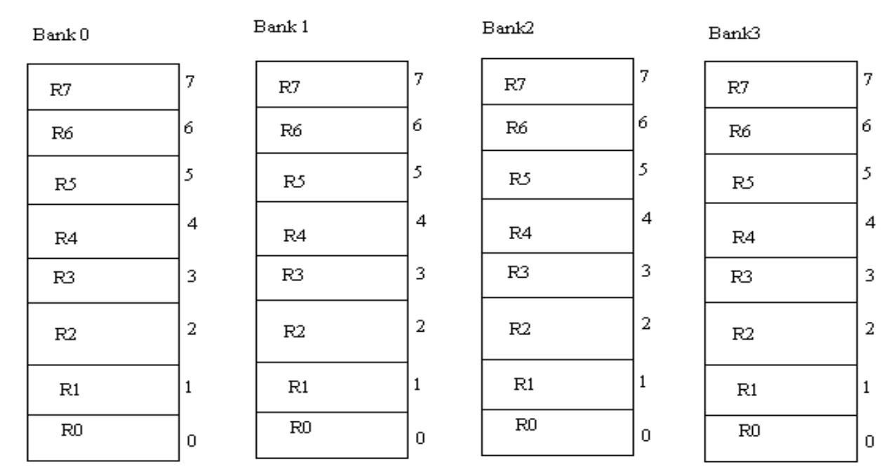
Fig: 3.5.1 8051 Register Banks and their RAM Addresses
PSW Register (Program Status Word)

This is a standout amongst the most imperative SFRs. The Program Status Word (PSW) contains a few status bits that mirror the present condition of the CPU. This enroll contains: Carry bit, Auxiliary Carry, two enlist bank select bits, Overflow signal, equality bit, and client quantifiable status hail. The ALU naturally changes some of enlist’s bits, which is generally utilized as a part of direction of the program performing.
P – Parity bit. On the off chance that a number in aggregator is and still, at the end of the day this bit will be consequently set (1), else it will be cleared (0). It is basically utilized amid information transmission and accepting through serial correspondence.
– Bit 1. This bit is expected for the future variants of the microcontrollers, so it shouldn’t be here.
OV Overflow happens when the aftereffect of arithmetical operation is more prominent than 255 (deci mal), with the goal that it can not be put away in one enroll. All things considered, this bit will be set (1). In the event that there is no flood, this bit will be cleared (0).
RS0, RS1 –
Register bank select bits. These two bits are utilized to choose one of the four enlist banks in RAM. By composing ones to these bits, a gathering of registers R0-R7 is put away in one of four banks in RAM.
| RS1 | RS2 | Space | in | ||


| RAM | ||||||
| 0 | 0 | Bank0 | 00h- | |||
| 07h | ||||||
| 0 | 1 | Bank1 | 08h- | |||
| 0Fh | ||||||
| 1 | 0 | Bank2 | 10h- | |||
| 17h | ||||||
| 1 | 1 | Bank3 | 18h- | |||
| 1Fh | ||||||
Tab 3.3:Register banks selection bits
F0 – Flag 0. This is a broadly useful piece accessible to the client.
Auxiliary Carry Flag is utilized for BCD operations as it were.
CY – Carry Flag is the (ninth) assistant piece utilized for every single arithmetical operation what’s more, move guidelines.
DPTR Register (Data Pointer)
These registers are not genuine ones since they don’t physically exist. They comprise of two separate registers: DPH (Data Pointer High) and (Data Pointer Low). Their 16 bits are utilized for outside memory tending to. They might be taken care of as a 16-bit enlist or as two free 8-bit registers. In addition, the DPTR Register is generally utilized for putting away information and middle of the road comes about which have nothing to do with memory areas.
SP REGISTER( Stack Pointer)

The stack is a segment of RAM utilized by the CPU to store data temporily. This data could be information or an address. The CPU needs this stockpiling zone since there are just a predetermined number of registers.
How stacks are gotten to in the 8051. In the event that the stack is an area of RAM, there must be registers inside the CPU to indicate it. The enlist used to get to the stack is known as the SP (Stack point) Register. The stack pointer in the 8051 is just 8 bits wide, which implies that it can take estimations of 00 to FFH. At the point when the 8051 is fueled up, the SP enlist contains esteem 07. This implies RAM area 08 is the principal area utilized for the stack by the 8051. The putting away of a CPU enroll in the stack is known as a PUSH, and pulling the substance off the stack over into a CPU enlist is known as a POP. As it were, an enlist is pushed onto the stack to spare it and flown off the stack to recover it. The employment of the SP is extremely basic when push and pop activities are performed.
Pushing onto the stack:
In the 8051 the stack pointer (SP) focuses to the last utilized area of the stack. As we push information onto the stack, the stack pointer is augmented by one. See that this unique in relation to numerous miniaturized scale processors, eminently x86 processors in which the SP is decremented when information is pushed onto the stack. As each PUSH is executed, the substance of the enlist are saved money on the stack and SP is augmented by 1. See that for each byte of information saved money on the stack, SP is augmented just once. See likewise that to push the registers onto the stack we should utilize their RAM addresses. For instance, the direction ― PUSH‖ pushes enlist R1 onto the stack.
Flying from the stack:
Popping the substance of the stack again into a given enroll is the inverse procedure of pushing. With each pop, the top byte of the stack is replicated to the enroll indicated by the guideline and the stack pointer is decremented once.
The maximum furthest reaches of the stack As, said prior, areas 08 to 1FH in the 8051 RAM can be utilized for the stack. This is on account of areas 20-2FH of RAM are held for bit-addressable memory and must not be utilized by the stack. In the event that in a program we require more than 24 bytes (08 to 1FH=24bytes) of stack, we can change the SP to indicate RAM areas 30-7FH. This is finished with the guideline ―MOV SP, #XX‖.

The maximum furthest reaches of the stack
As, said prior, areas 08 to 1FH in the 8051 RAM can be utilized for the stack. This is on account of areas 20-2FH of RAM are held for bit-addressable memory and must not be utilized by the stack. In the event that in a program we require more than 24 bytes (08 to 1FH=24bytes) of stack, we can change the SP to indicate RAM areas 30-7FH. This is finished with the guideline ―MOV SP, #XX‖.
P0, P1, P2, P3 – Input/Output Registers
In the event that that outside memory and serial correspondence framework are not being used then, 4 ports with altogether of 32 info yield lines are accessible to the client for association with fringe condition. Each piece inside these ports compares to the suitable stick on the microcontroller. This implies rationale state kept in touch with these ports shows up as a voltage on the stick ( 0 or 5 V). Actually, while perusing, the inverse happens – voltage on some information pins is reflected in the fitting port piece.
The condition of a port piece, other than being reflected in the stick, decides in the meantime whether it will be arranged as info or yield. In the event that a bit is cleared (0), the stick will be arranged as yield. In a similar way, if a bit is set to 1 the stick will be arranged as information. After reset, and when turning the microcontroller on , all bits on these ports are set to one (1). This implies the proper pins will be arranged as sources of info.
Program counter:
The essential enroll in the 8051 is the PC (Program counter). The program counter indicates the address of the following direction to be executed. As the CPU gets the opcode from the program ROM, the program counter is augmented to indicate the following direction. The program counter in the 8051 is 16bits wide. This implies the 8051 can get to program addresses 0000 to FFFFH, an aggregate of 64k bytes of code. Be that as it may, not all individuals from the 8051 have the whole 64K bytes of on-chip ROM introduced, as we will see soon.
3.6 Types of directions:
Contingent upon operation they play out, all directions are partitioned in a few gatherings:
• Arithmetic Instructions
• Branch Instructions
• Data Transfer Instructions
• Logical Instructions
• Logical Instructions with bits
The initial segment of every direction, called MNEMONIC alludes to the operation a guideline performs (replicating, expansion, sensible operation and so forth.). Memory helpers usually are abbreviated type of name of operation being executed. For instance:
INCR1; IncrementR1(incrementregisterR1)
LJMP LAB5 ; Long Jump LAB5 (long bounce to address indicated as LAB5)
JNZ LOOP ; Jump if Not Zero LOOP (if the number in the gatherer
is not 0, hop to address indicated as LOOP)
Another piece of direction, called OPERAND is isolated from memory helper at any rate by one exhaust space and characterizes information being handled by guidelines. A few directions have no operand; some have one, a few. On the off chance that there is more than one operand in guideline, they are isolated by comma. For instance:
RET – (return from sub-schedule)
JZ TEMP – (if the number in the gatherer is not 0, bounce to address indicated
as TEMP)
ADD A,R3 – (add R3 and accumulator)
CJNE A,#20,LOOP – (contrast collector and 20. On the off chance that they are not equivalent, bounce
to address specified as LOOP)
Number-crunching directions
These directions play out a few essential operations ( expansion, subtraction, division, duplication and so on.) After execution, the outcome is put away in the principal operand. For instance:
Include A, R1 – The aftereffect of expansion (A+R1) will be put away in the aggregator.
Branch Instructions
There are two sorts of these directions:
Unlimited hop guidelines: After their execution a bounce to another area from where the program proceeds with execution is executed.
Contingent hop guidelines: If some condition is met – a hop is executed. Something else, the program typically continues with the following guideline.
Information Transfer Instructions:
These directions move the substance of one enroll to another. The enroll which substance is moved stays unaltered. On the off chance that they have the addition ―X‖
(MOVX), the information is traded with outside memory.
Consistent Instructions
These directions perform coherent operations between comparing bits of two registers. After execution, the outcome is put away in the main operand.
Legitimate Operations on Bits
Like sensible directions, these guidelines perform coherent operations. The distinction is that these operations are performed on single bits.
3.7 TIMERS:
On-chip timing/tallying office has demonstrated the capacities of the microcontroller for actualizing the constant application. These incorporates beat numbering, recurrence estimation, beat width estimation, baud rate era, and so on,. Having adequate number of clock/counters might be a need in a specific plan application. The 8051 has two clocks/counters. They can be utilized either as clocks to create a period delay or as counters to tally occasions occurring outside the microcontroller. Let examine how these clocks are utilized to create time postponements and we will likewise talk about how they are been utilized as occasion counters.
PROGRAMMING 8051 TIMERS
The 8051 has clocks: Timer 0 and Timer1.they can be utilized either as clocks or as occasion counters. Give us initial a chance to talk about the clocks’ registers and how to program the clocks to create time delays.
Fundamental Registers of the Timer
Both Timer 0 and Timer 1 are 16 bits wide. Since the 8051 has a 8-bit engineering, every 16-bit clock is gotten to as two separate registers of low byte and high byte.
Clock 0 REGISTERS
The 16-bit enlist of Timer 0 is gotten to as low byte and high byte. the low byte enlist is called TL0(Timer 0 low byte)and the high byte enroll is alluded to as TH0(Timer 0 high byte).These enlist can be gotten to like whatever other enlist, for example, A,B,R0,R1,R2,etc.for illustration, the direction
‖MOV TL0, #4F‖moves the esteem 4FH into TL0,the low byte of Timer 0.These registers can likewise be perused like whatever other enlist.
Clock 1 REGISTERS
Clock 1 is likewise 16-bit enroll is part into two bytes, alluded to as TL1 (Timer 1 low byte) and TH1(Timer 1 high byte).these registers are available n an indistinguishable route from the enlist of Timer 0.
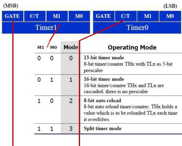
TMOD (clock mode) REGISTER
Both clocks 0 and 1 utilize a similar enlist, called TMOD, to set the different clock operation modes. TMOD is a 8-bit enroll in which the lower 4 bits are put aside for Timer 0 and the upper 4 bits for Timer 1.in each case; the lower 2 bits are utilized to set the clock mode and the upper 2 bits to determine the operation.
MODES: M1, M0:
M0 and M1 are utilized to choose the clock mode. There are three modes: 0, 1, 2.Mode 0 is a 13-bit clock, mode 1 is a 16-bit clock, and mode 2 is a 8-bit clock. We will focus on modes 1 and 2 since they are the ones utilized generally broadly. we will soon portray the attributes of these modes, in the wake of depicting the reset of the TMOD enlist.
Entryway
Entryway control when set. The clock is empowered just while the INTx stick is high and the TRx control stick is set. Whenever cleared, the clock is enabled.C/T
Clock or counter chose cleared for clock operation (Input from inside framework clock).set for counter Operation (input TX input stick).
C/T (clock/clock):
This bit in the TMOD enroll is utilized to choose whether the clock is utilized as a defer generator or an occasion counter. In the event that C/T=0, it is utilized as a clock for time postpone era. The clock hotspot for the time postponement is the gem recurrence of the 8051.this area is worried with this decision. The clock’s utilization as an occasion counter is talked about in the following segment.
Serial Communication:
PCs can move information in two ways: parallel and serial. In parallel information exchanges, frequently at least 8 lines (wire transmitters) are utilized to exchange information to a gadget that is just a couple of feet away. Cases of parallel transfersae printers and hard plates; each utilizations links with many wire strips. In spite of the fact that in such cases a considerable measure of information can be moved in a short measure of time by utilizing many wires in parallel, the separation can’t be awesome. To exchange to a gadget found numerous
meters away, the serial technique is utilized. In serial correspondence, the information is sent one piece at once, rather than parallel correspondence, in which the information is sent a byte or more at any given moment. Serial correspondence of the 8051 is the point of this part. The 8051 has serial correspondence ability incorporated with it, there by making conceivable quick information exchange utilizing just a couple wires.
On the off chance that information is to be exchanged on the phone line, it must be changed over from 1s to sound tones, which are sinusoidal-formed signs. A fringe gadget called a modem, which remains for ―modulator/demodulator‖, plays out this transformation.
Serial information correspondence utilizes two techniques, nonconcurrent and synchronous. The synchronous technique exchanges a square of information at any given moment, while the nonconcurrent strategy exchanges a solitary byte at any given moment.
In information transmission if the information can be transmitted and gotten, it is a duplex transmission. This is as opposed to simplex transmissions, for example, with printers, in which the PC just sends information. Duplex transmissions can be half or full duplex, contingent upon regardless of whether the information exchange can be concurrent. In the event that information is transmitted one route at once, it is alluded to as half duplex. On the off chance that the information can go both courses in the meantime, it is full duplex. Obviously, full duplex requires two wire conduits for the information lines, one for transmission and one for gathering, keeping in mind the end goal to exchange and get information all the while.
Nonconcurrent serial correspondence and information surrounding
The information coming in at the less than desirable end of the information line in a serial information exchange is each of the 1s; it is hard to comprehend the information unless the sender and recipient concur on an arrangement of guidelines, a convention, on how the dat
Program counter:
The important register in the 8051 is the PC (Program counter). The program counter points to the address of the next instruction to be executed. As the CPU fetches the opcode from the program ROM, the program counter is incremented to point to the next instruction. The program counter in the 8051 is 16bits wide. This means that the 8051 can access program addresses 0000 to FFFFH, a total of 64k bytes of code. However, not all members of the 8051 have the entire 64K bytes of on-chip ROM installed, as we will see soon.
3.6 Types of instructions:
Depending on operation they perform, all instructions are divided in several groups:
- Arithmetic Instructions
- Branch Instructions
- Data Transfer Instructions
- Logical Instructions
- Logical Instructions with bits
The first part of each instruction, called MNEMONIC refers to the operation an instruction performs (copying, addition, logical operation etc.). Mnemonics commonly are shortened form of name of operation being executed. For example:
| INCR1; | IncrementR1(incrementregisterR1) |
| LJMP LAB5 ; | Long Jump LAB5 (long jump to address specified as LAB5) |
JNZ LOOP ; Jump if Not Zero LOOP (if the number in the accumulator
is not 0, jump to address specified as LOOP)
Another part of instruction, called OPERAND is separated from mnemonic at least by one empty space and defines data being processed by instructions. Some instructions have no operand; some have one, two or three. If there is more than one operand in instruction, they are separated by comma. For example:
RET – (return from sub-routine)
JZ TEMP – (if the number in the accumulator is not 0, jump to address specified
| as | TEMP) | |||||
| ADD | A,R3 | – | (add | R3 | and | accumulator) |
CJNE A,#20,LOOP – (compare accumulator with 20. If they are not equal, jump to address specified as LOOP)
Arithmetic instructions

 Arithmetical Instructions
| Mnemonic | Description | Byte | Oscillator |
| Number | Period | ||
| ADD A,Rn | Add R Register to accumulator | 1 | 1 |
| ADD A,Rx | Add directly addressed Rx Register to | 2 | 2 |
| accumulator | |||
| ADD | Add indirectly addressed Register to | 1 | 1 |


| A,@Ri | accumulator | |||
| ADD A,#X | Add number X to accumulator | 2 | 2 | |
| ADDC | Add R Register with Carry bit | to | 1 | 1 |
| A,Rn | accumulator | |||


Branch Instruction
| Mnemonic | Description | Byte | Oscillator | |
| Number | Period | |||
| ACALL | Call subroutine located at address within 2 | 2 | 3 | |
41
| adr11 | K byte Program Memory space | |||
| LCALL | Call subroutine located at any | address | 3 | 4 |
| adr16 | within 64 K byte Program Memory space | |||
| RET | Return from subroutine | 1 | 4 | |
| RETI | Return from interrupt routine | 1 | 4 | |
| AJMP | Jump to address located within 2 K byte | 2 | 3 | |
| adr11 | Program Memory space | |||
| LJMP | Jump to any address located within 64 K | 3 | 4 | |
| adr16 | byte Program Memory space | |||


Data Transfer Instruction
| Mnemonic | Description | Byte | Cycle | |
| Number | Number | |||
| MOV | Move R register to accumulator | 1 | 1 | |
| A,Rn | ||||
| MOV | Move directly addressed Rx register to | 2 | 2 | |
| A,Rx | accumulator | |||
| MOV | Move indirectly addressed register to | 1 | 1 | |
| A,@Ri | accumulator | ||
| MOV | Move number X to accumulator | 2 | 2 |
| A,#X | |||
Logical Instructions
These instructions perform logical operations between corresponding bits of two registers. After execution, the result is stored in the first operand.

Logical Instructions
| Mnemonic | Description | Byte | Cycle |
| Number | Number | ||
| ANL A,Rn | Logical AND between accumulator and R | 1 | 1 |
| register | |||
| ANL A,Rx | Logical AND between accumulator and | 2 | 2 |
| directly addressed register Rx | |||
| ANL | Logical AND between accumulator and | 1 | 1 |
| A,@Ri | indirectly addressed register | ||
| ANL A,#X | Logical AND between accumulator and | 2 | 2 |
| number X | |||


Logical Operations on Bits
Similar to logical instructions, these instructions perform logical operations. The difference is that these operations are performed on single bits.

Logical operations on bits
| Mnemonic | Description | Byte | Cycle |
| Number | Number | ||
| CLR C | Clear Carry bit | 1 | 1 |
| CLR bit | Clear directly addressed bit | 2 | 2 |
| SETB C | Set Carry bit | 1 | 1 |
| SETB bit | Set directly addressed bit | 2 | 2 |
| CPL C | Complement Carry bit | 1 | 1 |
| CPL bit | Complement directly addressed bit | 2 | 2 |

RS232 pins
RS232 cable, commonly referred to as the DB-25 connector. In labeling, DB-25P refers to the plug connector (male) and DB-25S is for the socket connector(female). Since not all the pins are used in PC cables, IBM introduced the DB-9 Version of the serial I/O standard, which uses 9 pins only, as shown in
table.
DB-9 pin connector

1 2 3 4 5
6 7 8 9

(Out of computer and exposed end of cable)
| Pin | Description |
| 1 | Data carrier detect (DCD) |
| 2 | Received data (RXD) |
| 3 | Transmitted data (TXD) |
| 4 | Data terminal ready(DTR) |
| 5 | Signal ground (GND) |
| 6 | Data set ready (DSR) |
| 7 | Request to send (RTS) |
| 8 | Clear to send (CTS) |
| 9 | Ring indicator (RI) |
Tab:3.4 Pin functions of RS232 Note: DCD, DSR, RTS and CTS are active low pins.
The method used by RS-232 for communication allows for a simple connection of three lines: Tx, Rx, and Ground. The three essential signals for 2-way RS-232 Communications are these:
TXD: carries data from DTE to the DCE. RXD: carries data from DCE to the DTE SG: signal ground
8051 connection to RS232:
RS232 link, generally alluded to as the DB-25 connector. In marking, DB-25P alludes to the attachment connector (male) and DB-25S is for the attachment connector(female). Since not every one of the pins are utilized as a part of PC links, IBM presented the DB-9 Version of the serial I/O standard, which utilizes 9 sticks just, as appeared in
The 8051 has two sticks that are utilized particularly to transfer and getting information serially. These two pins are called TXD and RXD and a piece of the port 3 gathering (P3.0 and P3.1). Stick 11 of the 8051 is doled out to TXD and stick 10 is assigned as RXD. These pins are TTL perfect; in this manner, they require a line driver to make them RS232 good. One such line driver is the MAX232 chip.
MAX232 changes over from RS232 voltage levels to TTL voltage levels, and the other way around. One favorable position of the MAX232 chip is that it utilizes a +5V control source which, is the same as the source voltage for the 8051. In alternate words, with a solitary +5V control supply we can control both the 8051 and MAX232, with no requirement for the power supplies that are normal in numerous more seasoned frameworks. The MAX232 has two arrangements of line drivers for exchanging and getting information. The line drivers utilized for TXD are called T1 and T2, while the line drivers for RXD are assigned as R1 and R2. In numerous applications just a single of each is utilized.
CHAPTER-4
4.1 Introduction
The power supplies are intended to change over high voltage AC mains power to a reasonable low voltage supply for gadgets circuits and different gadgets. A power supply can by separated into a progression of obstructs, each of which plays out a specific capacity. A d.c control supply which keeps up the yield voltage consistent regardless of a.c mains changes or load varieties is known as
For instance a 5V managed control supply framework as demonstrated as follows:
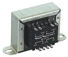
4.2 TRANSFORMER
A transformer is an electrical gadget which is utilized to change over electrical power starting with one Electrical circuit then onto the next without change in recurrence.
Transformers change over AC power starting with one voltage then onto the next with little loss of energy. Transformers work just with AC and this is one reason why mains power is AC. Venture up transformers increment in yield voltage, venture down transformers diminish in yield voltage. Most power supplies utilize a stage down transformer to diminish the hazardously high mains voltage to a more secure low voltage. The information loop is known as the essential and the yield curl is known as the optional. There is no electrical association between the two curls; rather they are connected by an exchanging attractive field made in the delicate iron center of the transformer. The two lines amidst the circuit image speak to the center. Transformers squander next to no power so the power out is (practically) equivalent to the power in. Take note of that as voltage is ventured down current is ventured up. The proportion of the quantity of turns on each loop, called the turn’s proportion, decides the proportion of the voltages. A stage down transformer has a substantial number of turns on its essential (info) curl which is associated with the high voltage mains supply, and few turns on its optional (yield) loop to give a low yield voltage.
4.2 An Electrical Transformer
Turns proportion = VP/VS = NP/NS
Control Out= Power In
Versus X IS=VP X IP
VP= essential (info) voltage
NP=number of turns on essential curl
IP= essential (info) current
4.3 RECTIFIER:
A circuit which is utilized to change over a.c to dc is known as RECTIFIER. The procedure of transformation a.c to d.c is called ―rectification‖
Sorts OF RECTIFIERS:
• Half wave Rectifier
• Full wave rectifier
1. Centre tap full wave rectifier.
2. Bridge sort full extension rectifier.
Connect Rectifier: An extension rectifier makes utilization of four diodes in a scaffold course of action to accomplish full-wave amendment. This is a broadly utilized setup, both with individual diodes wired as appeared and with single segment extensions where the diode scaffold is wired inside.
A scaffold rectifier makes utilization of four diodes in an extension plan as appeared in fig(a) to accomplish full-wave amendment. This is a generally utilized setup, both with individual diodes wired as appeared and with single segment extensions where the diode scaffold is wired inside.
4.4 FILTER
A Filter is a gadget which evacuates the a.c part of rectifier yield however permits the d.c segment to achieve the heap
Capacitor Filter:
We have seen that the swell substance in the corrected yield of half wave rectifier is 121% or that of full-wave or scaffold rectifier or extension rectifier is 48% such high rates of swells is not adequate for the vast majority of the applications. Swells can be evacuated by one of the accompanying techniques for sifting.
(a) A capacitor, in parallel to the heap, gives a simpler by –pass to the swells voltage however it because of low impedance. At swell recurrence and leave the d.c.to shows up the heap.
(b) An inductor, in arrangement with the heap, keeps the section of the swell current (because of high impedance at swell recurrence) while permitting the d.c (because of low imperviousness to d.c)
(c) different mixes of capacitor and inductor, for example, L-segment channel area channel, numerous segment channel and so forth which make utilization of both the properties specified in (an) and (b) above. Two instances of capacitor channel, one connected on half wave rectifier and another with full wave rectifier.
Separating is performed by an expansive esteem electrolytic capacitor associated over the DC supply to go about as a store, providing current to the yield when the changing DC voltage from the rectifier is falling. The capacitor charges rapidly close to the pinnacle of the changing DC, and afterward releases as it supplies current to the yield. Sifting altogether builds the normal DC voltage to nearly the pinnacle esteem (1.4 × RMS esteem).
To compute the estimation of capacitor(C), C = ¼*√3*f*r*Rl
Where,
f = supply recurrence, r = swell component,
Rl = stack resistance
Note: In our circuit we are utilizing 1000µF Hence vast estimation of capacitor is put to lessen swells and to enhance the DC part.
4.5 REGULATOR
Voltage controller ICs is accessible with settled (regularly 5, 12 and 15V) or variable yield voltages. The most extreme current they can pass likewise rates them. Negative voltage controllers are accessible, principally for use in double supplies. Most controllers incorporate some programmed insurance from exorbitant current (‘over-burden assurance’) and overheating (‘warm security’). A significant number of the settled voltage controller ICs have 3 leads and look like power transistors, for example, the 7805 +5V
1A controller appeared on the privilege. The LM7805 is easy to utilize. You essentially interface the positive lead of your unregulated DC control supply (anything from 9VDC to 24VDC) to the Input stick, associate the negative prompt the Common stick and after that when you turn on the power, you get a 5 volt supply from the yield stick.
Fig:4.1 Block diagram of Power supply
53
54
55
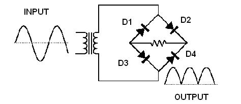
Fig:4.3 Bridge Rectifier circuit
Operation:
During positive half cycle of secondary, the diodes D2 and D3 are in forward biased while D1 and D4 are in reverse biased as shown in the fig(b). The current flow direction is shown in the fig (b) with dotted arrows.
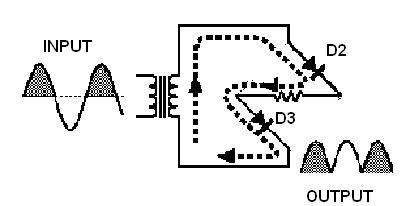
Fig:4.3.1 Operation under positive cycle
0
During negative half cycle of secondary voltage, the diodes D1 and D4 are in forward biased while D2 and D3 are in reverse biased as shown in the fig(c). The current flow direction is shown in the fig (c) with dotted arrows.
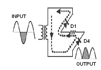
Fig:4.3.2 Operation under negative cycle
4.4 FILTER
A Filter is a device which removes the a.c component of rectifier output but allows the d.c component to reach the load
Capacitor Filter:
We have seen that the ripple content in the rectified output of half wave rectifier is 121% or that of full-wave or bridge rectifier or bridge rectifier is 48% such high percentages of ripples is not acceptable for most of the applications. Ripples can be removed by one of the following methods of filtering.
- A capacitor, in parallel to the load, provides an easier by –pass for the ripples voltage though it due to low impedance. At ripple frequency and leave the d.c.to appears the load.
- An inductor, in series with the load, prevents the passage of the ripple current (due to high impedance at ripple frequency) while allowing the d.c (due to low resistance to d.c)
(c) various combinations of capacitor and inductor, such as L-section filter  section filter, multiple section filter etc. which make use of both the properties mentioned in (a) and (b) above. Two cases of capacitor filter, one applied on half wave rectifier and another with full wave rectifier.
Filtering is performed by a large value electrolytic capacitor connected across the DC supply to act as a reservoir, supplying current to the output when the varying DC voltage from the rectifier is falling. The capacitor charges quickly near the peak of the varying DC, and then discharges as it supplies current to the output. Filtering significantly increases the average DC voltage to almost the peak value (1.4 × RMS value).
To calculate the value of capacitor(C), C = ¼*√3*f*r*Rl
Where,
f = supply frequency, r = ripple factor,
Rl = load resistance
Note: In our circuit we are using 1000µF Hence large value of capacitor isplaced to reduce ripples and to improve the DC component.
4.5 REGULATOR
Voltage regulator ICs is available with fixed (typically 5, 12 and 15V) or variable output voltages. The maximum current they can pass also rates them. Negative voltage regulators are available, mainly for use in dual supplies. Most regulators include some automatic protection from excessive current (‘overload protection’) and overheating (‘thermal protection’). Many of the fixed voltage regulator ICs have 3 leads and look like power transistors, such as the 7805 +5V
1A regulator shown on the right. The LM7805 is simple to use. You simply connect the positive lead of your unregulated DC power supply (anything from 9VDC to 24VDC) to the Input pin, connect the negative lead to the Common pin and then when you turn on the power, you get a 5 volt supply from the output pin.
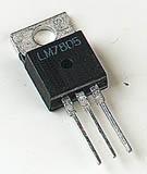
Fig 4.4 Three Terminal Voltage Regulator
Features:
- Output Current of 1.5A
- Output Voltage Tolerance of 5%
- Internal thermal overload protection
- Internal Short-Circuit Limited
- No External Component
- Output Voltage 5.0V, 6V, 8V, 9V, 10V,12V, 15V, 18V, 24V
- Offer in plastic TO-252, TO-220 & TO-263
- Direct Replacement for LM78XX
CHAPTER-5
Description of Liquid Crystal Display
Fluid precious stone presentations (LCDs) have materials, which consolidate the properties of both fluids and gems. As opposed to having a softening point, they have a temperature run inside which the atoms are nearly as portable as they would be in a fluid, yet are gathered together in a requested frame like a precious stone.
A LCD comprises of two glass boards, with the fluid gem material sand witched in the middle of them. The inward surface of the glass plates are covered with straightforward terminals which characterize the character, images or examples to be shown polymeric layers are available in the middle of the anodes and the fluid precious stone, which makes the fluid gem particles to keep up a characterized introduction point.
One every polarisers are glued outside the two glass boards. These polarisers would turn the light beams going through them to a clear edge, in a specific heading.
At the point when the LCD is in the off state, light beams are pivoted by the two polarisers and the fluid precious stone, to such an extent that the light beams left the LCD with no introduction, and subsequently the LCD seems straightforward.
At the point when adequate voltage is connected to the terminals, the fluid gem atoms would be adjusted in a particular heading. The light beams going through the LCD would be turned by the polarisers, which would bring about initiating/highlighting the coveted characters.
The LCD’s are lightweight with just a couple of millimeters thickness. Since the LCD’s expend less power, they are perfect with low power electronic circuits, and can be controlled for long lengths.
The LCD’s don’t produce light thus light is expected to peruse the show. By utilizing backdrop illumination, perusing is conceivable oblivious. The LCD’s have long life and a wide working temperature go.
Changing the show estimate or the design size is moderately straightforward which makes the LCD’s more clients agreeable.
The LCDs utilized only in watches, adding machines and measuring instruments are the straightforward seven-fragment shows, having a restricted measure of numeric information. The current advances in innovation have brought about better clarity, more data showing capacity and a more extensive temperature run. These have brought about the LCDs being widely utilized as a part of broadcast communications and excitement hardware. The LCDs have even begun supplanting the cathode beam tubes (CRTs) utilized for the show of content and design, and furthermore in little TV applications.
This area portrays the operation methods of LCD’s then depict how to program and interface a LCD to 8051 utilizing Assembly and C.
5.1 LCD operation
As of late the LCD is finding across the board utilize supplanting LEDs (seven-fragment LEDs or other multi section LEDs).This is because of the accompanying reasons:
1. The declining costs of LCDs.
2. The capacity to show numbers, characters and illustrations. This is in contract to LEDs, which are restricted to numbers and a couple characters.
3. Incorporation of an invigorating controller into the LCD, there by calming the CPU of the undertaking of reviving the LCD. In the difference,
the LED must be invigorated by the CPU to continue showing the information.
4. Ease of programming for characters and design.
5.2 LCD stick depiction
The LCD talked about in this area has 14 pins. The capacity of each pins is given in table.
Liquid crystal displays (LCDs) have materials, which combine the properties of both liquids and crystals. Rather than having a melting point, they have a temperature range within which the molecules are almost as mobile as they would be in a liquid, but are grouped together in an ordered form similar to a crystal.
An LCD consists of two glass panels, with the liquid crystal material sand witched in between them. The inner surface of the glass plates are coated with transparent electrodes which define the character, symbols or patterns to be displayed polymeric layers are present in between the electrodes and the liquid crystal, which makes the liquid crystal molecules to maintain a defined orientation angle.
One each polarisers are pasted outside the two glass panels. These polarisers would rotate the light rays passing through them to a definite angle, in a particular direction.
When the LCD is in the off state, light rays are rotated by the two polarisers and the liquid crystal, such that the light rays come out of the LCD without any orientation, and hence the LCD appears transparent.
When sufficient voltage is applied to the electrodes, the liquid crystal molecules would be aligned in a specific direction. The light rays passing through the LCD would be rotated by the polarisers, which would result in activating/ highlighting the desired characters.
The LCD‘s are lightweight with only a few millimeters thickness. Since the LCD‘s consume less power, they are compatible with low power electronic circuits, and can be powered for long durations.
The LCD‘s don‘t generate light and so light is needed to read the display. By using backlighting, reading is possible in the dark. The LCD‘s have long life and a wide operating temperature range.
Changing the display size or the layout size is relatively simple which makes the LCD‘s more customers friendly.
The LCDs used exclusively in watches, calculators and measuring instruments are the simple seven-segment displays, having a limited amount of numeric data. The recent advances in technology have resulted in better legibility, more information displaying capability and a wider temperature range. These have resulted in the LCDs being extensively used in telecommunications and entertainment electronics. The LCDs have even started replacing the cathode ray tubes (CRTs) used for the display of text and graphics, and also in small TV applications.
This section describes the operation modes of LCD‘s then describe how to program and interface an LCD to 8051 using Assembly and C.
5.1 LCD operation
In recent years the LCD is finding widespread use replacing LEDs (seven-segment LEDs or other multi segment LEDs).This is due to the following reasons:
- The declining prices of LCDs.
TABLE 5.1:Pin description for LCD:
| Pin | Symbol | I/O | Description | |
| 1 | Vss | — | Ground | |
| 2 | Vcc | — | +5V | power |
| supply | ||||
| 3 | VEE | — | Power | supply to |
| control contrast | ||||
| 4 | RS | I | RS=0 | to select |
| command | ||||
| register | ||||
| RS=1 to select | ||||
| data register | ||||
| 5 | R/W | I | R/W=0 for write | |
| R/W=1 for read | ||||
62
| 6 | E | I/O | Enable | |
| 7 | DB0 | I/O | The 8-bit data | |
| bus | ||||
| 8 | DB1 | I/O | The 8-bit data | |
| bus | ||||
| 9 | DB2 | I/O | The 8-bit data | |
| bus | ||||
| 10 | DB3 | I/O | The 8-bit data | |
| bus | ||||
| 11 | DB4 | I/O | The 8-bit data | |
| bus | ||||
| 12 | DB5 | I/O | The 8-bit data | |
| bus | ||||
| 13 | DB6 | I/O | The 8-bit data | |
| bus | ||||
| 14 | DB7 | I/O | The 8-bit data | |
| bus | ||||
| TABLE 5.2: LCD Command Codes | ||||
| Code | Command to LCD Instruction | |||
| (hex) | Register | |||
| 1 | Clear display screen | |||
| 2 | Return home | |||
| 4 | Decrement cursor | |||
| 6 | Increment cursor |
| 5 | Shift display right |
| 7 | Shift display left |
| 8 | Display off, cursor off |
| A | Display off, cursor on |
| C | Display on, cursor off |
| E | Display on, cursor on |
| F | Display on, cursor blinking |
| 10 | Shift cursor position to left |
| 14 | Shift cursor position to right |
| 18 | Shift the entire display to the left |
| 1C | Shift the entire display to the right |
| 80 | Force cursor to beginning of 1st line |
| C0 | Force cursor to beginning of 2nd line |
| 38 | 2 lines and 5×7 matrix |
Uses:
The LCDs used exclusively in watches, calculators and measuring instruments are the simple seven-segment displays, having a limited amount of numeric data. The recent advances in technology have resulted in better legibility, more information displaying capability and a wider temperature range. These have resulted in the LCDs being extensively used in telecommunications and entertainment electronics. The LCDs have even started replacing the cathode ray tubes (CRTs) used for the display of text and graphics, and also in small TV applications.
5.3 LCD INTERFACING
Sending commands and data to LCDs with a time delay:
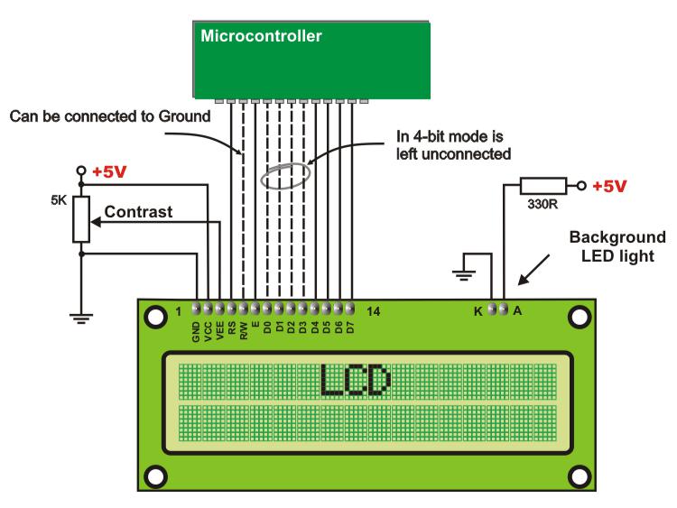
Fig 5.1: Interfacing of LCD to a micro controller
To send any command from table 2 to the LCD, make pin RS=0.
for data, make RS=1.Then send a high –to-low pulse to the E pin to enable the internal latch of the LCD.
CHAPTER-6
Description of Relays
6.1 Introduction
Relay is an electrically worked switch. Current moving through the loop of the hand-off makes an attractive field which pulls in a lever and changes the switch contacts. The curl current can be on or off so transfers have two switch positions and they are twofold toss (changeover) switches.
Transfers enable one circuit to switch a moment circuit which can be totally separate from the first. For instance a low voltage battery circuit can utilize a transfer to switch a 230V AC mains circuit. There is no electrical association inside the hand-off between the two circuits; the connection is attractive and mechanical.
The loop of a hand-off passes a moderately vast current, ordinarily 30mA for a 12V transfer, yet it can be as much as 100mA for transfers intended to work from lower voltages. Most ICs (chips) can’t give this current and a transistor is typically used to intensify the little IC current to the bigger esteem required for the transfer curl. The greatest yield current for the well known 555 clock IC is 200mA so these gadgets can supply hand-off curls specifically without enhancement.
Transfers are generally SPDT or DPDT yet they can have numerous more arrangements of switch contacts, for instance transfers with 4 sets of changeover contacts are promptly accessible. For additional data about switch contacts and the terms used to depict them please observe the page on switches.
Most transfers are intended for PCB mounting yet you can weld wires straightforwardly to the pins giving you take care to abstain from liquefying the plastic instance of the hand-off. The provider’s inventory ought to demonstrate to you the hand-off’s associations. The curl will be clear and it might be associated whichever way round. Hand-off curls deliver brief high voltage “spikes” when they are turned off and this can pulverize transistors and ICs in the circuit. To avert harm you should associate an assurance diode over the hand-off curl.
The enlivened picture demonstrates a working hand-off with its curl and switch contacts. You can see a lever on the left being pulled in by attraction when the loop is exchanged on. This lever moves the switch contacts. There is one arrangement of contacts (SPDT) in the frontal area and another behind them, making the hand-off DPDT.
The hand-off’s switch associations are generally marked COM, NC and NO:
• COM = Common, dependably associate with this, it is the moving some portion of the switch.
• NC = Normally Closed, COM is associated with this when the hand-off loop is off.
• NO = Normally Open, COM is associated with this when the transfer curl is on.
• Connect to COM and NO on the off chance that you need the changed circuit to be on when the transfer loop is on.
• Connect to COM and NC on the off chance that you need the changed circuit to be on when the hand-off curl is off.
Relay is an electrically operated switch. Current flowing through the coil of the relay creates a magnetic field which attracts a lever and changes the switch contacts. The coil current can be on or off so relays have two switch positions and they are double throw (changeover) switches.
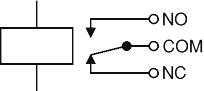
6.2 Protection diodes for transistors:
Transistors and ICs (chips) must be shielded from the concise high voltage “spike” created when the hand-off loop is turned off. The graph demonstrates how a flag diode (eg 1N4148) is associated over the transfer curl to give this security. Take note of that the diode is associated “in reverse” with the goal that it will ordinarily not direct. Conduction just happens when the transfer curl is turned off, right now current tries to keep moving through the loop and it is innocuously occupied through the diode. Without the diode no current could stream and the curl would deliver a harming high voltage “spike” in its endeavor to keep the currentflowing.
6.3 Comparison of Relays and transistors:
Like transfers, transistors can be utilized as an electrically worked switch. For exchanging little DC streams (
decision than a hand-off. However transistors can’t switch AC or high voltages, (for example, mains power) and they are not as a rule a decent decision for exchanging extensive streams (> 5A). In these cases a hand-off will be required, however take note of that a low power transistor may in any case be expected to switch the current for the hand-off’s curl! The fundamental favorable circumstances and drawbacks of transfers are recorded underneath:
Favorable circumstances of transfers:
• Relays can switch AC and DC, transistors can just switch DC.
• Relays can switch high voltages, transistors can’t.
• Relays are a superior decision for exchanging huge streams (> 5A).
• Relays can switch many contacts immediately.
Disadvantages of transfers:
• Relays are bulkier than transistors for exchanging little streams.
• Relays can’t switch quickly (with the exception of reed transfers), transistors can switch all the time.
• Relays utilize more power because of the present coursing through their loop.
• Relays require more present than many chips can give, so a low power transistor might be expected to switch the current for the transfer’s curl.
In this venture 4 transfers are utilized to interface 4 heaps of which 3 are Loads i.e. ordinary and crisis loads though the other one is to switch the Energy Meter.
lever moves the switch contacts. There is one set of contacts (SPDT) in the foreground and another behind them, making the relay DPDT.
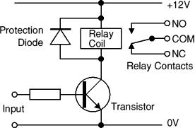
Fig:6.1 Relay circuit
CHAPTER-7
Description of Pumping System and Sensors
The Pumping System consists of a motor to pump the petrol into vehicles. The motor used is an a.c. motor. This motor is immersed into petrol. When a valid smart card is inserted into smart card reader with minimum balance, then after selecting the required no. of liters of petrol motor is powered through relative drivers by the microcontroller. Now the motor starts running and pours petrol into vehicle.
The driver circuitry involves a relay, an electro mechanical switch with a protection diode connected to it.
Fig:7.1 Sub-immersible pump
- FEATURES:
- Fully sub-immersible
- Completely noiseless
- Small size
- Continuous duty
- Long life
- Operates well at low voltage
- Self maintenance
- Operates well at low voltage
- Self maintenance
- Easily maintaining and cleaning
- SPECIFICATIONS:
- Operating voltage: 165-250v/50HZ
- Power: 16W
- H-max: 1.85 meters
- Output: 800L/h
- SAFETY PRECAUTIONS:
- Examine the pump after installation, it should not be plugged if there is water on part not intended to meet.
- Do not install where it will be exposed to the weather or to temperature below freezing.
A submersible pump (or electric submersible pump (ESP)) is a gadget which has a hermetically fixed engine close-coupled to the pump body. The entire get together is submerged in the liquid to be pumped. The fundamental favorable position of this sort of pump is that it averts pump cavitations, an issue related with a high rise distinction amongst pump and the liquid surface. Submersible pumps push fluid to the surface as opposed to jet pumps having to pull fluids.
7.4 Working principle:
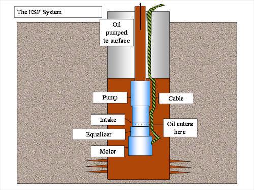
ESP frameworks are compelling for pumping created liquids to surface.The submersible pumps utilized as a part of ESP establishments are multistage outward pumps working in a vertical position. In spite of the fact that their constructional and operational elements experienced a ceaseless development throughout the years, their essential operational guideline continued as before. Created fluids, subsequent to being subjected to incredible radial powers brought about by the high rotational speed of the impeller, lose their motor vitality in the diffuser where a change of dynamic to weight vitality happens. This is the fundamental operational component of outspread and blended stream pumps. The pump shaft is associated with the gas separator or the defender by a mechanical coupling at the base of the pump. Well liquids enter the pump through an admission screen and are lifted by the pump stages. Different parts incorporate the outspread direction (bushings) conveyed along the length of the pole giving spiral support to the pump shaft turning at high rotational velocities. A discretionary push bearing takes up some portion of the hub powers emerging in the pump however the majority of those strengths are consumed by the defender’s pushed bearing.
7.5 Applications
Submersible pumps are found in numerous applications. Single stage pumps are utilized for waste, sewage pumping, general mechanical pumping and slurry pumping. They are likewise mainstream with aquarium channels. Numerous stage submersible pumps are ordinarily let down a borehole and utilized for water reflection, water wells and in oil wells.
Unique thoughtfulness regarding the sort of ESP is required when utilizing certain sorts of fluids. ESP’s ordinarily utilized on board maritime vessels can’t be utilized to dewater sullied overflowed spaces. These utilization a 440 volt A/C engine that works a little diffusive pump. It can likewise be utilized out of the water, bringing suction with a 2-1/2 inch non-collapsible hose. The pumped fluid is coursed around the engine for cooling purposes. There is a probability that the gas will spill into the pump bringing on a fire or decimating the pump, so boiling hot water and combustible fluids ought to be kept away from.
ESP use in oil wells
Submersible pumps are utilized as a part of oil generation to give a generally effective type of “simulated lift”, ready to work over a wide scope of stream rates and profundities. By diminishing the weight at the base of the well (by bringing down base opening streaming weight, or expanding drawdown), fundamentally more oil can be created from the well when contrasted and regular generation. The pumps are commonly electrically fueled and alluded to as Electrical subimmersible Pumps(ESP).
ESP frameworks comprise of both surface parts (housed in the generation office, for instance an oil stage) and sub-surface segments (found in the well opening). Surface segments incorporate the engine controller (regularly a variable speed controller), surface links and transformers. Subsurface parts normally incorporate the pump, engine, seal and links. A gas separator is here and there installed.The pump itself is a multi-arrange unit with the quantity of stages being controlled by the working prerequisites. Each stage comprises of a determined impeller and a diffuser which guides stream to the following phase of the pump. Pumps come in measurements from 90mm (3.5 inches) to 254mm (10 inches) and fluctuate between 1 meter (3 ft) and 8.7 meters (29 ft) long. The engine used to drive the pump is ordinarily a three stage, squirrel confine acceptance engine, with a nameplate control rating in the range 7.5 kW to 560 kW (at 60 Hz).New assortments of ESP can incorporate a water/oil separator which allows the water to be reinjected into the store without the need to lift it to the surface. Significant brands are Schlumberger’s Reda, Woodgroup’s ESP, Weatherford BORETS and Baker Hughes’ Centrilift. Up to this point, ESPs had been very exorbitant to introduce because of the necessity of an electric link downhole. This link must be wrapped around jointed tubing and associated at each joint. New snaked tubing umbilicals take into consideration both the channeling and electric link to convey with a solitary ordinary curled tubing unit.
The ESP framework comprises of various segments that turn an arranged arrangement of radiating pumps to build the weight of the well liquid and push it to the surface. The vitality to turn the pump originates from a high-voltage (3 to 5 kV) substituting current source to drive an uncommon engine that can work at high temperatures of up to 300 °F (149 °C) and high weights of up to 5,000 psi (34 MPa), from profound wells of up to 12,000 feet (3.7 km) profound with high vitality prerequisites of up to around 1000 strength (750 kW). ESPs have drastically bring down efficiencies with huge divisions of gas, more prominent than around 10% volume at the pump consumption. Given their high rotational speed of up to 4000 rpm (67 Hz) and tight clearances, they are not extremely tolerant of solids, for example, sand.
7.6 LIQUID LEVEL INDICATOR
Liquid level indicator is used to indicate the water present at what level. Here we are considering three level Low level .Medium level and High level, as the liquid level increases a message is sent to the concern person regard level of water.
7.7 SOIL MOISTURE SENSOR:
Features of the Soil moisture sensor:
- The circuit designed uses a 5V supply, fixed resistance of 100Ω, variable resistance of 10ΚΩ, two copper leads as the sensor probes, 2N222N transistor.
- It gives a voltage output corresponding to the conductivity of the soil.
- The conductivity of soil depends upon the amount of moisture present in it. It increases with increase in the water content of the soil.
- The voltage output is taken at the transmitter which is connected to a variable resistance. This variable resistance is used to adjust the sensitivity of the sensor.
Soil moisture sensor:
Practical description of Soil moisture sensor:
The two copper drives go about as the sensor tests. They are submerged into the example soil whose dampness substance is under test. The dirt is inspected under three conditions:
STEP1: Dry condition-The tests are put in the dirt under go conditions and are embedded away to a reasonable profundity of the dirt. As there is no conduction way between the two copper drives the sensor circuit stays open. The voltage yield of the producer for this situation ranges from 0 to 0.5V.
STEP2: Optimum condition-When water is added to the dirt, it permeates through the progressive layers of it and spreads over the layers of soil because of slender compel. This water expands the dampness substance of the dirt. This prompts an expansion in its conductivity which shapes a conductive way between the two sensor tests prompting a nearby way for the present spilling out of the supply to the transistor through the sensor tests. The voltage yield of the circuit taken at the producer of the transistor in the ideal case ranges from 1.9 to 3.4V around.
STEP3: Excess water condition-With the expansion in water content past the ideal level, the conductivity of the dirt increments radically and an unfaltering conduction way is set up between the two sensor leads and the voltage yield from the sensor builds no further past a specific point of confinement. The most extreme conceivable incentive for it is not more than 4.2V
CHAPTER-8
Description of RF Section
8.1 RF Transmitter section
RF transmitters are electronic gadgets that make ceaselessly shifting electric current, encode sine waves, and communicate radio waves. RF transmitters utilize oscillators to make sine waves, the least difficult and smoothest type of constantly fluctuating waves, which contain data, for example, sound and video. Modulators encode these sign spouses and recieving wires communicate them as radio signs. There are a few approaches to encode or adjust this data, including abundancy tweak (AM) and recurrence regulation (FM). Radio methods constrain confined impedance and clamor. With direct arrangement spread range, signs are spread over a vast band by multiplexing the flag with a code or mark that tweaks each piece. With recurrence jumping spread range, signals travel through a limited arrangement of directs in a consecutive, recurrent, and foreordained example.
Choosing RF transmitters requires a comprehension of balance strategies, for example, AM and FM. On-off key (OOK), the most straightforward type of balance, comprises of killing the flag on or. Plentifulness tweak (AM) causes the base band flag to change the sufficiency or stature of the transporter wave to make the coveted data content. Recurrence tweak (FM) causes the momentary recurrence of a sine wave transporter to withdraw from the inside recurrence by a sum relative to the prompt estimation of the regulating signal. Sufficiency move key (ASK) transmits information by differing the adequacy of the transmitted flag. Recurrence move key (FSK) is an advanced regulation plan utilizing at least two yield frequencies. Stage move key (PSK) is a computerized regulation plan in which the period of the transmitted flag is shifted as per the base band information flag.
Extra contemplations while choosing RF transmitters incorporate supply voltage, supply current, RF connectors, extraordinary elements, and bundling. Some RF transmitters incorporate visual or perceptible cautions or LED markers that flag working modes, for example, control on or gathering. Different gadgets append to coaxial links or incorporate a connector or port to which a radio wire can be joined. Normally, RF transmitters that are evaluated for open air utilize highlight an overwhelming obligation waterproof outline. Gadgets with inner adjustment and a recurrence extend switch are likewise accessible.
RF transmitters are utilized as a part of an assortment of utilizations and enterprises. Frequently, gadgets that are utilized with coordinated circuits (ICs) consolidate surface mount innovation (SMT), through gap innovation (THT), and level pack. In the broadcast communications industry, RF transmitters are intended to fit in a metal rack that can be introduced in a bureau. RF transmitters are additionally utilized as a part of radios and in electronic article observation frameworks (EAS) found in retail locations. Stock administration frameworks utilize RF transmitters as an other option to scanner tags.
8.1.1 RF transmitter ST-TX01-ASK:
General Description:
The ST-TX01-ASK is an ASK Hybrid transmitter module. The ST-TX01-ASK is designed by the Saw Resonator, with an effective low cost, small size, and simple-to-use for designing.
| | Frequency Range: | 315 / 433.92 MHZ. | |
| | Supply Voltage: | 3~12V. | |
| | Output Power: | 4~16dBm | |
| | Circuit Shape | : | Saw |
Applications
- Wireless security systems
- Car Alarm systems
- Remote controls.
- Sensor reporting
- Automation systems
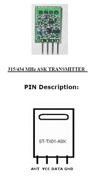
Fig 8.1: Pin Description of the Transmitter module
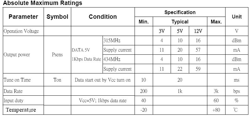
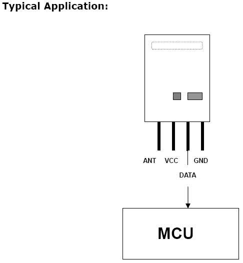
Fig 8.2: Interfacing TX module to a Micro controller
8.2 RF ENCODER (HT12E):
8.2.1 Features
- Operating voltage
- 2.4V~5V for the HT12A
- 2.4V~12V for the HT12E
- Low power and high noise immunity CMOS technology
- Low standby current: 0.1_A (typ.) at VDD=5V
- HT12A with a 38kHz carrier for infrared transmission medium
- Minimum transmission word
- Four words for the HT12E
- One word for the HT12A
- Built-in oscillator needs only 5% resistor
- Data code has positive polarity
- Minimal external components
- HT12A/E: 18-pin DIP/20-pin SOP package
8.2.2 Applications
- Burglar alarm system
- Smoke and fire alarm system
- Garage door controllers
- Car door controllers
- Car alarm system
- Security system
- Cordless telephones
- Other remote control systems
8.2.3 General Description
The 212 encoders are a progression of CMOS LSIs for remote control framework applications. They are equipped for encoding data which comprises of N address bits and 12_N information bits. Each address/information info can be set to one of the two rationale states. The modified locations/information are transmitted together with the header bits by means of a RF or an infrared transmission endless supply of a trigger flag. The capacity to choose a TE trigger on the HT12E or a DATA trigger on the HT12A additionally upgrades the application adaptability of the 212 arrangement of encoders. The HT12A also gives a 38kHz bearer to infrared frameworks.
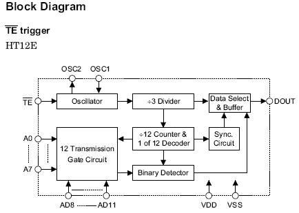
Fig 8.3: Block diagram of HT 12E Encoder
Pin Description:
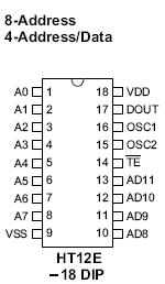
Fig 8.4: Pin description of HT12E
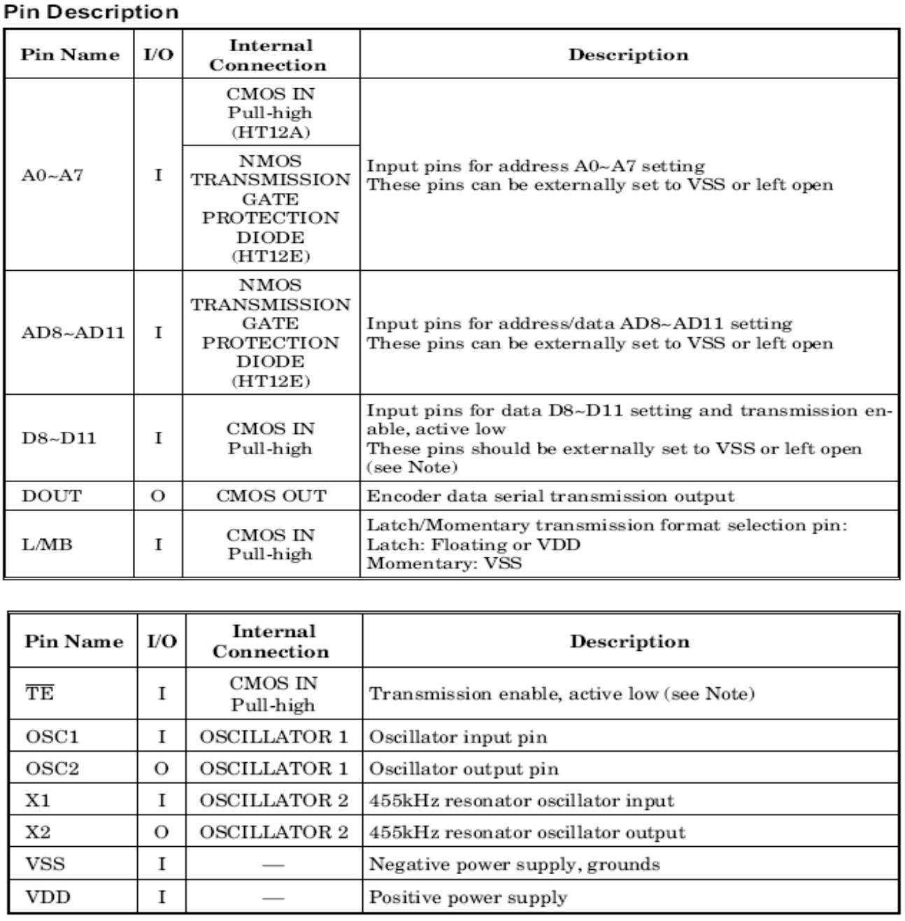
Note: D8~D11 are all data input and transmission enable pins of the HT12A.
TE is a transmission enable pin of the HT12E.
| 84 | |
| Absolute Maximum Ratings | |
| Supply Voltage (HT12A) | ………….._0.3V to 5.5V |
| Storage Temperature…………….. | _50_C to 125_C |
| Operating Temperature…………… | _20_C to 75_C |
| Supply Voltage (HT12E) …………… | _0.3V to 13V |
| Input Voltage……………….. | VSS_0.3 to VDD+0.3V |
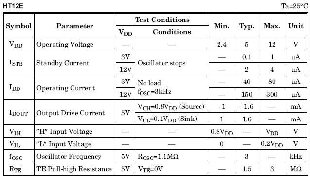
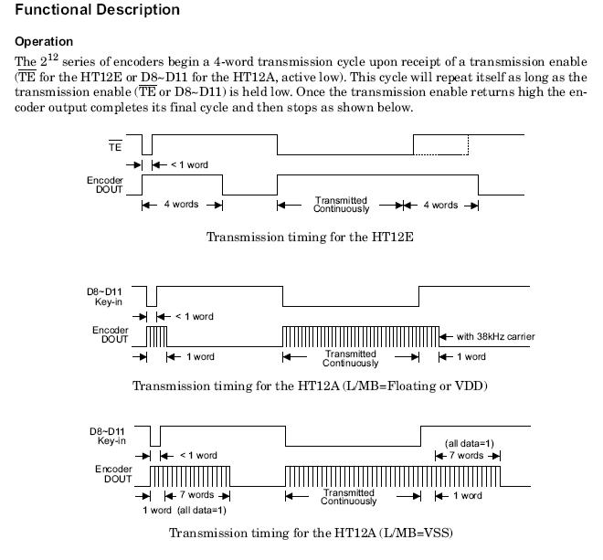
Fig 8.5: Timing diagram of the HT12E and HT12A
Flow Chart:
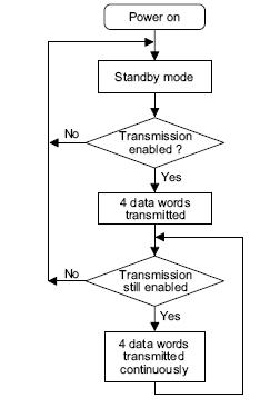
Fig 8.6: Flow chat for data transmission in HT12E
8.3 RF receiver section:
RF beneficiaries are electronic gadgets that different radio signs from each other and change over particular signs into sound, video, or information groups. RF beneficiaries utilize a recieving wire to get transmitted radio signs and a tuner to isolate a particular flag from the majority of alternate flags that the reception apparatus gets. Identifiers or demodulators then concentrate data that was encoded before transmission. There are a few approaches to disentangle or adjust this data, including abundancy tweak (AM) and recurrence balance (FM). Radio systems confine limited impedance and clamor. With direct succession spread range, signs are spread over a huge band by multiplexing the flag with a code or mark that tweaks each piece. With recurrence jumping spread range, signals travel through a restricted arrangement of diverts in a successive, recurrent, and foreordainedexample.
Choosing RF recipients requires a comprehension of regulation techniques, for example, AM and FM. On-off key (OOK), the least difficult type of balance, comprises of killing the flag on or. Sufficiency tweak (AM) causes the base band flag to fluctuate the plentifulness or stature of the transporter wave to make the coveted data content. Recurrence regulation (FM) causes the immediate recurrence of a sine wave transporter to leave from the middle recurrence by a sum corresponding to the quick estimation of the adjusting signal. Adequacy move key (ASK) transmits information by differing the sufficiency of the transmitted flag. Recurrence move key (FSK) is an advanced balance conspire utilizing at least two yield frequencies. Stage move key (PSK) is a computerized adjustment conspire in which the period of the transmitted flag is fluctuated as per the base band information flag.
RF beneficiaries fluctuate as far as execution particulars, for example, affectability, advanced inspecting rate, estimation determination, working recurrence, and correspondence interface. Affectability is the base information flag required to deliver a predetermined yield flag having a predefined flag to-clamor (S/N) proportion. Computerized inspecting rate is the rate at which tests can be drawn from an advanced flag in kilo tests every second. Estimation determination is the base advanced determination, while working recurrence is the scope of got signs. Correspondence interface is the technique used to yield information to PCs. Parallel interfaces incorporate broadly useful interface transport (GPIB), which is otherwise called IEEE 488 and HPIB Protocol. Serial interfaces incorporate all inclusive serial transport (USB), RS232, and RS485.
Extra contemplations while choosing RF recipients incorporate supply voltage, supply current, beneficiary information sources, RF connectors, uncommon components,
also, bundling. Some RF beneficiaries incorporate visual or capable of being heard alerts or LED pointers that flag working modes, for example, control on or gathering. Different gadgets join to coaxial links or incorporate a connector or port to which a reception apparatus can be appended. Normally, RF collectors that are appraised for open air utilize highlight a substantial obligation waterproof outline. Gadgets with inward adjustment and a recurrence run switch are likewise accessible.
- RF receiver ST-RX04-ASK: Description:
The RX04 is a low power ASK receiver IC which is fully compatible with the MitelKESRX01 IC and is suitable for use in a variety of low power radio applications including remote keyless entry. The RX04 is based on a single-Conversion, super-heterodyne receiver architecture and incorporates an entire phase-locked loop (PLL) for precise local oscillator generation.
- Applications:
- Car security system
- Wireless security systems
- Sensor reporting
- automation system
- Remote Keyless entry
8.3.3 Features
- Low power consumption.
- Easy for application.
- On-Chip VCO with integrated PLL using crystal oscillator reference.
- Integrated IF and data filters.
- Operation temperature range : ﹣10℃~+60℃
- Operation voltage: 5 Volts.
- Available frequency at : 315/434 MHz
8.3.4 Functional description:
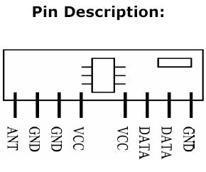
Fig 8.7: RF receiver module.
8.4 RF DECODER (HT 12D):
8.4.1 Features
Operating voltage: 2.4V~12V
Low power and high noise immunity CMOS technology Low standby current
Capable of decoding 12 bits of information
Binary address setting
Received codes are checked 3 times Address/Data number combination HT12D: 8 address bits and 4 data bits HT12F: 12 address bits only
Built-in oscillator needs only 5% resistor Valid transmission indicator
Easy interface with an RF or an infrared transmission medium Minimal external components
Pair with Holteks 212 series of encoders 18-pin DIP, 20-pin SOP package
8.4.2 Applications
Burglar alarm system
Smoke and fire alarm system
Garage door controllers
Car door controllers
Car alarm system
Security system
Cordless telephones
Other remote control systems
8.4.3 General Description
The 212 decoders are a series of CMOS LSIs for remote control system applications. They are paired with Holteks 212 series of encoders (refer to the encoder/decoder cross reference table). For proper operation, a pair of also, bundling. Some RF beneficiaries incorporate visual or capable of being heard alerts or LED pointers that flag working modes, for example, control on or reception.encoder/decoder with a similar number of locations and information configuration ought to be picked. The decoders get serial locations and information from a customized 212 arrangement of encoders that are transmitted by a transporter utilizing a RF or an IR transmission medium. They think about the serial information three times ceaselessly with their residential locations. In the event that no mistake or unmatched codes are found, the information codes are decoded and after that exchanged to the yield pins. The VT stick likewise goes high to demonstrate a legitimate transmission. The 212 arrangement of decoders are fit for interpreting informations that comprise of N bits of address and 12_N bits of information. Of this arrangement, the HT12D is organized to give 8 address bits and 4 information bits, and HT12F is utilized to disentangle 12 bits of deliver information.Other gadgets join to coaxial links or incorporate a connector or port to which a radio wire can be appended. Commonly, RF collectors that are evaluated for open air utilize highlight a substantial obligation waterproof plan. Gadgets with inward adjustment and a recurrence run switch are additionally accessible.
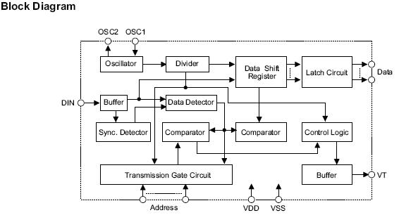
Fig 8.8: Block Diagram of HT 12D Decoder
Note: The address/data pins are available in various combinations (see the address/data table).
Pin Assignment:
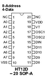
Fig 8.9: Pin diagram of HT12D
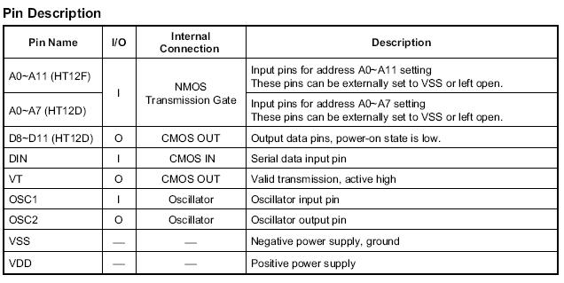
| Absolute Maximum Ratings | |
| Supply Voltage …………………………………… | _0.3V to 13V |
| Storage Temperature ………………………. | _50_C to 125_C |
| Input Voltage ………………………….. | VSS_0.3 to VDD+0.3V |
| Operating Temperature……………………… | _20_C to 75_C |
8.4.4Functional Description
Operation
The 212 arrangement of decoders gives different blends of locations and information sticks in various bundles in order to combine with the 212 arrangement of encoders. The decoders get information that are transmitted by an encoder and decipher the primary N bits of code period as locations and the last 12_N bits as information, where N is the address code number. A flag on the DIN stick enacts the oscillator, which thus deciphers the approaching location and information. The decoders will then check the got address three times persistently. On the off chance that the got address codes all match the substance of the decoders residential location, 12_N bits of information are decoded to actuate the yield pins and the VT stick is set high to show a legitimate transmission. This will last unless the address code is wrong or no flag is gotten. The yield of the VT stick is high just when the transmission is substantial. Else it is constantly low.
output type
 output type of the 212 arrangement of decoders, the HT12F has no information yield stick however its VT stick can be utilized as a fleeting information yield. The HT12D, then again, gives 4 lock sort information sticks whose information stay unaltered until new information are gotten.
Fig 8.10: Timing Diagram of Decoder HT12D
Flowchart
The oscillator is disabled in the standby state and activated when a logic _high_ signal applies to the DIN pin. That is to say, the DIN should be kept low if there is no signal input.
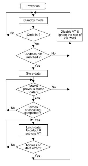
Fig 8.11: Flow chart of HT12D for data transmission
CHAPTER-9
SOFTWARE COMPONENTS:
Software used:
*Keil software for c programming
9.1 ABOUT KEIL SOFTWARE:
It is conceivable to make the source records in a content tool, for example, Notepad, run the Compiler on every C source document, determining a rundown of controls, run the Assembler on every Assembler source document, indicating another rundown of controls, run either the Library Manager or Linker (again determining a rundown of controls) lastly running the Object-HEX Converter to change over the Linker yield record to an Intel Hex File. Once that has been finished the Hex File can be downloaded to the objective equipment and fixed. Then again KEIL can be utilized to make source documents; naturally incorporate, connection and clandestine utilizing choices set with a simple to utilize UI lastly recreate or perform investigating on the equipment with access to C factors and memory. Unless you need to utilize the tolls on the charge line, the decision is clear. KEIL Greatly disentangles the way toward making and testing an inserted application.
9.2 Projects:
The client of KEIL focuses on ―projects‖. A venture is a rundown of all the source records required to construct a solitary application, all the apparatus choices which indicate precisely how to fabricate the application, and – if required – how the application ought to be mimicked. A venture contains enough data to take an arrangement of source records and produce precisely the paired code required for the application. In light of the high level of adaptability required from the devices, there are numerous choices that can be set to design the instruments to work in a particular way. It is dull to need to set these choices up each time the application is being manufactured; in this manner they are put away in a venture record. Stacking the venture record into KEIL illuminates KEIL which source documents are required, where they are, and how to arrange the devices in the right way. KEIL can then execute each instrument with the right alternatives. It is additionally conceivable to make new undertakings in KEIL. Source records are added to the venture and the instrument alternatives are set as required. The venture can then be spared to safeguard the settings. The venture is reloaded and the test system or debugger began, all the coveted windows are opened. KEIL extend documents have the expansion
9.3 Simulator/Debugger:
The test system/debugger in KEIL can play out an exceptionally point by point recreation of a small scale controller alongside outer signs. It is conceivable to see the exact execution time of a solitary gathering guideline, or a solitary line of C code, as far as possible up to the whole application, just by entering the precious stone recurrence. A window can be opened for every fringe on the gadget, demonstrating the condition of the fringe. This empowers snappy investigating of mis-designed peripherals. Breakpoints might be determined to either gathering directions or lines of C code, and execution might be ventured through one guideline or C line at once. The substance of all the memory ranges might be seen alongside capacity to discover particular factors. Furthermore the registers might be seen permitting a nitty gritty perspective of what the microcontroller is doing anytime.
The Keil Software 8051 improvement devices recorded underneath are the projects you use to incorporate your C code, amass your constructing agent source documents, connect your program together, make HEX documents, and troubleshoot your objective program. µVision2 for Windows™ Integrated Development Environment: joins Project Administration, Source Code Editing, and Program Debugging in one intense condition.
C51 ANSI Optimizing C Cross Compiler: makes relocatable question modules from your C source code,
A51 Macro Assembler: creates relocatable object modules from your 8051 constructing agent source code,
BL51 Linker/Locator: joins relocatable protest modules made by the compiler and constructing agent into the last outright question module,
LIB51 Library Manager: consolidates question modules into a library, which might be utilized by the linker,
OH51 Object-HEX Converter: makes Intel HEX records from supreme protest modules.
What’s New in µVision3?
µVision3 adds numerous new elements to the Editor like Text Templates, Quick Function Navigation, and Syntax Coloring with prop high lighting Configuration Wizard for discourse based startup and debugger setup. µVision3 is completely good to µVision2 and can be utilized as a part of parallel with µVision2.
What is µVision3?
µVision3 is an IDE (Integrated Development Environment) that helps you compose, order, and investigate implanted projects. It typifies the accompanying segments:
- A project manager.
- A make facility.
- Tool configuration.
- Editor.
- A powerful debugger.
To help you get started, several example programs (located in the
C51Examples, C251Examples, C166Examples, and ARM…Examples)
are provided.
- HELLO is a simple program that prints the string “Hello World” using theSerial Interface.
- MEASURE is a data acquisition system for analog and digital systems.
- TRAFFIC is a traffic light controller with the RTX Tiny operatingsystem.
- SIEVE is the SIEVE Benchmark.
- DHRY is the Dhrystone Benchmark.
- WHETS is the Single-Precision Whetstone Benchmark.
Additional example programs not listed here are provided for each device
architecture.
Building an Application in µVision2
To build (compile, assemble, and link) an application in µVision2, you must:
- Select Project -(forexample,166EXAMPLESHELLOHELLO.UV2).
- Select Project – Rebuild all target files or Build target.
µVision2 compiles, assembles, and links the files in your project
9.4 CPU Simulation:
µVision2 simulates up to 16 Mbytes of memory from which areas can be mapped for read, write,or code execution access. The µVision2 simulator traps and reports illegal memory accesses.
In addition to memory mapping, the simulator also provides support for the Integrated peripherals of the various 8051 derivatives. The on-chip peripherals of the CPU you have selected are configured from the Device.
Database selection:
you have made when you create your project target. Refer to page 58 for more Information about selecting a device. You may select and display the on-chip peripheral components using the Debug menu. You can also change the aspects of each peripheral using the controls in the dialog boxes.
Start Debugging:
You start the debug mode of µVision2 with the Debug – Start/Stop Debug Session command. Depending on the Options for Target – Debug Configuration, µVision2 will load the application program and run the startup code µVision2 saves the editor screen layout and restores the screen layout of the last debug session. If the program execution stops, µVision2 opens an editor window with the source text or shows CPU instructions in the disassembly window. The next executable statement is marked with a yellow arrow. During debugging, most editor features are still available.
For example, you can use the find command or correct program errors. Program source text of your application is shown in the same windows. The µVision2 debug mode differs from the edit mode in the following aspects:
_ The ―Debug Menu and Debug Commands‖ described on page 28 are
Available. The additional debug windows are discussed in the following. _ The project structure or tool parameters cannot be modified. All build Commands are disabled.
Disassembly Window
The Disassembly window shows your target program as mixed source and assembly program or just assembly code. A trace history of previously executed instructions may be displayed with Debug – View Trace Records. To enable the trace history, set Debug – Enable/Disable Trace Recording.
If you select the Disassembly Window as the active window all program step commands work on CPU instruction level rather than program source lines. You can select a text line and set or modify code breakpoints using toolbar buttons or the context menu commands.
You may use the dialog Debug – Inline Assembly… to modify the
CPU instructions. That allows you to correct mistakes or to make temporary changes to the target program you .
9.5Embedded C:
Data Types:
U people have already come across the word ―Data types‖ in C-Language. Here also the functionality and the meaning of the word is same except a small change in the prefix of their labels. Now we will discuss some of the widely used data types for embedded C- programming.
| Data Types | Size in Bits | Data Range/Usage | ||
| unsigned char | 8-bit | 0-255 | ||
| signed char | -128 to +127 | |||
| 8-bit | ||||
| unsigned int | 16-bit | 0 to 65535 | ||
| signed int | 16-bit | -32,768 to +32,767 | ||
| Sbit | 1-bit | SFR | bit | addressable |
| only | ||||
| Bit | 1-bit | RAM | bit | addressable |
| only | ||||
| Sfr | 8-bit | RAM | addresses 80- | |
| FFH only | ||||
Unsignedchar:The unsigned char is an 8-bit data type that takes a value in therange of 0-255(00-FFH). It is used in many situations, such as setting a counter value, where there is no need for signed data we should use the unsigned char instead of the signed char. Remember that C compilers use the signed char as the default if we do not put the key word
Signed char:
The signed char is an 8-bit data type that uses the most significant bit (D7 of D7-D0) to represent the – or + values. As a result, we have only 7 bits for the magnitude of the signed number, giving us values from -128 to +127. In situations where + and – are needed to represent a given quantity such as temperature, the use of the signed char data type is a must.
Unsigned int:
The unsigned int is a 16-bit data type that takes a value in the range of 0 to 65535 (0000-FFFFH). It is also used to set counter values of more than 256. We must use the int data type unless we have to. Since registers and memory are in 8-bit chunks, the misuse of int variables will result in a larger hex file. To overcome this we can use the unsigned char in place of unsigned int.
Signed int:
Signed int is a 16-bit data type that uses the most significant bit (D15 of D15-D0) to represent the – or + value. As a result we have only 15 bits for the magnitude of the number or values from -32,768 to +32,767.
Sbit (single bit):
The sbit data type is widely used and designed specifically to access single bit addressable registers. It allows access to the single bits of the SFR registers.
CHAPTER-10
CONCLUSION
The venture ―AUTOMATIC IRRIGATION WATER SUPPLY MONITORING AND CONTROL SYSTEM‖ has been effectively composed and tried.
It has been produced by coordinating elements of all the equipment parts utilized. Nearness of each module has been contemplated out and put deliberately consequently adding to the best working of the unit.
Besides, utilizing exceptionally propelled IC’s and with the assistance of developing innovation the venture has been effectively executed.
Future Enhancement
The application for engine pump based water system in agribusiness, by utilizing RTC we set the time and show in the LCD. We can set the time term of the pump to ON/OFF. The pump is exchanged ON consistently is put away, after consummation time span the pump is OFF.
For the most part continuous power cuts and deficient downpours at different phases of development are one of real reasons for misfortunes to ranchers. Numerous agriculturists utilize enlistment engine pumps to water their ranches from wells. In this application, GSM modem gets any approaching SMS message is specifically steered to miniaturized scale controller and any friendly instant message is straightforwardly sent by smaller scale controller to assigned wireless number without being put away in charge framework phone memory.
CHAPTER-11
REFERENCES
The following are the references made during the development of this project. [1] Raj Kamal, ―The concepts and Features of Micro-controllers‖,TataMcGraw
Hill,2008.
[ 2] Kenneth J Ayala, ―The 8051 Micro-controller Architecture, programming &Applications‖,West publishing company,1991.
[3]MykePredko, ― Programming and Customizing the 8051 Micro-controller‖,Tab books,1999.
[4]Mohd.Mazidi, ―8051-Microcontroller and Embedded System‖,Prentice
Hall,1999.
[5]David.E.Simon, ―Embedded Software Primer‖,Addison-Wesley Professional,1999.
NAME OF THE SITES
APPENDIX-1
MICROCONTROLLER PROGRAMME IN EMBEDDED C
TRANSMITTER SECTION:
#include
#include
sbit soil = P2^0; sbit lvl1 = P2^1; sbit lvl2 = P2^2;
sbit D0 = P1^0; sbit D1 = P1^1; sbit D2 = P1^2; sbit D3 = P1^3;
void main()
{
bitsoil_flg; soil=lvl1=lvl2=1;
soil_flg=0; D0=D1=D2=D3=1;
lcd_init(); delay(200);
disp_loc(0x80,”AUTOMATIC IRRIGA”);
disp_loc(0xc0,”SOIL & WATER LEV”); delay(500);
lcd_cmd(0x01);
disp_loc(0x80,” SOIL LVL1 LVL2 “); delay(100);
while(1)
{
if(soil==0)
{
disp_loc(0xc1,”WET “);// WET SO MOTOR IN OFF
CONDITION //
D3=D2=D1=1;D0=1;
}
else
{
soil_flg=1;
disp_loc(0xc1,”DRY”); // DRY SO MOTOR IN ON CONDITION // D3=D2=D1=1;D0=0;
}
if(soil_flg==1)
{
if(lvl1==1 && lvl2==1) // COMPARING OF
lvl1 && lvl2 //
{
D3=D2=D0=1;D1=0;
lcd_cmd(0xc6);
disp_str(” OFF OFF “);
}
if( lvl1==0 && lvl2==1) //
COMPARING OF lvl1 && lvl2 //
{
D3=D2=1;D1=0;D0=0; lcd_cmd(0xc6);
disp_str(” ON OFF “);
}
if(lvl1==0 && lvl2==0) // COMPARING OF lvl1 && lvl2 //
{
D3=D1=D0=1;D2=0;//motor=0; lcd_cmd(0xc6);
disp_str(” ON ON “);
}
if(lvl1==1 && lvl2==0) // COMPARING OF lvl1 && lvl2 //
{
D3=D1=1;D2=D0=0;//motor=1; lcd_cmd(0xc6);disp_str(” OFF ON”);
}
if(lvl1==0 && lvl2==1 && soil_flg1==1) // COMPARING OF lvl1 && lvl2 &&soil_flg //
{
D3=D0=1;D2=D1=0;//motor=0; lcd_cmd(0xc6);
disp_str(” ON OFF “);
}
}
}
}
RECEIVER SECTION:
#include
#include
sbit D0=P1^0; sbit D1=P1^1; sbit D2=P1^2; sbit D3=P1^3;
void main() {s
D0=D1=D2=D3=1;
motor=0; lcd_init();
delay(200);
disp_loc(0x80,”AUTOMATIC IRRIGA”); disp_loc(0xc0,”SOIL & WATER LEV”);
delay(500);
lcd_cmd(0x01);
disp_loc(0x80,” SOIL LVL1 LVL2 “); delay(100);
while(1)
{
if(D0==1 && D1==1 && D2==1 && D3==1)
{
disp_loc(0xc1,”WET “); // WET SO MOTOR IN OFF
CONDITION //
motor=0;
}
if(D0==0 && D1==1 && D2==1 && D3==1)
{
disp_loc(0xc1,”DRY”);//DRY SO MOTOR IN ON CONDITION// motor=0;
}
if(D0==1 && D1==0 && D2==1 && D3==1)
{
motor=1; lcd_cmd(0xc1);
disp_str(“DRY OFF OFF “);
}
if(D0==0 && D1==0 && D2==1 && D3==1)
{
motor=1; lcd_cmd(0xc1);
disp_str(“DRY ON OFF “); // CONTINOUS LOOP ///
}
if(D0==1 && D1==1 && D2==0 && D3==1)
{
motor=0; lcd_cmd(0xc1);
disp_str(“DRY ON ON “);
}
if(D0==0 && D1==1 && D2==0 && D3==1)
{
motor=1; lcd_cmd(0xc1);
disp_str(“DRY OFF ON “); } if(D0==1 && D1==0 && D2==0 && D3==1)
{
motor=0;
lcd_cmd(0xc1);
disp_str(“DRY ON OFF “);
}
}
}
Cite This Work
To export a reference to this article please select a referencing stye below:
Related Services
View all


Related Content
All TagsContent relating to: "Technology"
Technology can be described as the use of scientific and advanced knowledge to meet the requirements of humans. Technology is continuously developing, and is used in almost all aspects of life.
Related Articles

DMCA / Removal Request
If you are the original writer of this dissertation and no longer wish to have your work published on the UKDiss.com website then please: