Digital Clock Design with FPGA Board
Info: 14746 words (59 pages) Dissertation
Published: 3rd Dec 2021
Tagged: Computer Science
CHAPTER 1: Introduction
1.1 Aim of the Project
The main objective of the digital clock is to display the time digitally using 7-segment display on Artix-7 FPGA Board. The digital clock by default displays the run time and time can be set by using time set assigned to switch on board. The feature like alarm is also set by using alarm set and alarm on switch assigned on kit. The digital clock designed is a 24-clock hour format. It displays the time in format of hours:minutes: seconds.
1.2 Literature Survey
The advances in digital technology have been phenomenal over the years and that giving birth to digital system design which continue to serve as a great source of succour and comfort to mankind in many ways. These days, numerous applications in Electronics and other technologies are using digital techniques to perform operations that were once performed by analogue methods. The digital systems owe the versatility and superiority over analogue methods to the fact that they do not get affected by spurious fluctuations in voltage; have greater precision and accuracy; and can store billions of bits of information in a relatively small space. Several authors have made different researches to minimize the power requirements in manufacturing an integrated chip and to have high flexibility and performance. The development of FPGA board is a part of the research.
The research paper “Basics of field programmable gate arrays” by Waqar Hussian stated the need of FPGA(field programmable gate array) when compared to other programmable logic devices. It also stated the future scope of FPGA and its applications. It gave a clear description of internal architecture of FPGA and its related hardware description language.It also explained about the design flow of like synthesis ,place, routing etc.. The importance of timing ,area, power analysis is also explained. From this paper we can understand clearly about FPGA.
The paper FPGA-based Implementation of Digital Logic Design using Altera DE2 Board depicts the clear picture of significance of FPGA .The paper focuses that in control applications, most of the physical systems require a real-time operation to interface high speed constraints; higher density programmable logic devices such as field programmable gate array (FPGA) can be used to integrate large amounts of logic in a single IC. This paper presents an Experimental implementation of digital logic designs on the Altera DE2 board which presented as an educational and development board, in order to check the flexible implementation with FPGA and to get the better and safely ways to use these specifications during any design implementations. The report made from FPGA tutorial “Over view on FPGA” states that FPGA provides its user a way to configure and these specifications offer the fuzzy logic a large amount of logic in single IC: The intersection between the logic blocks and the function of each logic block. Logic block of an FPGA can be configured in such a way that it can provide functionality as simple as that of transistor or as complex as that of a microprocessor. It can used to implement different combinations of combinational and sequential logic functions.
The research paper by Parth Mehta shows the reports of designing a simple digital clock on spartan3 FPGA kit. The digital clock displays the time only in minutes and seconds with more delay .Out of total 4MHz,it used only 1hz frequency with 22 bit register. It uses the already existing blocks like counter, decoder, multipier. From this paper we can improve some things like instead of displaying only secs and mins we can display total hrs,mins,secs. We can also generate a clock with more frequency from the default frequency of the kit. Thus we can have more enhanced digital clock with alarm.
CHAPTER 2: Overview of Implementation and Prototype Verification of Digital Clock Using FPGA
2.1 Introduction
This project makes use of FPGA for the hardware implementation of digital clock. As soon as the FPGA is switched on, the clock starts. The FPGA and on board clock will generate the timing signals. The clock time and alarm time can be set using the dip switches on the board. The proposed digital clock design is enhanced using the digital operations: counting, comparing, incrementing and decrementing. The clock time can be set using timeset switch and the alarm time can be set using alarmset switch. The alarm will be on when clock time is equal to alarm time. Minutes and hours can be incremented and decremented by using the push buttons on the board.
One second signal is generated using the global clock and then this seconds clock is used to generate the timing signals. It consists of six registers in total which includes hr2,hr1,min2,min1,sec2,sec1. When sec1 is 9 and sec2 is 5, then sec2 and sec1 values are made to zero and min1 value is incremented. If min2 is 5 and min1 is 9 then min2 and min1 values are made to zero and hr1 is incremented. If hr2 is 2 and hr1 is 4 then hr2 and hr1 is made to zero and thus the count continues.
2.2 Design Flow of Digital Clock
The VLSI design cycle is a formal specification of a VLSI chip which follows a series of steps and finally produces a packaged chip. A model design cycle may be represented by the flow chart shown in Figure 2.1. Our attention is on the physical design step of the VLSI design cycle. However, to gain a global approach, we briefly outline all the steps of the VLSI design cycle.
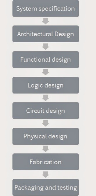
Figure 2.1: VLSI Design flow
1. System Specification
The initial step of any design process is to lay down the specifications of the system. It is a high level representation of the system. The factors to be considered in this process are performance, functionality, and physical dimensions.
2. Architectural Design
- The architecture of the system designed in this step will be basic. Itincludes such decisions as RISC (Reduced Instruction Set Computer) versus CISC (Complex Instruction Set Computer), number of ALUs, Floating Point units, number and structure of pipelines, and size of caches among others.
- The outcome of the architectural design is a Micro-Architectural Specification (MAS). While MAS is a textual (English like) description, architects can accurately predict the power, performance and die size of the design based on such a description.
3. Behavioral or Functional Design
- The behavioral aspects of the system are however considered without implementation specific information. For example, it may specify that a multiplication is required, but exactly in which mode such multiplication may be executed is not specified. We may use a wide variety of multiplication hardware depending on the speed and word size requirements. The key idea is to specify behavior, in terms of input, output and timing of each unit, without specifying its internal structure.
- The outcome of the functional design is a timing diagram or other relationships betweenunits. This information leads to improvement of the overall design process and reduction of the complexity of subsequent phases. Functional or behavioral design allows quick emulation of the system and allows fast debugging of the full system. Behavioral design is largely a manual step with little or no automation help available.
4. Logic Design
In this step the control flow, word widths, register allocation, arithmetic operations and logic operations of the design that represent the functional design are derived and tested.
5. Circuit Design
The main purpose of circuit design is to develop a circuit representation based on the logic design. The Boolean expressions are converted into a circuit representation by taking the speed and power requirements of the original design into consideration. Circuit Simulation is used to verify the timing and correctness of each component.
6. Physical Design
In this step the netlist (or circuit representation) is converted into a geometric representation. As stated earlier, this geometric representation of any circuit is called a layout. Layout thus created by converting each logic component (gates, macros, transistors and cells) into a geometric representation (specific shapes in multiple layers), will perform the intended logic function of the corresponding component. Connections between different components are even expressed as geometric patterns as lines in multiple layers.
7. Fabrication
After verification and layout, the design is ready for fabrication. Since layout data is sent to fabrication on a tape, the process of release of data is called Tape Out. Layout data is then converted (or fractured) into photo-lithographic masks, one for each layer. Masks identify spaces on the wafer, where certain materials need to be deposited, diffused or even removed. Silicon crystals are grown and sliced to further produce wafers. Extremely small dimensions of VLSI devices require the wafers to be polished to near perfection. The fabrication process consists of several steps involving deposition and diffusion of different materials on the wafer. During each step one mask is used. Several masks may be used to complete the process of fabrication.
8. Packaging, Testing and Debugging
Finally, the wafer is fabricated and diced into distinct chips in a fabrication facility. Each chip is then packaged and tested to ensure that it meets all the required design specifications and also that it functions properly. Chips used in Printed Circuit Boards (PCBs) are packaged in Ball Grid Array (BGA), Pin Grid Array (PGA), Dual In-line Package (DIP), and Quad Flat Package (QFP). Chips used in Multi-Chip Modules (MCM) are not packaged, since MCMs use bare or naked chips.
2.3 Hardware Requirements
The hardware requirements for the implementation and prototype verification of digital clock using FPGA is the Artix-7 Nexys4 board of FPGA.
The FPGA arrangement, specified using HDL is similar to the one used for the application specific IC (ASIC) (to specify the configuration circuit diagrams were used previously, as they were for ASICs, which is rare now). We use Digital clock to display the time digitally. Earlier, the power analysis was done by using hardware components which was very complex. If any component is not working or is to be changed in circuitry whole circuit is to be replaced. This problem got resolved by software analysis of power using Xilinx ISE 14.2XPower analyzer. With the help of XPower analyzer we can change the value of different components such as capacitance, current, voltage, temperature.
The Nexys4 DDR board is a complete, ready-to-use digital circuit development platform based on the latest Artix-7 Field Programmable Gate Array (FPGA) from Xilinx. With its(XC7A100T-1CSG324C) high-capacity, generous external memories, collection of USB and various other ports, the Nexys4 DDR hosts designs that ranges from introductory combinational circuits to the most powerful embedded processors which is an added advantage. The Nexys4 DDR board can be used for a wide range of designs because of the several built-in peripherals like accelerometer, temperature sensor, MEMs digital microphone, speaker amplifier and I/O devices.
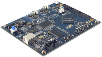
Figure 2.2 :FPGA board
2.4 Software Requirements
The software requirements for the implementation and prototype verification of digital clock using FPGA are Vivado 16.2 design tool and Verilog HDL.
The Vivado Design Suite is designed to improve productivity. This entire new design tool suite is architected to increase the overall productivity for designing, integrating and implementing with the Xilinx 7 series, Zynq- 7000 All Programmable and Ultra Scale devices. With the Vivado 16.2, you can enhance design implementation with place and route tools which logically optimizes for multiple and concurrent design metrics. The design metrics can be timing, congestion, total wire length, utilization and power. The total design process which is built on the shared scalable data model of Vivado Design Suite can be easilyexecuted in memory without having to write ortranslate any intermediate file formats. It also accelerates debug and implementation, runtimes while minimizing memory requirements. The Vivado Design Suite provides you with design analysis capabilities at every design stage. This allows for design and tool setting modifications earlier in the design processes where they have less overall schedule impact, thus minimizing design iterations and increasing productivity.
All the Vivado Design Suite tools are written with a native tool command language (Tcl) interface. All the options and commands available in the Vivado Integrated Design Environment (IDE), which is the Graphical User Interface (GUI) for the Vivado Design Suite, are easily accessible through Tcl. The Vivado Design Suite also provides powerful access to the design data for configuration and reporting as well as theoptions and tool commands.
Verilog HDL is a hardware description language which can be used to design and document electronic systems. Verilog HDL allows designers to design at different levels of abstraction. It is the most widely used HDL that has a user community of more than 50,000 active designers.Verilog-HDL allows you to describe the design at different levels of abstractions within a design like Behavioral level, RTL level, Gate level, Switch Level. Verilog modules are basic building blocks in hierarchy.
CHAPTER 3: Implementation with FPGA
3.1 Introduction
The group of Spartan-3 FPGA (Field-Programmable Gate Arrays) is intended to deal with the necessities of cost-touchy and high volume shopper electronic applications. The Spartan-3 family expands on the accomplishment of the prior Spartan-IIE family by expanding the limit of interior RAM, the aggregate number of I/Os, the measure of rationale assets and the general level of execution and additionally by enhancing clock administration capacities. In light of their outstandingly minimal effort, Spartan-3 FPGAs are preferably suited to an extensive variety of buyer gadgets applications including broadband get to, home systems administration, show/projection and advanced TV gear.
The Spartan-3 family is an option for veiling customized ASICs. FPGAs are better over ASICs in light of the fact that they dodge the long improvement cycles, the natural rigidity and the high beginning expense. FPGA programmability additionally allows configuration updates in the field with no equipment replacement, an impossibility with ASICs.
3.1.1 Features
Select IO™ flagging
- Up to 784 I/O pins
- 622 Mb/s information exchange rate per I/O
- 18 single-finished flag principles
- 8 differential I/O gauges including LVDS, RSD
- Termination by Digitally Controlled Impedance
- Signal swing running from 1.14V to 3.45V
- Double Data Rate (DDR) bolster
- DDR, DDR2 SDRAM bolster up to 333 Mbps
Low-cost, elite rationale answer for high-volume, shopper arranged applications
Densities up to 74,880 rationale cells
Logic assets
- Abundant rationale cells with move enlist capacity
- Wide, quick multiplexers
- Fast look-ahead convey rationale
- Dedicated 18 x 18 multipliers
- JTAG rationale perfect with IEEE 1149.1/1532
Select RAM™ progressive memory
- Up to 1,872 Kbits of aggregate square RAM
- Up to 520 Kbits of aggregate disseminated RAM
Digital Clock Manager (up to four DCMs)
- Clock skew end
- Frequency union
- High determination stage moving
Eight worldwide clock lines and bottomless directing
Fully bolstered by Xilinx ISE advancement framework
Synthesis, mapping, arrangement and directing
Micro Blaze processor, PCI, and different centers
sans pb bundling alternatives
Low-control Spartan-3L Family and Automotive Spartan-3 XA Family variations
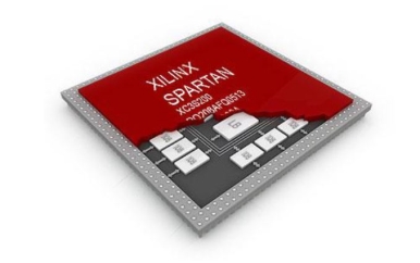
Figure 3.1 : Xilinx Spartan series
3.2 Architectural Overview
The architecture of Spartan-3 family consists of the following fundamental programmable functional elements:
Configurable Logic Blocks (CLBs)
It contain RAM-based Look-Up Tables (LUTs) to implement logic and storage elements which can be used as flip-flops or latches. CLBs can be programmed to perform a large variety of logical functions as well as to store data.
Input-Output Blocks (IOBs)
It control the flow of data between the Input/Output pins and the internal logic of the device. Each block supports 3-state operation and bidirectional data flow. There are Twenty-four different signal standards, including seven high-performance differential standards. Double Data-Rate (DDR) registers are also included.
Block RAM
It provides data storage in the form of 18-Kbit dual-port blocks.
Multiplier blocks
It will accept two 18-bit binary numbers as inputs and then calculates the product.
Digital Clock Manager (DCM)
It give self-adjusting, completely computerized answers for conveying, postponing, duplicating, partitioning, and stage moving clock signals. A ring ofIOBs encompasses a variety of CLBs.
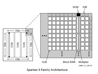
Figure 3.2 :Spartan 3E family architecture
3.2.1 Configurable Logic Blocks (CLB’s)
The Configurable Logic Blocks (CLBs) are the main logic resources for implementing both synchronous and combinational circuits. Each CLB comprises four interconnected slices. These slices are grouped in pairs. Each pair of slice is organized as a column with an independent carry chain.
- Local routing provides feedback between slices in the same CLB, and it provides routing to neighboring CLBs
- A switch matrix provides access to general routing resources
- Each slice has four outputs
- Two registered outputs, two non-registered outputs
- Two BUFTs associated with each CLB, accessible by all 16 CLB outputs
Figure 3.3 : Configurable Logic Blocks
3.2.2 Look Up Tables
Combinational logic is stored in Look-Up Tables (LUTs)
– Also called Function Generators
– The Capacity is limited by the number of inputs, not by the complexity
• Delay through the LUT is constant
The RAM-based function generator also known as a Look-Up Table or LUT is the main resource for implementing logic functions. Furthermore, the LUTs in each left-hand slice pair can be configured as Distributed RAM or a 16-bit shift register.
Among other uses, the storage element, which is programmable as either a D-type flip-flop or a level-sensitive latch, synchronizes data to a clock signal.
The storage elements in the upper and lower portions of the slice are called as FFY and FFX, respectively. In order to have more complex logic operations, wide-function multiplexers effectively combine LUTs.
3.2.3 Input-Output Blocks (IOB)
The Input-Output Block (IOB) provides a programmable, bidirectional interface between an I/O pin and the FPGA’s internal logic. The three main signal paths within the IOBare: the output path, input path and 3-state path. Each signal path has its own pair of storage elements that can act as either registers or latches.
The three main signal paths perform:
- The input path, carries data from the pad that is bonded to a package pin, through an optional programmable delay element directly to the I line.There are alternate routes through a pair of storage elements to the IQ1 and IQ2 lines. The IOB outputs I, IQ1, and IQ2 are lead to the internal logic of FPGA. The delay element can be set to ensure that hold time of zero.
- The output path,carries data from the internal logic of FPGA through a multiplexer and then a three-state driver to the IOB pad starting with the O1 and O2 lines. In addition to this path, the multiplexer also provides the option to insert a pair of storage elements.
- The 3-state path determines high impedance of output driver. The T1 and T2 lines carry data from the FPGA’s internal logic through a multiplexer to output driver. When the T1 or T2 lines are High, the output driver is high-impedance (floating, Hi-Z). The output driver is active-Low enabled.
In each IOB, three pairs of storage elements exists, one pair for each of these three paths. It is possible to configure each of these storage elements as an edge-triggered D-type flip-flop (FD) or level-sensitive latch (LD). In order to produce Double-Data-Rate (DDR) transmission, the storage-element-pair on either the Output path or the Three-State path can be used together with a special multiplexer. This is accomplished by making data synchronized to the clock signal’s rising edge and converting them to bits synchronized on both the rising and falling edge.
Figure 3.4 : Input Output Blocks
3.3 Development Flow
The simplified development flow of an FPGA-based system is shown in Figure 3.5. We follow the terms used in the Xilinx documentation, to facilitate the further reading. The left portion of design flow is the refinement and programming process in which a system is transformed from an abstract textual HDL description to a device cell-level configuration and then programmed to the FPGA device. The right portion is the validation process which checks whether the system meets the performance goals and functional specifications. The major steps in the flow are:
Figure 3.5: Development Flow
1. Design of code and Addition of constrains:
Design the system and derive the HDL(Hardware Description Language) file. To specify certain implementation constraints, we may need to add a separate constraint file like XDC file.
2. Development of testbench code for simulation:
Develop the testbench in HDL and perform RTL simulation. The RTL term proves the fact that the HDL code is done at the register transfer level.
3. Synthesis and Implementation:
Perform synthesis and implementation. The synthesis process is known as logic synthesis, in which the software transforms the HDL constructs to generic gatelevel components, such as simple logic gates and FlipFlops. The implementation process consists of three smaller processes namely: translate, map, place and route. The translate process merges multiple design files to a single netlist. The map process, which is generally known as technology mapping, maps the generic gates in the netlist to FPGA’s logic cells and 10Bs. The place and route process, which is generally known as placement and routing, derives the physical layout inside the FPGA chip. It places the cells in various physical locations and determines the routes to connect various signals accordingly. In the Xilinx flow, static timing analysis, which determines various timing parameters, such as maximal propagation delay and maximal clock frequency, is performed at the end of the implementation process.
4. Generation of Bit stream and configuration of the file:
Create and download the programming document. In this procedure, an arrangement record is created by the last netlist. This document is then downloaded to a FPGA gadget serially to design the switches and rationale cells. The discretionary useful reproduction can be performed after union, and the discretionary planning recreation can be performed after usage. To supplant the RTL depiction and check the accuracy of the combination handle, utilitarian reenactment utilizes an integrated netlist. Timing recreation utilizes the last netlist, alongside nitty gritty planning information, to perform reproduction. Practical and Timing recreation may require a huge sum of time as a result of the multifaceted nature of the netlist. In the event that we take after great outline and coding hones, the HDL code will be integrated and executed effectively. We have to utilize just RTL reenactment to check the accuracy of the HDL code and afterward utilize static planning examination to look at the pertinent planning data. Both useful and timing reenactments might be discarded from the improvement stream.
3.4 Artix-7 Board
The Artix-7 FPGA is optimized for high performance logic, and offers more capacity, high performance, and more logic resources than earlier designs.
Artix-7 100T features are:
- 15,850 logic slices, each with four 6-input LUTs and 8 flip-flops
- 4,860 Kbits of fast block RAM
- Six clock management tiles, each with phase-locked loop (PLL)
- 240 DSP slices
- Internal clock speeds exceeding 450 MHz
- On-chip analog-to-digital converter (XADC)
Figure 3.6 : Xilinx Artix 7 series board
The Nexys4 DDR is very compatible with Xilinx’s new high-performance Vivado Design Suite as well as the ISE toolset, which includes ChipScope and EDK. Xilinx offers free WebPACK versions of these toolsets, so designs can be implemented without additional cost. The Nexys4 DDR is not supported by the Digilent Adapt Utility.
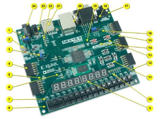
Figure 3.7:Artix 7 Nexys board
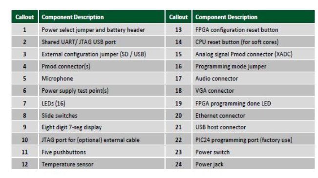
Table 3.1: Artix 7 board pin description
3.4.1 Power Supplies
The Nexys4 DDR board receives power from the Digilent USB-JTAG port (J6) or from an external power supply. Jumper JP3 (near power jack) determines which source is used to provide power supply.
All Nexys4 DDR power supplies can be turned on and off by using a single logic-level power switch (SW16). A power-good LED (LD22), driven by the “power good” output of the ADP2118 supply, indicates that the supplies are turned on and operated normally. An overview of the Nexys4 DDR power circuit is shown in Figure 3.8.
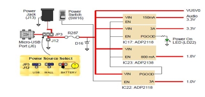
Figure 3.8 :Power circuit
The USB port can deliver sufficient power for the vast majority of designs. Our out-of-box demo draws ~400mA of current from the 5V input rail. A few applications require more power than the USB port can provide. Even some applications may need to run without being connected to a PC’s USB port.
In such cases, an external power supply or battery pack can be used. An external power supply can be used by plugging into the power jack (JP3) and setting jumper (J13) to “wall”. The supply should use a coax, center-positive 2.1mm internal-diameter plug and deliver 4.5VDC to 5.5VDC and 1A of current (i.e., at least 5W of power).
An external battery pack can be used by connecting the battery’s positive terminal to center pin of JP3 and the negative terminal to pin labeled J12, directly below JP3. Since the main regulator on the Nexys4 DDR cannot accommodate input voltages over 5.5VDC, an external battery pack must be limited to 5.5VDC. The minimum voltage of the battery pack depends on the application: if the USB Host function (J5) is used, at least 4.6V is needed. In other cases, the minimum voltage is 3.6V.
Voltage regulator circuits from Analog Devices create the required 3.3V, 1.8V, and 1.0V supplies from the main power input.
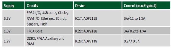
Table 3.2: Nexys board power supplies
3.4.2 Power Protection
The Nexys4 DDR features over current and over voltage protection on the input power rail. A 3.5A fuse (R287) and a 5V Zener diode (D16) provide a non-resettable protection for other on-board integrated circuits, as displayed in Figure 3.8. Applying power outside of the specs outlined in this document is not covered by warranty. If this happens, either or both might get damaged permanently. The damaged parts are not user-replaceable.
3.4.3 JTAG Configuration
The Xilinx instruments ordinarily speak with FPGAs utilizing the Test Access Port and Boundary-Scan Architecture, regularly alluded to as JTAG. Amid JTAG programming, a .bit record is exchanged from the PC to the FPGA board utilizing the locally available Digilent USB-JTAG hardware (port J6) or an outside JTAG software engineer, for example, the Digilent JTAG-HS2 which is joined to port J10. We can perform JTAG programming at whatever time after the Nexys4 DDR has been fueled on, paying little heed to sort of the mode jumper (JP1) is set to. On the off chance that the FPGA board is now designed, then the current setup is overwritten with the bitstream that is being transmitted over JTAG. By setting the mode jumper to JTAG setting, it can keep FPGA board from being arranged from some other bitstream source until a JTAG programming happens.
Programming the Nexys4 DDR with an uncompressed bitstream utilizing the on-board USB-JTAG hardware for the most part takes five seconds. JTAG writing computer programs is done utilizing the equipment server in Vivado or the iMPACT device included with ISE and the Lab Tools rendition of Vivado.
3.4.4 Memory
The Nexys4 DDR board contains two external memories. They are 1Gib (128MiB) DDR2 SDRAM and a 128Mib (16MiB) non-volatile serial Flash device. The DDR2 modules are integrated on-board and connected to the FPGA using the industry standard interface. A serial Flash will be on a dedicated quad-mode (x4) SPI bus.
3.4.5 DDR2
The Nexys4 DDR includes one Micron memory component, creating a single rank, 16- bit wide interface. It is routed to a 1.8V-powered High Range FPGA bank with 50 ohm controlled impedance. Its internal terminations in the FPGA are used to match the trace characteristics. Similarly, on-die terminations (ODT) are used for impedance matching on the memory side.
For appropriate operation of the memory, a memory controller and physical layer (PHY) interface should be incorporated into the FPGA plan. There are two prescribed approaches to accomplish that as examined underneath . They contrast both in multifaceted nature and plan adaptability.
The straight forward route is to utilize the Digilent-if DDR-to-SRAM connector module which instantiates the memory controller and utilizations a nonconcurrent SRAM transport for interfacing with client rationale. This module gives in reverse similarity than more established Nexys sheets including a CellularRAM rather than DDR2. It exchanges memory data transfer capacity for straightforwardness.
More propelled clients or the individuals who need to take in more about DDR SDRAM innovation need to utilize the Xilinx 7-arrangement memory interface arrangements center created by the MIG (Memory Interface Generator) Wizard. Contingent upon the device utilized (ISE, EDK or Vivado), the Wizard can create a local FIFO-style or an AXI4 interface to associate with client rationale. This work process permits the customization of a few DDR parameters enhanced for a specific application. Table 3.3 underneath records the MIG Wizard settings improved for the Nexys4 DDR.
Table : 3.3 : DDR2 settings for Nexys board
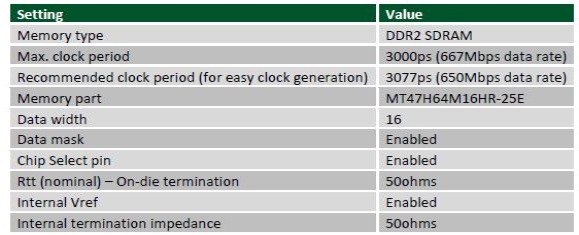
Although the FPGA, memory IC, and the board itself are capable of the maximum data rate of 667Mbps, the limitations in the clock generation primitives restrict the clock frequencies that can be generated from the 100 MHz system clock. Thus, for simplicity, the next highest data rate of 650Mbps is recommended.
3.4.6 Quad-SPI Flash
FPGA configuration files can be written to the Quad-SPI Flash and mode settings are available to cause the FPGA to automatically read a configuration from this device at power on. An Artix-7 100T configuration file requires less than four MiB (mebibyte) of memory, leaving about 77% of the flash device available for user data. Or, if the FPGA is getting configured from another source, the whole memory can be used for custom data.
The contents of the memory can be changed by issuing certain commands on the SPI bus. All signals in the SPI bus except SCK are general-purpose user Input Output pins after FPGA configuration. SCK is an exception because it remains as a dedicated pin even after the configuration. A special FPGA primitive called STARTUPE2 is used to provide an access to this pin.
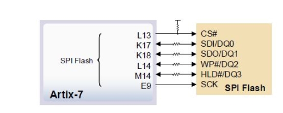
Figure 3.9 :Nexys DDR SPI Flash pinout
3.4.7 Oscillators/Clocks
The Nexys4 DDR board incorporates a solitary 100 MHz gem oscillator associated with stick (E3 is a MRCC contribution on bank 35). The info clock of FPGA can drive MMCMs or PLLs to create timekeepers of different frequencies and with known stage connections that might be required all through a plan.
Xilinx offers the Clocking Wizard IP center to help the clients to produce the distinctive tickers required for a particular plan. This will legitimately instantiate the required MMCMs and PLLs in view of the coveted frequencies and stage connections indicated by the client. The Wizard will then yield a simple to-utilize wrapper segment around these timing assets that can be embedded into the client’s outline. The timing wizard IP can be gotten to from inside the Project Navigator or Core Generator devices.
3.4.8 Basic I/O
The Nexys4 DDR board incorporates two tri-colour LEDs, sixteen slide switches, six push catches, sixteen individual LEDs, and an eight-digit seven-section show, as appeared in Figure 3.10. The pushbuttons and slide changes are associated with the FPGA through arrangement resistors to keep harm from incidental shortcircuits (a short out could happen if a FPGA stick appointed to a pushbutton or slide switch was coincidentally characterized as a yield). The five push catches are organized in an or more sign design called “flitting” switches that regularly produce a low yield when they are very still, and a high yield just when they are squeezed. The red pushbutton marked as “CPU RESET,” then again, creates a high yield when very still and a low yield when squeezed. The CPU RESET catch is planned to be utilized as a part of outlines to reset the processor, however we can likewise utilize it as a universally useful push catch. Slide switches creates consistent high or low sources of info relying upon their position.
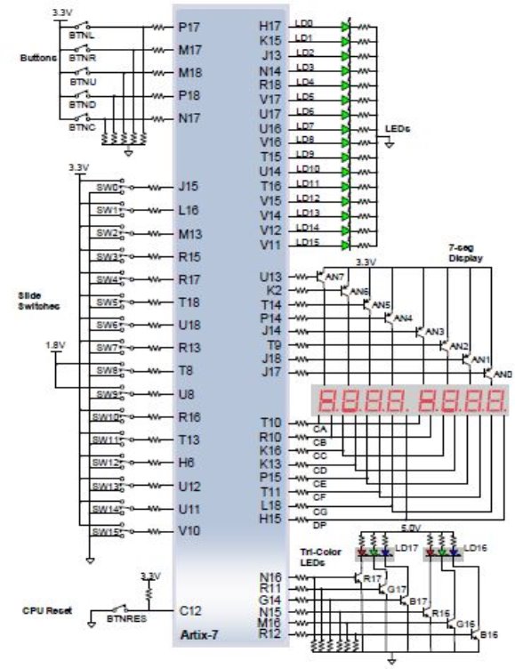
Figure 3.10: Basic I/o pin diagram
The sixteen high-efficiency LEDs are anode-connected to the FPGA via 330 ohm resistors. They will turn on when a logic high voltage is applied to their respective I/O pin. Additional LEDs that are not user-accessible indicate power-on, FPGA programming status, USB and Ethernet port status.
3.4.9 Seven – Segment Display
The Nexys4 DDR board contains two four-digit regular anode seven-portion LED show sections, arranged to act like a solitary eight-digit show. Each of the eight digits is made out of seven fragments masterminded in a “figure 3.10” example, with a LED installed in each section. Fragment LEDs can be lit up exclusively, so out of 128 examples, one example can be shown on a digit by lighting up certain LED portions and leaving the others dim, as appeared in Figure 3.11. Of these 128 conceivable examples, the ten relating to the decimal digits are the most valuable.
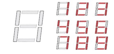
Figure 3.11 : Seven segment Display
The anodes of the seven LEDs shaping every digit are associated together into one “normal anode” circuit hub, yet the LED cathodes stay isolated, as appeared in Fig 3.12. The basic anode signs are accessible as eight “digit empower” input signs to the 8-digit show. The cathodes of same sections on every one of the 4 presentations are associated into seven circuit hubs named CA through CG. For instance, the eight “D” cathodes from the eight digits are gathered together into a solitary circuit hub called “Compact disc.” These seven cathode signs are accessible as contributions to the 8-digit show. A multiplexed show is made by utilizing this flag association, where the cathode signs are normal to all digits yet they can just enlighten the sections of the digit whose comparing anode flag is set. To light up a portion, the anode ought to be driven high while the cathode is driven low. Be that as it may, since the Nexys4 DDR utilizes transistors to drive enough current into the normal anode point, the anode empowers are altered. In this way, both the AN0..7 and the CA..G/DP signs are driven low when dynamic.
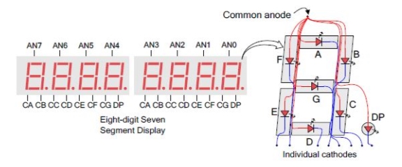
Figure 3.12 : Common anode association of seven segment display
This circuit drives the anode flags and comparing cathode examples of every digit in a rehashing, persistent progression at a refresh rate that is quicker than the human eye can recognize. Every digit is lit up for just a single eighth of the time, and eye can’t see the obscuring of a digit before it is lit up once more, the digit shows up constantly lit up. On the off chance that the refresh, or “revive”, rate is eased back to around 45Hz, a glint can be seen in the show.
For each of four digits to seem splendid and light up ceaselessly , every one of the eight digits ought to be driven once every 1 to 16ms, for a revive recurrence of around 1 KHz to 60Hz. For instance, in a 62.5Hz revive conspire, the whole show would be invigorated once every 16ms, and every digit would be lit up for 1/8 of the invigorate cycle, or 2ms. The controller ought to drive low the cathodes with the right example when the comparing anode flag is driven high. To outline the procedure, if AN0 is affirmed while CB and CC are declared, then a “1” will be shown in digit position 1. At that point, if AN1 is stated while CA, CB, and CC are attested, a “7” will be shown in digit position 2. In the event that AN0, CB, and CC are driven for 4ms, and after that AN1, CA, CB, and CC are driven for 4ms in a perpetual progression, the show will indicate “71” in the initial two digits. An illustration timing chart for a four-digit controller is appeared in Figure 3.13.
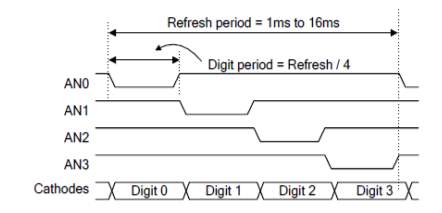
Figure 3.13 : Timing Diagram of seven segment display
3.5 Pin Configuration of Block Diagram with Respect to Artix-7 Boar
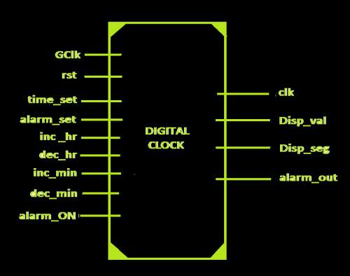
Figure 3.14 : Block Diagram
The block diagram gives in detail about the inputs and outputs of the Digital Clock.
INPUT PINS
1.GClk :It represents the global clock whose frequency is 100Mhz. In the program it is used to generate one second timing signal. This is given to pin E3 in Artix-7 FPGA board.
2. rst:Whenever rst is high all the values are set to zero. This is given to pin C12 in Artix-7 FPGA board.
3. time_set: This switch used to set the time in the clock. If the time_set switch is low then the clock runs asusual and if it is high new time has to be fed for the clock. This is given to pin J15 in Artix-7 FPGA board.
4.alarm_set : This switch used to set the alarm in the clock. If the alarm_set switch is low then the clock fixes the previous value in the alarm and if it is high new alarm time has to be fed for the clock. This is given to pin M13 in Artix-7 FPGA board.
5. inc_hr :This button is used to increment the hour value by one.This is given to pin N17 in Artix-7 FPGA board.
6. dec_hr :This button is used to decrement the hour value by one.This is given to pin M18 in Artix-7 FPGA board.
7. inc_min :This button is used to increment the hour value by one.This is given to pin P17 in Artix-7 FPGA board.
8. dec_min :This button is used to decrement the hour value by one.This is given to pin M17 in Artix-7 FPGA board.
9. Alarm_On :This switch is used to on and off the alarm. This is given to pin V10 in Artix-7 FPGA board.
OUTPUT PINS
1. Clk :This is derived from GClk. It is used to generate minute and hour signals. An LED is used to check the second signal. This is given to pin H17 in Artix-7 FPGA board.
2.Disp_seg :This is used to display numbers in the seven segment display . These values are given to pin no’s T10, R10, K16, K13, P15, Tll, L18 respectively in Artix-7 FPGA board.
3.Disp_Val : It is used to display numbers in the positions of seconds, minutes and hours. The 7-segment displays which are in use are highlighted and others are put low. These values are given to pin no’s J17, J18, T9, J14, P14, T14, K2, U13 respectively in Artix-7 FPGA board.
4. alarm_out: When clock time is equal to alarm time then the alarm_out signal becomes high otherwise remains in low position. When the alarm_out signal becomes high the LED to which this signal is interfaced glows. This is given to pin no V11 in Artix-7 FPGA board.
3.5.1 Purpose and Connectivity
1. C12 – It acts as a switch on nexys4 board. Whenever the switch is on, the system is reset otherwise the clock runs in normal mode.
2. J15 – It acts as a switch on nexys4 board. Whenever the switch is on, the clock time can be changed otherwise the clock runs with the previous set time.
3.M13 – It acts as a switch on nexys4 board. Whenever the switch is on, the alarm time can be changed otherwise the previous alarm time will be set.
4. N17 – It acts as a button on nexys4 board. When the button is pressed the hour value gets incremented by one.
5. M18 – It acts as a button on nexys4 board. When the button is pressed the hour value gets decremented by one.
6.P17 – It acts as a button on nexys4 board. When the button is pressed the minute value gets incremented by one.
7. M17 – It acts as a button on nexys4 board. When the button is pressed the minute value gets decremented by one.
8. V10 – It acts as a switch on nexys4 board. When the switch is on, the alarm is on otherwise the alarm is in off state.
9. H17 – It is a LED on nexys4 board. When the second signal is generated this LED glows indicating one second.
10. T10, R10, K16, K13, P15, T11, L18 – These pins are connected to the LED’s in the seven segment display.
11. T9 – This pin is used to display MS bit of hour using 7 segment display.
12. J14 – This pin is used to display LS bit of hour using 7 segment display.
13. P14 – This pin is used to display MS bit of minute using 7 segment display.
14. T14 – This pin is used to display LS bit of minute using 7 segment display.
15. K2 – This pin is used to display MS bit of second using 7 segment display.
16. U13 – This pin is used to display LS bit of second using 7 segment display.
17. V11 – This is a LED in nexys4 board which glows when the clock time is same as the alarm time.
3.5.2 Scalar and Vector I/O pins
Scalar I/O pins consists of only scalar values either 0 or 1.
Scalar Input pins
- GClk
- rst
- time_set
- alarm_set
- inc_hr
- dec_hr
- inc_min
- dec_min
- alarm_ON
Scalar Output pins
- clk
- alarm_out
Vector I/O pins consists of vector values more than one stored in them.
Vector Output pins
- Disp_val
- Disp_seg
CHAPTER 4: Software Design and Implementation of Digital Clock
4.1 Description and Features of Vivado
4.1.1 Description of Vivado
The Vivado Design Suite is intended to enhance efficiency. This totally new instrument suite is architected to expand the general efficiency for outlining, coordinating, and executing with the Xilinx 7 arrangement, Zynq-7000 All Programmable, and Ultra Scale gadgets. With the Vivado Design Suite, you can quicken outline usage with place and course apparatuses that logically streamline for numerous and simultaneous plan measurements, for example, timing, clog, add up to wire length, use and power. Based on the common adaptable information model of the Vivado Design Suite, the whole outline process can be executed in memory without writing or interpret any moderate document positions, which quickens runtimes, troubleshoot, and usage while lessening memory necessities. The Vivado Design Suite gives you plan investigation capacities at each outline organize. This takes into consideration outline and device setting alterations prior in the plan forms where they have less general timetable effect, hence decreasing plan emphasess and quickening efficiency. There are diverse strides to be performed in Vivado configuration apparatus.
Steps to be followed in Vivado:
The first step is to open the Vivado design tool .Click on the Vivado 2016.2 icon. After clicking, the following window pops up. The windows has different options like open a project, create new project, open example project etc.
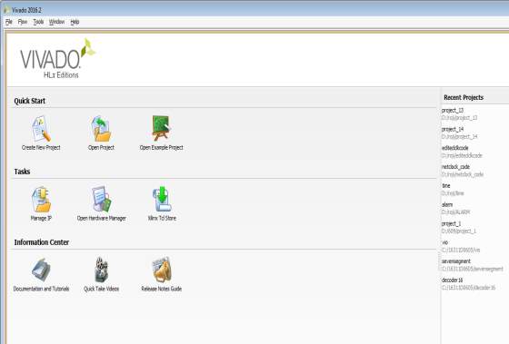
Figure 4.1 : Open or create project in Vivado
In this window, select Create New Project after which a small window named New Project appears as shown below.
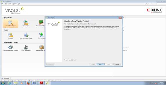
Figure 4.2 : creating a project
Now the New Project window prompts for Project Name and Project Location.
Specify the desired Project Name and Project Location and click on Next.
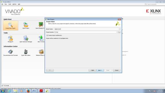
Figure 4.3 : Selecting the project path and project name
Select the RTL Project radio button and click on Next.
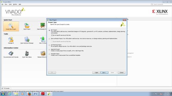
Figure 4.4 : Selecting the project type
Here click on do not specify sources at the time. This means that the sources files cannot be added at the time of project creation.
In the next dialogue box, Default Part Product Category, Family, Package, Speed Grade, Temperature Grade of the board should be specified as follows:
Product Category: All
Speed Grade: -1
Family :Artix-7
Package :cgs324
Temp Grade : C
Next we have to select Artix series xc7a100tcsg324-1 and click on Next.
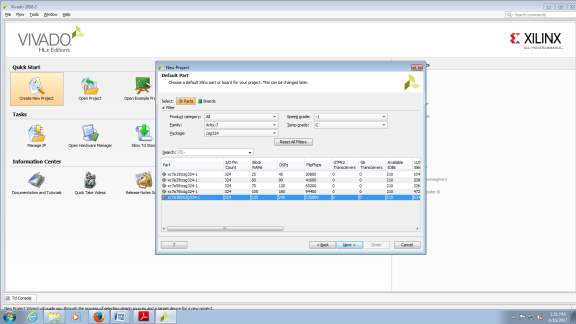
Figure 4.5 : Selecting the Specifications
Next our Project Summary will be displayed in which we have to check if our project specifications are met and click on Finish.
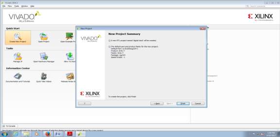
Figure 4.6 : Displaying the Project Summary
In the Project Manager window, click on add sources and the following window appears in which we have to select Add or create design sources and click on next.
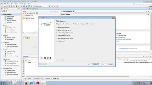
Figure 4.7 : Adding or Creating the files
Click on Create file and give a file name and click on Finish.
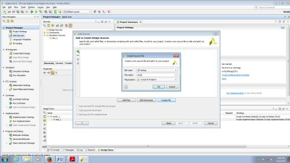
Figure 4.8 : Creating a file and giving file name
A file will be created in which we have to write our code.
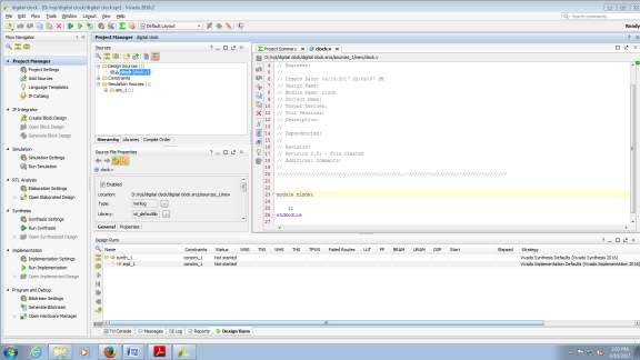
Figure 4.9 :Writing the code in the file created
After writing our code in the window, click on Run Simulation.
When the code is simulated correctly, go for synthesis and implementation.Before synthesis, create an XDC(Xilinx Design Constraint) file for mapping of input output pins on the board. After synthesized successfully, click on run implementation. When the code gets implemented, we can generate bit stream.
For generating Bitstream, click on Generate Bitstream.When the Bitstream is generated successfully, we can connect our FPGA board to the system via a cable to dump the code in the kit.After dumping the code into the kit we can verify the output on the board.
4.1.2 Features of Vivado
1. Fit more into a device, faster.
2. Vivado delivers robust performance and low power with predictable results.
3. Vivado Design Suite delivers unparalleled runtime and memory utilization.
4. C-based IP Generation with Vivado High-Level Synthesis.
5. Model-based DSP design integration using System Generator for DSP.
6. Block-based IP integration with Vivado IP Integrator.
7. Vivado Integrated Design Environment for Design and Simulation.
8. Comprehensive hardware debug.
9. Accelerate Verification by >100X with C, C++, and SystemC.
4.2 Description and features of Verilog HDL
4.2.1 Description of Verilog
Verilog HDL is a hardware description language used to design and document electronic systems. Verilog HDL allows designers to design at various levels of abstraction. It is the most widely used HDL with a user community of more than 50,000 active designers.
Hardware Description Language
Have high-level language constructs to describe the functionality and connectivity of the circuit.
Can describe a design at some levels of abstraction – Behavioral, RTL, Gate-level, Switch.
Can describe functionality as well as timing.
Can be used to model the concurrent actions in real hardware.
Can be used to document the complete system design tasks – testing, simulation … related activities.
Comprehensive and easy to learn.
Verilog HDL
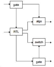
Figure 4.10 : Verilog design flow
- Hardware description language
- Mixed level modelling
– Behavioral
Algorithmic
Register transfer
– Structural
Gate
Switch
- Single language for design and simulation
- Built-in primitives and logic functions
- User-defined primitives
- Built-in data types
- High-level programming constructs
Verilog models can be developed for different levels of abstraction. These levels of abstraction and their corresponding model types are as follows:
Algorithmic a model that implements a design algorithm in high-level language constructs.
RTL a model that describes the flow of data between registers and how a design processes that data.
Gate-level a model that describes the logic gates and the connections between logic gates in a design.
Switch-level a model that describes the transistors and storage nodes in a device and the connections between them.
The basic building block of the Verilog HDL is the module. The module format facilitates top-down and bottom-up design. A module contains a model of a design or part of a design. Modules can incorporate other modules to establish a model hierarchy that describes how parts of a design are incorporated in an entire design. The constructs of the Verilog HDL, such and its declarations and statements, are enclosed in modules.
The Verilog HDL behavioral language is structured and procedural like the C programming language. The behavioral language constructs are for algorithmic and RTL models. The behavioral language provides the following capabilities:
- structured procedures for sequential or concurrent execution
- explicit control of the time of procedure activation specified by both delay expressions and by value changes called event expressions
- explicitly named events to trigger the enabling and disabling of actions in other procedures
- procedural constructs for conditional, if-else, case, and looping operations
- procedures called tasks that can have parameters and non-zero time duration
- procedures called functions that allow the definition of new operators
- arithmetic, logical, bit-wise, and reduction operators for expressions
The Verilog HDL structural language constructs are for gate-level and switch-level models. The structural language provides the following capabilities:
- a complete set of combinational primitives
- primitives for bidirectional pass and resistive devices
- the ability to model dynamic MOS models with charge sharing and charge decay.
Verilog structural language models can accurately model signal contention. In the Verilog HDL, structural modeling accuracy is enhanced by primitive delay and output strength specification. Signal values can have different strengths and a full range of ambiguous values to reduce the pessimism of unknown conditions.
4.2.2 Features of Verilog HDL
- set break points during simulation that stop the simulation and allow you to enter an interactive mode to examine and debug your design.
- display information about the current state of the design and to specify the format of that information.
- apply stimulus during simulation.
- circuit patching during simulation.
- tracing the execution flow of the statements in your model.
- traversing the model hierarchy to various regions of your design to examine the state of the simulation in that region.
- stepping through the statements of a design and executing them one at a time.
- displaying the active statements in a design.
- displaying and disabling the operations you entered in interactive mode.
- reading data from a file and writing data to that file.
- saving the current state of a simulation in a file and restoring that simulation at another time.
- investigating the performance ramifications of architectural decision—stochastic modeling.
4.3 Project Design Flow Steps
Flowchart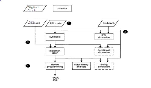
Figure 4.11 Project Design Flow
Description of the inputs and outputs of the digital clock
- Gclk :- On board clock with frequency 100Mhz.
- Time_set :- It is used to set the time in the clock.
- Alarm_set :- It is used to set the alarm in the clock.
- Inc_hr :- It increments the hour by one value.
- Inc_min :- It increments minute by one value.
- Dec_hr :- It decrements hour by one value.
- Dec_min :- It decrements minute by one value.
- Rst :- Initializes all the vales to zero.
- Alarm_ON :- It is used to switch on the alarm.
- Alarm_out :- Displays the alarm value.
- Disp_Val :- Displays the time value.
- Disp_Seg :- Initiates the segment in which the value is displayed.
- Clk :- Displays every second.
4.3.1 Clock Generation for 1 Second
Flowchart
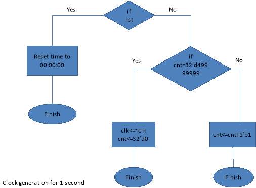
Figure 4.12 : Flow chart for generation of one second
One second signal is generated initially from the global clock.
if(rst) //rst used to RESET time to 00:00:00
clk
else if(cnt == 32’d49999999)
begin
clk
cnt
end
else
cnt
4.3.2 Alarm Time Set
Flowchart
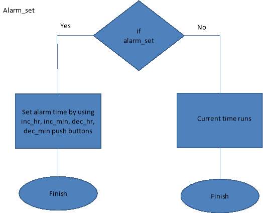
Figure 4.13 : Flow chart for alarm time set
Procedure to set the alarm time.
A. For incrementing hour :
if(inc_hr==1’b1)//If inc_hr push button (M18) is pressed
begin
if(outh==6’d24)
alarmh
else
alarmh
end
Explanation: If the inc_hr push button is high i.e., equal to one then the value of the hour
gets incremented , if hour value is 24 then the value gets assigned to zero.
B. For incrementing minute :
if(inc_min==1’b1)// If inc_min push button (P17) is pressed
begin
if(outm==6’d60)
alarmm
else
alarmm
end
Explanation: If the inc_min push button is high i.e., equal to one then the value of minute
gets incremented , if minute value is 60 then the value gets assigned to zero.
C. For decrementing hour:
if(dec_hr==1’b1)// If dec_hr push button (M17)is pressed
begin
if(outh==6’d24)
alarmh
else
alarmh
end
Explanation: If the dec_hr push button is high i.e., equal to one then the value of the hour
gets decremented , if hour value is 24 then the value gets assigned to zero.
D. For decrementing minute :
if(dec_min==1’b1)// If dec_min push button (P18)is pressed
begin
if(outm==6’d60)
alarmm
else
alarmm
end
Explanation: If the dec_min push button is high i.e., equal to one then the value of minute
gets decremented , if minute value is 60 then the value gets assigned to zero.
4.3.3 Current Time Set
Flowchart
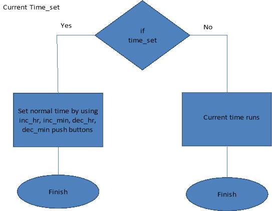
Figure 4.14 : Flow chart for current time set
Procedure to set the current time.
A. For incrementing hour :
if(inc_hr==1’b1)// If inc_hr push button (M18) is pressed
begin
if(outh==6’d24)
outh
else
outh
end
Explanation: If the inc_hr push button is high i.e., equal to one then the value of the hour
gets incremented , if hour value is 24 then the value gets assigned to zero.
B. For incrementing minute :
if(inc_min==1’b1) // If inc_min push button (P17) is pressed
begin
if(outm==6’d60)
outm
else
outm
end
Explanation: If the inc_min push button is high i.e., equal to one then the value of minute
gets incremented , if minute value is 60 then the value gets assigned to zero.
C. For decrementing hour :
if(dec_hr==1’b1)// If dec_hr push button (M17)is pressed
begin
if(outh==6’d24)
outh
else
outh
end
Explanation: If the dec_hr push button is high i.e., equal to one then the value of the hour
gets decremented , if hour value is 24 then the value gets assigned to zero.
D. For decrementing minute :
if(dec_min==1’b1)// If dec_min push button (P18)is pressed
begin
if(outm==6’d60)
outm
else
outm
end
Explanation: If the dec_min push button is high i.e., equal to one then the value of minute
gets decremented , if minute value is 60 then the value gets assigned to zero.
4.3.4 Real Time
Flowchart
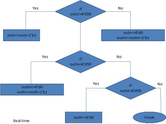
Figure 4.15 Flow chart for real time
Procedure to make the clock run usually.
if(outs!=6’d59)
outs
else
begin
outs
outm
end
if(outm==6’d59)
begin
outm
outh
end
if(outh==6’d24)
outh
end
Explanation: If the outs is not equal to 59 then the seconds value gets incremented and if it equal then the second is made to 00 and the minute value is incremented .Both the minute and seconds work simultaneously according to the conditions .when the conditions like hour is 24,minute is 60,second is 59 then the values will be set to 00.This function like normal real timeclock.
Alarm On
Flowchart
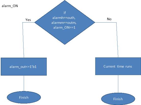
Figure 4.16 : Flow chart for alarm on
The condition for the alarm to get to high state.
always @ (*)
begin
alarm_out
if ((alarmh == outh) && (alarmm == outm) && (alarm_ON == 1))
alarm_out
end
Explanation: When both alarm values and current values are equal and if alarm button is on then the alarm is produced and it is indicated by using and led blink which blinks for one minute.
Displaying Values in Each Segment
Procedure to display values in individual segment.
if(rst)
begin
Disp_Val
Disp_Seg
end
if(CntRec == 16’d10922)
begin
if(!alarm_set) begin
Disp_Val
Disp_Seg
else begin
Disp_Val
Disp_Seg
end
if(CntRec == 16’d21844)
begin
if(!alarm_set) begin
Disp_Val
Disp_Seg
else begin
Disp_Val
Disp_Seg
end
if(CntRec == 16’d32766)
begin
if(!alarm_set) begin
Disp_Val
Disp_Seg
else begin
Disp_Val
Disp_Seg
end
if(CntRec == 16’d43688)
begin
if(!alarm_set) begin
Disp_Val
Disp_Seg
else begin
Disp_Val
Disp_Seg
end
if(CntRec == 16’d54610)
begin
if(!alarm_set) begin
Disp_Val
Disp_Seg
else begin
Disp_Val
Disp_Seg
end
if(CntRec == 16’d65532)
begin
if(!alarm_set) begin
Disp_Val
Disp_Seg
else begin
Disp_Val
Disp_Seg
End
Explanation: There are total eight segments on seven segment display of ARTIX 7 FPGA board. Each two segments are assigned to display seconds, minutes, hours accordingly. The display of digit on the segment is done by 7 segment led interfacing and its value is displayed to according to value assigned to Disp_Val. Total there 12 sets of value out of them 6 are for current values and other for alarm values. The value is displayed on the particular segment assigned by using the binary representation to Disp_Seg.
Seven – Segment Display
Procedure to display number on seven segment display
input [3:0] bcd;
output [7:0] outseg;
case(bcd)
5’h00: outseg
5’h01: outseg
5’h02: outseg
5’h03: outseg
5’h04: outseg
5’h05: outseg
5’h06: outseg
5’h07: outseg
5’h08: outseg
5’h09: outseg
default :outseg
endcase
Explanation:The digit is displayed by using seven segment LED interfacing. In this each led segment is active low (led glows for 0 ).Each segment is represented by using their corresponding alphabet as abcdefg and the dp(decimal) point is represented by h. According to the digit, the alphabet segment glows and is represented as in the above process.
Taking the Input values
Procedure to take the input values required for the clock.
input [5:0] bin;
output [3:0] bcd1;
output [3:0] bcd0;
case (bin)
6’d0 : begin bcd1
6’d1 : begin bcd1
6’d2 : begin bcd1
6’d3 : begin bcd1
6’d4 : begin bcd1
6’d5 : begin bcd1
6’d6 : begin bcd1
6’d7 : begin bcd1
6’d8 : begin bcd1
6’d9 : begin bcd1
6’d10 : begin bcd1
6’d11 : begin bcd1
6’d12 : begin bcd1
6’d13 : begin bcd1
6’d14 : begin bcd1
6’d15 : begin bcd1
6’d16 : begin bcd1
6’d17 : begin bcd1
6’d18 : begin bcd1
6’d19 : begin bcd1
6’d20 : begin bcd1
6’d21 : begin bcd1
6’d22 : begin bcd1
6’d23 : begin bcd1
6’d24 : begin bcd1
6’d25 : begin bcd1
6’d26 : begin bcd1
6’d27 : begin bcd1
6’d28 : begin bcd1
6’d29 : begin bcd1
6’d30 : begin bcd1
6’d31 : begin bcd1
6’d32 : begin bcd1
6’d33 : begin bcd1
6’d34 : begin bcd1
6’d35 : begin bcd1
6’d36 : begin bcd1
6’d37 : begin bcd1
6’d38 : begin bcd1
6’d39 : begin bcd1
6’d40 : begin bcd1
6’d41 : begin bcd1
6’d42 : begin bcd1
6’d43 : begin bcd1
6’d44 : begin bcd1
6’d45 : begin bcd1
6’d46 : begin bcd1
6’d47 : begin bcd1
6’d48 : begin bcd1
6’d49 : begin bcd1
6’d50 : begin bcd1
6’d51 : begin bcd1
6’d52 : begin bcd1
6’d53 : begin bcd1
6’d54 : begin bcd1
6’d55 : begin bcd1
6’d56 : begin bcd1
6’d57 : begin bcd1
6’d58 : begin bcd1
6’d59 : begin bcd1
6’d60 : begin bcd1
default:begin bcd1
endcase
Explanation: The input values taken are incremented accordingly and stored in output segments.
CHAPTER – 5 Results and Discussion
The proposed Digital clock design displays the time on seven segment display of FPGA board. The functional blocks are designed by using Verilog Hardware Description language. As discussed earlier initially a second clock is generated by using global clock and according to that clock , the second pulse gets incremented and when it is equal to 59 then it is set to zero and minute pulse is incremented and similarly the hour pulse will incremented when it is 60 minutes. The time can be set by using inc_hr ,inc min, dec_hr, dec_min push buttons. When time_set is on we can set the current time and when alarm set is on, the alarm time is set. Alarm_on button is provide to make alarm on and off. All these operations are displayed on the board and verified. These can be performed by using various steps :
5.1 Synthesis
- Click on add constrains and create axdc file.
- xdc file contains the hardware pin configuration of nexys4 board of FPGA
(Field Programmable Gate Array).
- In the xdc file the interfacing of the digital clock to hardware is done.
In the xdcfile , the mapping of the input-ouput pins takes place with respect to FPGA board.
The different pins mapped are C12-global clock, J15- time-set,M13-Alarm _set,N17-inc_hr,M18-dec_hr,P17-inc_min,M17- dec_min,V10- alarm_on,H17-second clock,V11-alarm out and seven segment pins for displaying the output.
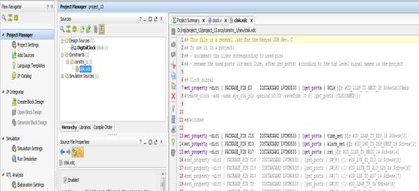
Figure 5.1 : XDC design file
After the creation of xdc file save the file and click on run synthesis option which lies in the toolbar left side of the screen.
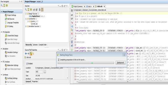
Figure 5.2 : Running Synthesis
- If there are any errors reopen the file and rectify them.
- If the file is synthesized successfully, then it has to be implemented.
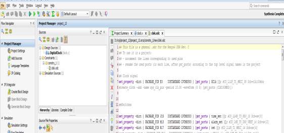
Figure 5.3 : Synthesis completed successfully
The successful completion of synthesis indicates that each and every pin is mapped correctly.
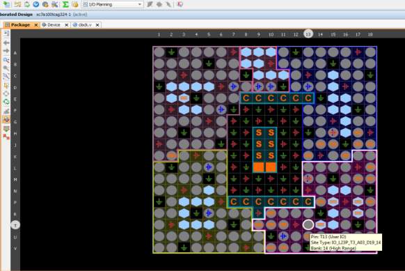
Figure 5.4 : Elaborated design
From the Elaborated design we can verify the pins that are assigned by clicking on the design. There are both horizontal rows and vertical columns named with alphabets and numbers respectively.
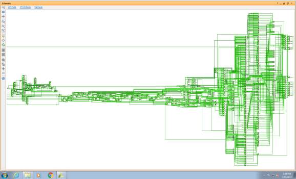
Figure 5.5: Synthesis schematic
5.2 Implementation
- Click on run implementation file in the tool box left on the screen.
- After the successful implementation of the file there will a dialogue box appearing on the screen.
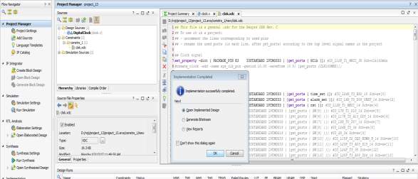
Figure 5.6: Implementation completed successfully
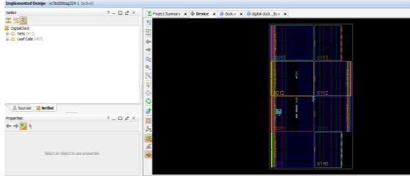
Figure 5.7: Implementation Design
In the implemented design , there are total 511 nets and 457 leaf cells.
5.3 Bit stream Generation
- After the file is implemented successfully then a bit stream file has to be generated which interfaces the file with hardware nexys4 board.
- When the dialogue box appears on the screen click generate bit stream option.
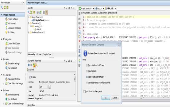
Figure 5.8 : Bit stream is generated
- This generates a bit stream file of the program.
- If there are any errors in interfacing, then the bit stream file will not be generated and the errors are to be corrected in the xdc file.
- If the bit stream is successfully generated, it results in successful hardware interface.
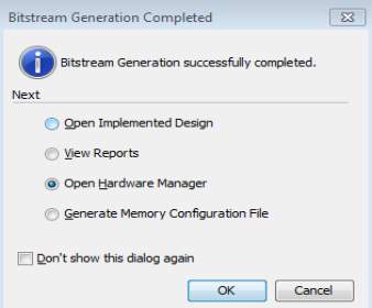
Figure 5.9 : Connection of hardware
- Now, click on the option open hardware manager and select the target.
- Then click on program option in the displayed dialogue box.
- This results in hardware implementation of digital clock
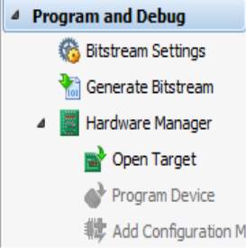
Figure 5.10 : Programming the device
5.4 Digital clock Output
Current Time
As discussed earlier the current time is set by using time set assigned to J15(switch 1) and inc_hr ,inc_min, dec_min,dec_hr assigned to push buttons N17,P17,M17,M18 respectively. As shown in the figure the current time is set at 02:09:54.
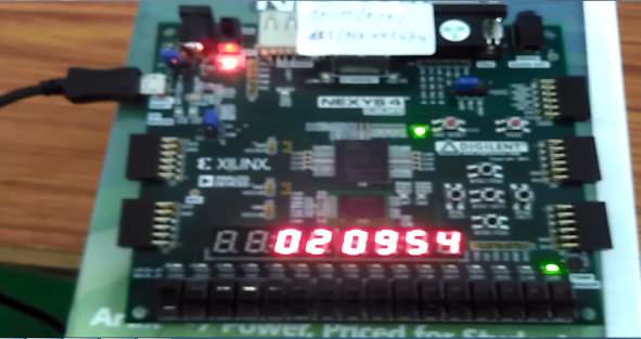
Figure 5.11: Displaying the current time
Alarm time
As discussed earlier the alarm time is set by using alarm set assigned to M13(switch 3) and inc_hr ,inc_min, dec_min,dec_hr assigned to push buttons N17,P17,M17,M18 respectively. As shown in the figure the alarm time is set at 02:10:00.
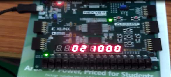
Figure 5.12 :Displaying the Alarm time
5.5 Power Report
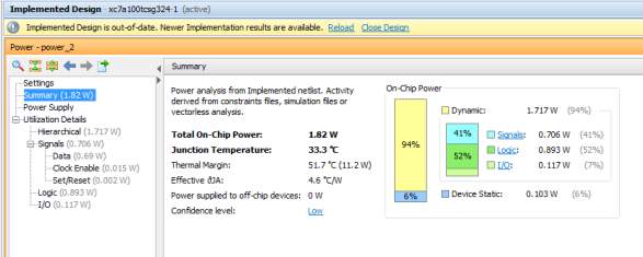
Figure 5.13 : Power Utilisation
The power utilisation describes about the percentage of the power used by the code of the digital clock. From the above figure it is clear that the power used by the logic is more than the signals.
5.6 Noise Report
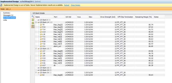
Figure 5.14 : Noise Report
The noise report gives the detailed description of the noise of each and every pins of the digital clock assigned on the FPGA board.
5.7 Utilization Report
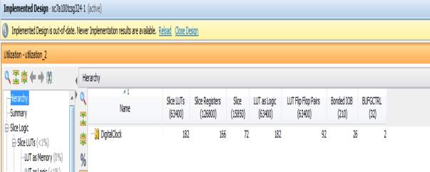
Figure 5.15 :Utilisation Report
The utilisation Report gives the details about the utilisation of number of slice registers , LUT as logic, LUT as flipflops ,slices etc. The utilisation is indicated in numbers or percentage.
5.8 Timing Analysis
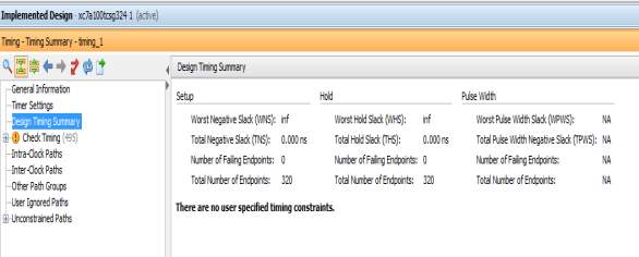
Figure 5.16 : Timing analysis Report
The Timing analysis report indicates the time consumed by the digital clock design code.
5.9 Summary Report
The Summary Report gives the overall synopsis of the project. It gives the information about the name of the project, project part, product family, module name, type of HDL etc., .It also gives overall view of the status of synthesis and implementation report with the number of warnings. It also states about the timing , power and utilisation .
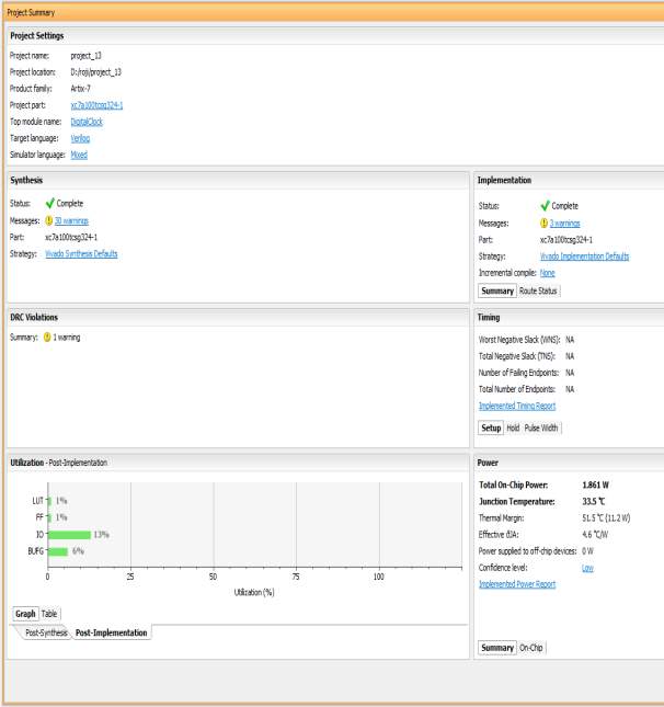
Figure 5.17: Summary Report
Conclusion
The high performance digital clock design is proposed with reduced core area. The block diagram of clock is designed with the combination of comparator, counter.The simple blocks incorporated with the clock reduced the area of the design appropriately. The performance of the clock is improved with highly adoptable clocking technique. The blocks are implemented using Verilog HDL and verified in the Vivado. The HDL program is also synthesized to obtain the logic blocks and sub-blocks of digital clock. The demonstration of digital clock is performed with the Artix 7 FPGA Evaluation Kit.
Future scope
The implementation of digital clock uses all the digits of the seven-segment display and is fully functional. It has 24 hour format and we can change the 24 hour to 12 hour A.M./P.M.format.We can enhance this project to display (dd/mm/yy).We can make the alarm more than once.
References
1. Ahmed MA, Rani DE, Sattar SA. FPGA based high speed memory BIST controller for embedded applications. Indian Journal of Science and Technology. 2015 Dec; 8(3):1–8. DOI: 10.17485/ijst/2015/v8i33/76080.
2. Kumar MS, Inthiyaz S, Mounica J, Bhavani M, Adidela CN, Endreddy B. FPGA implementation by using XBee Transceiver. Indian Journal of Science and Technology. 2016 May; 9(1):1–6. DOI: 10.17485/ijst/2016/v9i17/93032.
3. Navamani JD, Vijayakumar K, Lavanya A. FPGA-based digitally controlled Isolated Full-Bridge DC-DC Converter with Voltage Doubler (IFBVD). Indian Journal of Science and Technology. 2016 Apr; 9(16):1–7. DOI: 10.17485/ijst/2016/v9i16/76672.
4. Huda S, Anderson J, Tamura H. Optimizing effective interconnect capacitance for FPGA power reduction. Proceedings of the 2014 ACM/SIGDA International Symposium on Field-programmable Gate Arrays, ACM; 2014.
5. Kumar T, Das T, Pandey B, Rahman A, Kaur A, Hussain DMA. LVTTL based energy efficient watermark generator design and implementation on FPGA, IEEE International Conference on ICT Convergence, Busan: Korea; 2014 Oct 22–24.
6. Bansal M, Bansal N, Saini R, Pandey B, Kalra L, Hussain D. SSTL I/O standard based environment friendly energy efficient ROM design on FPGA. 3rd International Symposium on Environment-friendly Energies and Applications (EFEA’2014), Paris: France; Nov 19–21.
7. Kumar T, Das T, Pandey B, Hussain DMA. IO standard based thermal/energy efficient green communication for wi-fi protected access on FPGA. 6th IEEE International Congress on Ultra-Modern Telecommunications and Control systems and Workshops, St. Petersburg: Russia; 2014 Oct 06–08.
8. BDTI, “An Independent Evaluation of: The AutoESLAutoPilo High-Level Synthesis Tool,”2010.[Online].Available:http://www.bdti.com/Resources/BenchmarkResults/HLSTCP/AutoPilot
9. A. Canis, J. Choi, M. Aldham, V. Zhang, A. Kammoona, J. H. Anderson,S. Brown, and T.Czajkowski, “LegUp: High-LevelSynthesis for FPGABased Processor/Accelerator Systems,” in Proc. 19th ACM/SIGDA Int. Symp.on Field Programmable Gate Arrays, 2011, pp. 33–36.
10. J. Villarreal, A. Park, W. Najjar, and R. Halstead, “Designing Modular Hardware Accelerators in C with ROCCC 2.0,” in Proc. Symp.on Field- Programmable Custom Comput. Mach., 2010, pp. 127–134.
11. W. Meeus, K. Van Beeck, T. Goedem´e, J. Meel, and D. Stroobandt, “An Overview of Todays High-Level Synthesis Tools,” Design Automation for Embedded Systems, pp. 1 – 21, Aug. 2012.
12. S. Sarkar, S. Dabral, P. Tiwari, and R. Mitra, “Lessons and Experiences with High-Level Synthesis,” IEEE Des. Test. Comput., vol. 26, no. 4, pp. 34–45, Jul. 2009.
13. T. Kanungo, D. Mount, N. Netanyahu, C. Piatko, R. Silverman, and A. Wu, “An Efficient K-Means Clustering Algorithm: Analysis and Implementation,” IEEE Trans. Pattern Anal. Mach. Intell., vol. 24, no. 7, pp. 881–892, Jul. 2002.
14. F. Winterstein, S. Bayliss, and G. Constantinides, “FPGA-Based K Means Clustering using Tree-Based Data Structures,” in Proc. Int. Conf.on Field Programmable Logic and Appl., 2013, pp. 1–6.
15. Kaltoth, REQUIREMENT FOR THE PERSONA CONCEPT, 2nd international workshop on requirements engineering for high assurance systems (rhas 03), September 9,2003. monterery bay, California. USA. inconjection with IEEE international requirements engineering conference.
16. David Lee, MihalisYannakakis, Principles and Methods of Testing Finite State Machines, AT&T Bell Laboratories, Murray Hill, New Jersey.
17. Amr T. Abdel-Hamid, Mohamed Zaki and SofieneTahar, A Tool Converting Finite State Machine to VHDL, published in IEEE 2004.
18. Abhilasha Sharma and KavitaSaroch, FPGA Based System Login Security Lock Design using Finite State Machine, IOSR Journal of Electronics and Communications.
19. https://www.google.co.in/?gfe_rd=ctrl&ei=jVYfU7DKGMKW8Qe4iIGgDw&gws_rd=cr#q=Programmable+Logic+and+Application+Specific+Integrated+Circuits
20. Sergei Devadze, MargusKruus, Alexander Sudnitson, Web-Based Software Implementation of Finite State Machine Decomposition for Design and Education, CompSysTech’2001 – Bulgarian Computer Science Conference – 21-22.06.2001, Sofia, Bulgaria.
21. Iuliana CHIUCHISAN, Alin Dan POTORAC, Adrian GRAUR “Stefancel Mare”, Finite State Machine Design and VHDL Coding Techniques, 10th International Conference on Development and Applications Systems, Suceava, Romania, May 27-29, 2010.
22. M. Rebaudengo, M. SonzaReorda, M. ViolantePolitecnico di Torino, A new functional fault model for FPGA Application-Oriented testing.
23. StaveTrimberger, Dean Caeberry, Anders Johnson, Jennifer Wong, A Time – Multiplexed FPGA, IEEE 1997.
24. DORON DRUSINSKY AND DAVID HAREL, Using Statecharts for Hardware Description and Synthesis, IEEE TRANSACTIONS ON COMPUTER-AIDED DESIGN.VOL.8.NO.7.JULY1989.
25. PrabhatRanjan , DR. Kulbir Singh, Implementation of FIR Filters on FPGA.
26. https://www.google.co.in/?gfe_rd=ctrl&ei=jVYfU7DKGMKW8Qe4iIGgDw&gws_rd=cr#q=High- Level+Synthesis+Tools+for+Xilinx+FPGAs.
27. MichealGschwind, Valentina Salapura, Optimizing VHDL code for FPGA targets.
28. Dave Landis, Ph.D., P.E., Programmable Logic and Application Specific Integrated Circuits
29. Sergei Devadze, MargusKruus, Alexander Sudnitson, Web-Based Software Implementation of Finite State Machine Decomposition for Design and Education, CompSysTech’2001 – Bulgarian Computer Science Conference – 21-22.06.2001, Sofia, Bulgaria.
30. IEEE Standards Association: IEEE Standard 1685-2009, IEEE Standard for IP-XACT,Standard Structure for Packaging, Integrating, and Reusing IP within Tool Flows http://standards.ieee.org/findstds/standard/1685-2009.html
31. Berkeley Design Technology, Inc.: An Independent Evaluation of High-Level SynthesisToolsforXilinxFPGAshttp://www.xilinx.com/technology/dsp/BDTI_techpaper.pdf
32. http://www.xilinx.com/warranty.htm#critapps.
33. Vivado® Design Suite User Guide: Release Notes, Installation, and Licensing (UG973)
34. ISE® Design Suite 14: Release Notes, Installation, and Licensing (UG631)
35. Vivado Design Suite User Guide: Using the Vivado IDE (UG893)
36. Vivado Design Suite User Guide: Design Analysis and Closure Techniques (UG906)
37. ISE to Vivado Design Suite Migration Guide (UG911)
38. Vivado Design Suite User Guide: Using Constraints (UG903)
Cite This Work
To export a reference to this article please select a referencing stye below:
Related Services
View all


Related Content
All TagsContent relating to: "Computer Science"
Computer science is the study of computer systems, computing technologies, data, data structures and algorithms. Computer science provides essential skills and knowledge for a wide range of computing and computer-related professions.
Related Articles

DMCA / Removal Request
If you are the original writer of this dissertation and no longer wish to have your work published on the UKDiss.com website then please: