Smart Trolley System for Automated Billing Using RFID
Info: 14682 words (59 pages) Dissertation
Published: 3rd Sep 2021
Tagged: Information Systems
ABSTRACT
Now a days interest in shopping malls is widely increasing among people. People get daily necessities from shopping malls. There is an emerging demand for easy and quick payment of bills in shopping malls. Shoppers are frustrated at locating the items on the shopping list when shopping in shopping malls and when no assistance is available in shopping. To eliminate these problems, each product in the shopping mall will be provided with a RFID tag, to identify its type. Each shopping cart is implemented with a Product Identification Device (PID) that contains a microcontroller, an LCD, RFID reader and a ZIGBEE transmitter. RFID reader will read the purchasing product information on the shopping cart and the information about the product is displayed on LCD which is interfaced to the microcontroller. At the billing counter, the total bill will be transferred to PC at the counter side by using ZIGBEE module.
In this project, AT89S52 microcontroller is attached to an RFID reader and a barcode reader. As the user puts items in the trolley the reader on the trolley reads the tag and sends a signal to the controller. The controller then stores it in the memory and compares it with product ID. If it matches, it shows the name of item on LCD and also total amount of items purchased. Once the shopping is finished, the customer will press a button on the trolley send the total amount spent on the products to the billing counter section using ZIGBEE wireless communication module. In this project, there is a chance to revert back the product according to our need and budget. Once you take back product from the trolley, the same card will be again read by the RFID reader, then the controller will deduct the same amount associated to that product, from the net bill amount. The bill amount will be received by the ZIGBEE receiver and sent to the PC to display in the Hyper Terminal.
CONTENTS
Acknowledgement iv
Abstract v
List of Figures vi
List of tables vi
Introduction
Page No.
1.1 Introduction 1
1.2 Existing System 1
1.3 Proposed System 2
1.4 Scope of Study 2
Literature survey
2.1. RFID & Barcode Processing 3
2.2. RFID & Barcode Approaches 3
2.3 Analysis 4
Introduction to Embedded Systems
3.1 Introduction 5
3.2 Application Areas 6
3.3 Overview of embedded architecture 7
Hardware Implementation
4.1 Block diagram of project 11
4.2 Power supply 12
4.2.1 Transformer 13
4.2.2 Rectifier 13
4.2.3 Filter 13
4.2.4 Voltage regulator 14
4.3 Microcontroller(8052) 14
4.3.1 Features of AT89S52 15
4.3.2 Pin description of 8052 16
4.4 RFID Reader 24
4.5 ZIGBEE 34
4.5.1 ZigBee/IEEE 802.15.4 – General Characteristics 36
4.5.2 Architecture 37
4.6 MAX232 39
4.7 Switches and Push Buttons 42
4.8 Liquid Crystal Display ( LCD ) 43
4.8.1 Pin functions 44
4.8.2 LCD Screen 45
4.8.3 LCD Commands 46
4.8.4 LCD Connection 47
4.8.5 LCD Intialisation 47
4.8.6 Contrast Control 48
4.8.7 Preset 48
Software Implementation
5.1 Source Code 49
5.2 Proload 57
5.3 Flowchart of project 60
Results and Discussion
6.1 Implementation Results 61
6.2 Advantages 63
6.3 Applications 63
Conclusion and Future Scope
7.1 Conclusion 64
7.2 Future Scope 64
References 65
List of Figures
| Figure No. | Name of the Figure | Page No. |
| Figure 3.1 | Embedded Layer Architecture | 8 |
| Figure 3.2 | Embedded Architecture | 9 |
| Figure 4.1
Figure 4.2 |
Block Diagram-Trolley section
Block Diagram-counter section |
11
12 |
| Figure 4.3 | Components of a regulated power supply | 12 |
| Figure 4.4 | Power Circuit Diagram | 14 |
| Figure 4.5 | Pin Diagram of 8052 | 16 |
| Figure 4.6 | Crystal Oscillator Circuit | 23 |
| Figure 4.7 | RESET Pin 0f 8052 Circuit | 24 |
| Figure 4.8 | RFID Reader | 24 |
| Figure 4.9 | RFID Power requirement | 28 |
| Figure 4.10 | RFID Antenna | 30 |
| Figure 4.11
Figure 4.12 |
RFID Tag
ZIGBEE |
31
34 |
| Figure 4.13 | MAX232 IC | 39 |
| Figure 4.14
Figure 4.15 |
MAX232 Pin diagram
Switch Functionality |
40
42 |
| Figure 4.16 | LCD Display | 44 |
| Figure 4.17 | LCD Connection | 45 |
| Figure 4.18 | Variable resistor | 48 |
| Figure 4.19 | Preset symbol | 49 |
List of Tables
| Table No. | Name of the Table | Page No. |
| Table 4.1 | MAX232 Pin Description | 40 |
| Table 4.2 | Pin Functions of LCD | 44 |
| Table 4.3 | LCD Commands | 47 |
1.1. INTRODUCTION
The advent of wireless technology along with the other communication techniques help in making e-commerce very popular. Modern futuristic product is the one that aids the comfort, convenience and efficiency in everyday life. In this project, we discuss an innovative concept of RFID Based Smart Shopping and Billing System. The main goal is to provide a technology oriented, low-cost, easily scalable, and rugged system for aiding shopping in person. The smart shopping trolley will help shorten the checkout lines thereby helping the customers at retail stores. The System consists of an RFID based trolley which communicates with the billing counter wirelessly using a ZigBee Transmitter (nrf24L01). Each trolley will consist of a similar type of hardware with unique trolley address. The developed system comprises of User Interface and Display Unit (UIDU) and Billing and Inventory Management Unit (BIMU). The customers will be able to scan the items themselves and the LCD screen on the shopping cart will keep updating the total. The billing counter can at any point of time inquire about the current items present in the trolley. This will turn out to be very beneficial for the retail stores as more people will enjoy the shopping experience and come more often to shop.
1.2. EXISTING SYSTEM
In existing system, customer will not know the amount of total purchase, until he went to the counter for paying bill. One can remove certain product, once he approaches to the counter, where he decides which product should be reverted back. To avoid these type of troubles, we develop a smart trolley, where one can know the total bill of the products purchased and bill amount is also sent to the billing section wirelessly.
1.3. PROPOSED SYSTEM
In the proposed system, we are using the RFID reader at the trolley side and every product in the supermarket has its unique RFID tag with unique ID. Once the customer drops a certain product in the trolley, then the tag attached to that product was read by the RFID reader and sent to the controller. The controller counts the product value and displays its value on the LCD screen of the trolley. Like that we can add any number of products of our need and check the total bill on the LCD screen. After completion of the shopping, one should press the upload button at the trolley side to send the bill amount to the counter section over the ZIGBEE communication module. The bill amount was received by the ZIGBEE receiver and send to the PC to display in the Hyper Terminal.
1.4. SCOPE OF STUDY
The scope study which is needed for the completion of this project involves the following listed criteria:
- 8051 Architecture.
- 8051 microcontroller programming in C language.
- Interfacing LCD with the microcontroller.
- Interfacing RFID reader with microcontroller 8051.
- The circuitry and the devices that are needed to build the device and establish necessary connection between the devices.
- The connection between Zigbee modem and the 8051 controller will be taken by the serial communication.
LITERATURE SURVEY
2.1. RFID & Barcode Processing
RFID and barcodes are similar in that they are both data collection technologies, which means they automate the process of data collection. However, they also differ significantly in many areas. If compared, RFID technology is found to be more simple than the barcode technology. Barcode scanner requires line of sight whereas RFID can be read without the line of sight. It is possible to scan RFID tags from a larger distance. An RFID reader can gain the information of the tag from a distance of about 300 feet, whereas barcode technology cannot be scanned from a distance of more than 15 feet. Barcode coded items can only be read individually whereas multiple tags can be read by RFID reader simultaneously.
RFID technology is better than barcode technology in terms of speed. RFID tags can be read much faster than the barcode tags. As it requires a direct line of sight, barcode reading is comparatively slower than the RFID tag reading.
2.2. RFID & Barcode Approaches
A barcode reader takes about one second to successfully interpret two tags, whereas in the same time the RFID reader can interpret around 40 tags. RFID tags are well protected and implanted inside the product, and thus they are not subjected to too many wears and tears. The barcode requires a direct line of sight to the printed barcode, because of which the barcode has to be printed on the outer side of product, thus subjected to huge amounts of wears and tears. It is also limited to re-utilization of the barcodes. As barcode lacks with the read and write facility, it is not possible to add to the information that is already existing on it. The main advantage of using the RFID tags is that rewriting on RFID tags is possible.
2.3. Analysis
The utility of trolley will be first one of its kind for commercial use. This device records the data of different products with the help of the suitable sensors like RFID Tags. This recorded data helps the shop owner with the detailed analysis of shopping by the customer & their preferences through computer; printout of the same can be obtained. In Automatic trolley, there is no need to pull heavy trolley, wait in billing queue and thinking about budget. The microcontroller based trolley will automatically follow the customer. And also it maintains safe distance between the customer and itself. It gives number of products in trolley and the total cost of the products on the spot.
INTRODUCTION TO EMBEDDED SYSTEMS
3.1 EMBEDDED SYSTEM
An embedded system can be defined as a computing device that will do a specific focused job. Examples of Embedded systems are appliances such as air-conditioner, printer, DVD player, fax machine, mobile phone etc.. These appliances have a processor and a different hardware to meet specific requirement of the application along with embedded software that is executed by the processor for meeting that specific requirement. The embedded software is also called “firm ware”. For a variety of applications such as playing games, wordprocessing, accounting, software development and so on, embedded systems can be used. The software in the embedded systems is always fixed.
Embedded systems do specific task and they cannot be programmed to do different things. . Embedded systems have extremely limited resources, particularly memory. They do not have secondary storage devices such as CDROM or floppy disk generally. Embedded systems have to work against some deadlines. Within the specific time a specific job has to be completed. In some embedded systems, called real-time systems, the deadlines are stringent. Missing a deadline may cause a loss of life or damage to property.. As many embedded systems operate through a battery, the power consumption must be very low.
3.2 APPLICATION AREAS
About 99% of the processors manufactured end up in the embedded systems. The market of Embedded systems is one of the highest growth areas as these systems are used in many market segments such as consumer electronics, office automation, transportation, military, industrial automation, biomedical engineering, wireless communication, data communication, telecommunications..
- Consumer appliances
- Office automation
- Medical electronics
- Computer networking:
- Telecommunications
- Wireless technologies
3.3 OVERVIEW OF EMBEDDED SYSTEM ARCHITECTURE
Every embedded system comprises of a custom-built hardware which is constructed around a Central Processing Unit (CPU). The hardware also contains memory chips.Onto the memory chips, the software is loaded. The software existing on the memory chip is also called as the ‘firmware’. The embedded system architecture can be represented as a layered architecture as shown in the Fig.3.1
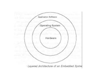
Figure 3.1 Embedded system Layered Architecture
The operating system runs above hardware and application software runs above operating system. Same architecture is applicable to any computer including a desktop computer. However, there will be significant differences. To have an operating system in every embedded system is not compulsory. There is no need for an operating system for small applications such as toys, remote control units, air conditioners, etc., and only software specific can be written to that application. It is advisable to have an operating system for applications that involve complex processing. You will also need to integrate the application software with the operating system and then transfer entire software onto the memory chip in such a case. Once the software is transferred to the memory chip, it will continue to run fora long time and one doesn’t need to reload new software. The various building blocks of the hardware of an embedded system are given below.
The building blocks of an embedded system are:
· The Central Processing Unit (CPU)
· Memory (RAM and ROM)
· The Input Devices
· The Output devices
· The Communication interface
· Specific circuitry depending on the application.
Central Processing Unit (CPU):
The Central Processing Unit can be any one of the following: microprocessor, microcontroller, or Digital Signal Processor. A micro-controller is nothing but a low-cost processor. Its main difference is that, it has many other components like memory, serial communication interface, analog-to digital converter etc on the chip itself. A micro-controller is the best choice for small applications as number of external components required will be very less. On the other hand, microprocessors are more powerful, but one need to use many external components along with them. For applications in which signal processing is involved such as video and audio processing, D5P is mainly used.
Memory:
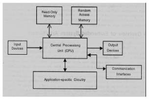
The memory can be categorized as Random Access Memory (RAM) and Read Only Memory (ROM). The memory of RAM will be erased if power is switched off to the chip. ROM will retain the contents even if the power is switched off. So, firmware is stored in the ROM. When power is switched on, the processor reads the ROM; the program is executed.
Fig 3.2 Embedded Architecture
Input devices: The input devices of an embedded system have very limited capability unlike the desktops. There is neither keyboard nor mouse, and hence interaction with the embedded system is not a simple task. Most of the embedded systems have a small keypad where you need to press one key to give a specific command. To only input the digits, a keypad is used. Most of the embedded systems used in process control do not have any input device for user interaction. The input is taken from the sensors and electrical signals that are produced are in turn fed to other systems.
Output devices:
The output devices of the embedded systems have very less capability. Few embedded systems have a fewLight Emitting Diodes (LEDs) whichindicate the health status of the system modules, or for thevisual indication of alarms. A small Liquid Crystal Display (LCD) can also be used to display theimportant parameters.
Communication interfaces:
The embedded systems need to, interact with other embedded systems as they may have to transmit data to a desktop. The embedded systems are provided with one or a fewcommunication interfaces like RS232, RS422, RS485, Universal Serial Bus (USB), IEEE 1394, Ethernet etc..,. .to facilitate this.
Application-specific circuitry:
Embedded systems may require sensors, transducers, special processing and control circuitry depending on its application. To carry out the necessary work this circuitry interacts with the processor. The entire hardware has to be given power supply either through the 230 volts main supply or through a battery. The hardware has to design in such a way that the power consumption is minimized.
HARDWARE IMPLEMENTATION OF THE PROJECT
In this chapter brief explanation about the Hardware Implementation of the project is done. We discuss the design and working of the design with the help of the block diagram. We explain the features, timer programming, serial communication, interrupts of 8051 microcontroller. We also explains the various modules used in this project.
4.1 Block Diagram of the Project and its Description:
The block diagram of the design is as shown in Figure 3.1. It consists of a power supply unit, microcontroller, Zigbee, RFID and MAX232 and LCD. The brief description of each unit is explained as follows.
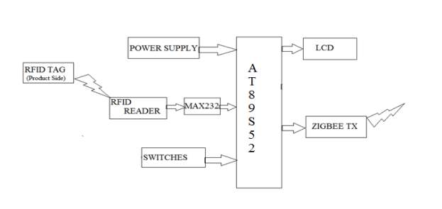
Figure 4.1 Trolley section
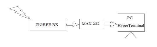
Figure 4.2 Counter section
4.2 POWER SUPPLY
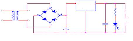
The input is given from regulated power supply shown in figure 3.2. The A.C. input (230V) from mains supply is stepped down by the transformer to 12V and is given to a rectifier. The output from the rectifier is a pulsating D.C voltage. To get a pure D.C voltage and to remove any A.C components that are present even after rectification, voltage at the output from the rectifier is fed to the filter. Now, this voltage is given to a voltage regulator to obtain a pure constant dc voltage.
In this project power supply requirement is to operate entire system. Every electronic device are operated using power supply only or stored supply like batteries. Using batteries is cost effective but power supply unit provides continuous supply from mains. So it is cheap one compared to batteries.


 vmsint


Transformer
Regulator
Rectifier
Filter
load


 To AC line Iout


 Vout
Vout


Figure 4.3 Components of power supply
4.2.1 Transformer:
Usually, to operate various electronic equipment, DC voltages 5V, 9V or 12V are used. These voltages maynot be obtained directly. Thus the a.c input available at the mains supply i.e., 230V must be brought down to the required voltage level as given above. This can be done by a transformer. Hence, a step down transformer is employed to decrease the voltage to the required level.
4.2.2 Rectifier:
The output of the transformer is led to the rectifier where it converts to A.C. into pulsating D.C. The rectifier can be a half wave rectifier or a full wave rectifier. Here, in this project, we use a bridge rectifier because of its merits like good stability and full wave rectification.
4.2.3 Filter:
Capacitive filter is also used in this project. The ripples from the output of rectifier are removed and the D.C. Until the mains voltage and load is maintained constant, output received and smoothened from this filter is constant. However, D.C. voltage received at this point changes if either of the two is varied. Therefore a regulator is applied at the output stage.
4.2.4 Voltage regulator:
Voltage regulator regulates the input applied to it. It is an electrical regulator which is designed to automatically maintain a constant voltage level. Here, in this project, the power supply of 5V and 12V are required. In order to obtain these voltage levels shown in figure 3.3, 7805 and 7812 voltage regulators are to be used. The first numbers -78 represents positive supply and the numbers- 05, 12 represent the required output voltage levels.
7805
Out
In
1
3
R1-330Ω
33330Ω
T1
2
5
104PF
C1
0-18V/25mA
LED
1000µF/25v
Diode Bridge
Figure 4.4 Power circuit diagram
4.3 MICROCONTROLLER (8052)
The widely used products in embedded system products are microcontrollers and microprocessors. Microcontroller is a device that can be programmed. A microcontroller has a CPU and a fixed amount of RAM, ROM, I/O ports and a timer embedded all on a single chip. The fixed amount of on-chip Read Only Memory, Random Access Memory and numerous Input/Output ports in microcontrollers makes them ideal for many applications in which cost and space are critical.
The Intel 8052 is Harvard architecture. It is a single chip microcontroller which was developed by Intel in 1980 for use in embedded systems. It has become popular in the 1980s and early 1990s, but today it has largely been superseded by a huge range of enhanced devices with 8051-compatible processor cores that are produced by more than 20 independent manufacturers including Atmel, Infineon Technologies and Maxim Integrated Products.
The CPU can work on only 8 bits of data at a time that means, 8052 is an 8-bit processor. Data larger than 8 bits must be broken into 8-bit pieces to be processed by the CPU. 8052 is available in different memory types such as UV-EPROM, Flash and NV-RAM.
4.3.1 Features of AT89S52:
• Re-programmable Flash Memory of 8K bytes.
• 256 bytes sized RAM.
• From 4.0V to 5.5V Operating Range.
• Fully Static Operation: from 0 Hz to 33 MHzs
• It has 3 level Program Memory Lock.
• It has 256 x 8-bit internal Random Access Memory.
• Consists 32 Programmable I/O Lines.
• 3 16-bit timers/counters are there.
• 8 Interrupt Sources are present.
• Full Duplex UART Serial Channel is available.
• Low-power Idle , Power-down Modes can be used.
• Interrupt recovery from the power down mode can be done.
• Watchdog timer is available.
• Dual data pointer exists.
• Power-off flag exists
• Speed programming time.
• Flexible ISP programming.
Description:
The AT89s52 microcontroller is a high-performance CMOS 8-bit microcomputer. It is a low voltage microcontroller. It consists of 8K bytes of Flash programmable memory. Manufacturing of this device is done using Atmel’s high density nonvolatile memory technology. It is compatible with industry-standard MCS-51 instructions set. The on-chip flash will allow to reprogram the program memory in the system or by a conventional non-volatile memory programmer. The Atmel AT89s52 microcontroller is a very powerful microcomputer, which is highly flexible and provides cost-effective solution to many embedded control applications by combining a versatile 8-bit CPU with a flash on a monolithic chip.
The AT89s52 microcontroller is designed with static logic for operation down to 0 frequency and it will support 2 software selectable energy saving modes. While allowing the Random Access Memory, timer(or)counters, serial port and interrupt system to continue functioning, the Idle mode stops CPU. The power-down mode will save the Random Access Memory contents but freezes the oscillator by disabling all other chip functions until next hardware reset is done.
4.3.2 Pin description:
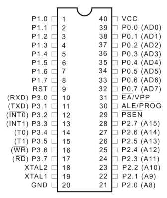
Figure 4.5 PIN diagram of 8052
Vcc : Pin 40 will provide required supply voltage to the chip. The voltage source is +5V.
GND : Pin 20 is the ground pin.
Port 0:
Port 0 is an 8-bit, open drain bidirectional I/O port. Each pin can take in eight TTL inputs as an output port. The port 0 pins are used as high impedance inputs when 1s are given to port 0 pins. Port 0 can also be configured to be the multiplexed low-order address/data bus during access to the external program and the data memory. In this mode, Port 0 has internal pull-ups.
Port 1:
Port 1 is an 8-bit port. It is a bidirectional I/O port. Port 1 has internal pull-ups. Its output buffers can sink/source 4 TTL inputs. They are pulled high by the internal pull-ups and can be used as inputs when 1s are given to Port 1 pins. As inputs, Port 1 pins that externally being pulled low will take current (IIL) due to the internal pull-ups. P1.0 and P1.1 pins of Port 1 can be configured to be the timer/counter 2 external count input (P1.0/T2) and the timer/counter 2 trigger input (P1.1/T2EX), respectively.
Port 2:
Port 2 is an 8-bit port. It is a bidirectional Input/Output port. It also has internal pull-ups. The Port 2 output buffers can sink/source 4 TTL inputs. They are pulled high by the internal pull-ups and can be used as inputs when 1s are written to Port 2 pins. As inputs, Port 2 pins that are externally being pulled low will source current (IIL) because of the internal pull-ups.
The port will also receive the high-order address bits and some control signals during Flash programming and verification process.
Port 3:
Port 3 is an 8-bit bidirectional Input/Output port. It has internal pull-ups. The output of Port 3 buffers can sink/source 4 TTL inputs. They are pulled high by the internal pull-ups and may be used as inputs when 1s are written to Port 3 pins. As inputs, Port 3 pins that are externally being pulled less will source current (IIL) due to the pull-ups. Port 3 receives some control signals for Flash programming and verification process.
Port 3 also serves the functions of various special features of the AT89S52 microcontroller..
RST:
Reset input A when high on this pin is given for 2 machine cycles while the oscillator is working resets the device. This pin works high for 98 oscillator periods after the Watchdog times out. The DISRTO bit in SFR AUXR (add 8EH) can be used to disable this feature. In default state of the bit DISRTO, the RESET HIGH out feature is enabled.
ALE/PROG:
Address Latch Enable is an o/p pulse for latching the lower byte of the address during accesses to the external memory. This pin is also the program pulse input during Flash programming.
In normal operation, ALE is emitted at a constant rate of 1/6 of the oscillator frequency and it may be used for external timing or clocking purposes.One ALE pulse is skipped during each access to the external data memory.
PSEN:
Program Store Enable is the read strobe to the external program memory. PSEN is activated twice for every machine cycle, except that 2 PSEN activations are skipped during every access to external data memory when the AT89S52 microcontroller executes code from the external program memory.
EA/VPP:
To enable the device to fetch code from the external program memory locations starting from 0000H up to FFFFH, external Access Enable( EA) must be strapped to Ground(GND). However, that if lock bit 1 is programmed, EA will be internally latched onto reset.
EA should be connected to VCC for internal program executions. This pin also receives the 12-volt programming enable voltage during the Flash programming.
XTAL1 and XTAL2:
XTAL1 is the input to the inverting oscillator amplifier and input to the internal clock operating circuit while XTAL2 is output from the inverting oscillator amplifier.
Special Function Registers:
User software should not write 1s to these unlisted locations, since they may be used in future products to provoke new features. In that case, the reset or the inactive values of the new bits will always be O.
Timer 2 Registers:
Control bits and the status bits are contained in the following registers- T2CON and T2MOD for Timer 2. The register pair RCAP2H, RCAP2L is the Capture (or) Reload register for Timer 2 in 16-bit capture mode or 16-bit auto-reload mode.
Interrupt Registers:
The individual interrupt enable bits are in the Interrupt Enable register. 2 priorities can be set for each of the six interrupt sources which are present in the IP register.
Dual Data Pointer Registers:
To facilitate the access to both internal and external data memory, 2 banks of 16-bit Data Pointer Registers are provided: DP0 at SFR address locations 82H-83H and DP1 at 84H and 85H. Bit DPS = O in SFR AUXR1 selects DPO and DPS = 1 selects DP1. The DPS bit should always be initialized to the appropriate value before accessing the respective Data Pointer Register.
Power off Flag (POF):
The Power off Flag is situated at bit 4 (PCON.4) in the PCON SFR. POF is set to “ONE” during power up. It can be set and reset under software control and is not affected by reset condition.
Memory Organization:
MCS-51 devices have a separate address space for Program Memory and Data Memory. Upto 64K bytes each of external Program and Data Memory can be addressed.
Program Memory : If the EA pin is connected to Ground(GND), all program fetches are directed towards external memory. On the AT89S52, if EA is connected to supply (VCC), program fetches to addresses from 0000H through 1FFFH are directed to internal memory and fetches to addresses 2000H through FFFFH are to external memory.
Data Memory: The AT89S52 implements 256 bytes of on-chip RAM. The upper 128 bytes occupy a parallel address space to the Special Function Registers. This means that the higher 128 bytes have the same addresses as the SFR space but are physically separate from the SFR space.
UART:
The Atmel 8051 Microcontrollers implement 3 general purpose, 16-bit timers (or) counters. They are identified as Timer 0, Timer 1 and Timer 2 and can be independently configured to operate in a number of different modes as a timer or as an event counter.
The 4 operating modes are Timer 2, has 3modes of operation: ‘capture’, ‘auto-reload’ and ‘baud rate generator’.
Interrupts:
The AT89S52 will have a total 6 interrupt vectors: 2 external interrupts (INTO and INT1), 3 timer interrupts (Timer 0, Timer 1 and Timer 2) and the serial port interrupt. These interrupts were all shown in the above figure.
By setting or clearing a bit in Special Function Register IE, each of these interrupts can be enabled or disabled individually. IE also contains a global disable bit, represented as EA, which disables all the interrupts at a time. User software should not write a 1 to this bit position, since it may be used in future AT89 products.
Crystal oscillator:
The 8051 uses the crystal oscillator to synchronize its operation. The 8051 operates efficiently using “machine cycles” . The Minimum time taken to execute a single 8051 instruction is a single cycle. Many such instructions take multiple cycles. 8051 consists of an on-chip oscillator. It needs an external crystal to decide the operating frequency of 8051. The crystal is connected to pins 18 and 19 with stabilizing capacitors. 12 MHz (11.059MHz) crystal is often used and the capacitance ranges from 20pf to 40pf.
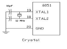
Figure 4.6 Crystal Oscillator Circuit
Reset :
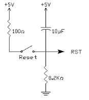
Figure 4.7 Reset Pin Circuit
RESET is an active High input When RESET is set to High, 8051 goes back to the power on state. The 8051 is reset by holding the RST high for at least two machine cycles and then returning it low. Initially charging of capacitor makes RST High, when capacitor charges fully it blocks DC.
SIP Resistor: SIP resistor is a single in pack Resistor (i.e.,) 8 resistors are connected together in series. Basically SIP resistor is a 9 pin connector in which the first pin is for power supply to the entire 8 resistors in SIP. Generally SIP Resistor is used to discconnect the open drain connections of Port 0.
4.4. RFID Reader:
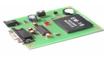
Figure 4.8 RFID Reader
Radio Frequency Identification (RFID) Card Reader gives a very low-cost solution to read the passive RFID transponder tags that are upto 7 cm away. RFID Card Readers applications include a wide range of hobbyist and commercial applications, including access control, automatic identification, robotics navigation, inventory tracking, payment systems, and car immobilization. The RFID card reader reads the RFID tag in range and outputs unique identification code of the tag at baud rate of 9600.The data from RFID reader is interfaced and read by the microcontroller or Computer terminal.
What is RFID?
A basic RFID system consists of the following three components:
a) An antenna or a coil
b) A transceiver (with decoder)
c) A transponder (RF tag)
They are electronically programmed with the unique information. There are many different types of RFID systems out in the market. They are categorized according to their frequency ranges. Few of the most commonly used RFID kits are:
- Low-frequency (30 KHz to 500 KHz)
- Mid-Frequency (900KHz to 1500MHz)
- High Frequency (2.4GHz to 2.5GHz)
These frequency ranges mostly show the RF ranges of the tags from low frequency tag ranging from 3m to 5m, mid frequency ranging from 5m to 17m and high frequency ranging from 5ft to 90ft. The cost of the system is based according to their ranges with low-frequency system ranging from a few hundred dollars to a high-frequency system ranging somewhere near 5000 dollars.
Radio Frequency Identification (RFID) Card Readers provide a low-cost solution to read passive RFID transponder tags up to 2 inches away.
Features:
- Low-cost method for reading the passive RFID transponder tags
- 9600 bps serial interface at RS232 level
- Buzzer & LED that indicate valid RFID Tag detection
- RS232 interface that is connected directly to PC, Mac or Linux machine requires no additional wiring.
RFID Reader Package Includes
RFID Reader (Assembled & Tested with 1 year warranty)
Serial Cable
Information: Each transponder tag contains a unique identifier (one of 240, or 1,099,511,627,776 possible combinations) that is read by the RFID Card Reader and transmitted to the host via a simple serial interface. It means no two tags are same. Each tag has different value. This value if read by reader.
Communication
When the RFID Card Reader is active and a valid RFID transponder tag is placed within range of the activated reader, the unique ID will be transmitted as a 12-byte printable ASCII string serially to the host in the following format:
Using RFID Reader:
When powered on, the RFID reader will activate an RF field waiting for the tag to come into its range. Once the tag is detected, its unique ID number is read and the data is sent via a serial interface. The valid tag detecting is indicated by an LED blink and the Buzzer beep. Face of the RFID tag must be held parallel to the front of the antenna (where majority of RF energy is focused). On PC, software like hyper terminal which can show ASCII data at 9600 baud rate can be used. One can also develop software in any language which can connect to serial port and listen for the incoming ASCII data.
Power Requirement of Receiver: The unit needs around 200mA power to operate at 12V. You can use any readymade 12V 500mA DC Adapter or design a transformer plus rectifier based 12V DC power for the board. You can also use just the 12V transformer as the board has bridge and capacitor to convert to DC. Serial Cable connections for RS232 interfacing (Provided with product) To use with a PC serial port, use a serial cable of male-female type with pins 2,3,5 connected to 2,3,5 straight(no cross over cable).
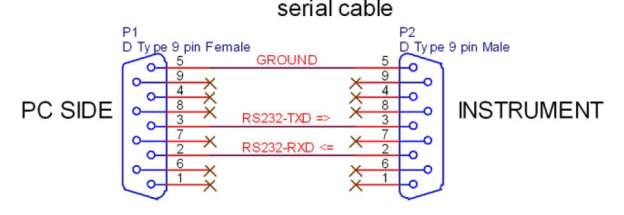
Figure 4.9 RFID power requirement
Connecting to PC
Utilize the provided serial link to interface with PC’s serial port. Utilize Hyperterminal programming which accompanies Windows XP or utilize whatever other Terminal programming with taking after settings.
Information Rate: 9600 Data Bits: 8 Parity: None Stop Bit: 1 Flow Control.
Parts OF RFID:
An essential RFID framework comprise of the accompanying three segments:
1) An recieving wire or curl
2) A handset (with decoder)
3) A transponder (RF tag) electronically modified with extraordinary data
Reception apparatus
To actuate the tag and read and compose information to it outside Access Enable EA must be strapped to GND. Recieving wires are the conductors between the tag and the handset, which controls the framework’s information securing and correspondence. Reception apparatuses are accessible in assortments of shapes and sizes; they can be incorporated with a door jamb to get label information from people or things going through the entryway, or mounted on an interstate tollbooth to screen movement going by on an expressway. Contingent on its energy yield and the radio recurrence utilized the peruser produces radio waves in scopes of somewhere in the range of one inch to 100 feet or more. It distinguishes the peruser’s enactment flag when a RFID label goes through the electromagnetic zone,. The peruser additionally deciphers the information encoded in the label’s coordinated circuit (silicon chip) and the information is passed to the host PC for preparing.
Figure 4.10 RFID Antenna
Labels (Transponders)
A RFID label includes a microchip that contains recognizing data and a recieving wire that will transmit this information remotely to a peruser. The chip will contain a serialized identifier, or tag number, that particularly recognizes that thing, like the way many standardized identifications are utilized today. Be that as it may, a key distinction is that RFID labels have a higher information limit than their scanner tag partners. The time and date of proprietorship exchange or refreshing the repair history of a settled resource are the cases for last ability. While these are the most exorbitant of the three label sorts and are not functional for following reasonable things, future guidelines for electronic item codes (EPC) seem, by all accounts, to be traveled toward this path.
Figure 4.11 RFID TAGS
Frequencies: There are an assortment of frequencies or spectra through which RFID labels can speak with perusers like every single remote correspondence. There are additionally exchange offs among cost, execution and application necessities.
EPC Tags: EPC alludes to “electronic item code,” a rising determination for RFID labels, perusers and business applications initially created at the Auto-ID Center at the Massachusetts Institute of Technology.
RF TRANSCEIVER:
The RF handset is the wellspring of RF vitality used to actuate and control the latent RFID labels. The RF handset might be encased in an indistinguishable bureau from the peruser or might be in a different bit of gear. The handset is regularly alluded to as a RF module when given as a different bit of gear.
Typical Applications for RFID include:
- Automatic Vehicle identification
- Inventory Management
- Work-in-Process and Progress
- Container or Yard Management
- Document tracking or Jewellery tracking
- Patient Monitoring in medical stream.
The Advantages of RFID Over Bar Coding:
- There are no “line of sight” requirements: Bar code reads can sometimes be limited or problematic due to the need to have a direct “line of sight” between a scanner and a bar code but RFID tags can be read through materials without line of sight.
- They have greater data capacity: RFID tags can be easily encoded with the product details such as lot and batch, weight, etc.
- It has “Write” capabilities: Because RFID tags can be rewritten with new data as supply chain activities are completed. As they move throughout the supply chain tagged products carry updated information.
Common Problems with RFID: Reader collision and tag collision are some common problems with RFID. When the signals from two or more readers overlap reader collision occurs.
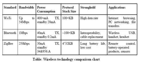
4.5  Zigbee Technology:
Figure 4.12 ZIGBEE
Introduction to Zigbee:
- Zigbee is an IEEE 802.15.4 standard for information correspondences with business and shopper gadgets. Enabling batteries to basically keep going forever it is planned around low-control utilization. The Zigbee standard gives system, security and application bolster administrations working on top of the IEEE 802.15.4 Medium Access Control (MAC) and Physical Layer (PHY) remote standard. Zigbee utilizes a suite of innovations to empower versatile, self-sorting out, self-recuperating systems that can oversee different information activity designs.
- The present rundown of use profiles either distributed or in progress are as per the following:
- Home Automation
- Zigbee Smart Energy
- Telecommunication Applications
- Personal Home
- Why is Zigbee required?
- To deliver mid to high information rates for voice, PC LANs, video, etc.,.there are a huge number of gauges. Be that as it may, up till now there hasn’t been a remote system standard that meets the one of a kind needs of sensors and control gadgets. Sensors and controls needn’t bother with high data transfer capacity however they do require low inertness and low vitality utilization for long battery lives and for expansive gadget clusters.
- Zigbee is ready to end up noticeably the worldwide control/sensor arrange standard. It has been intended to give the components given underneath:
- Very low power utilization, essentially actualized.
- Generally, clients anticipate that batteries will last numerous months to years. Think about that as a normal single family house has around 6 smoke/CO identifiers. In the event that the batteries for every one just kept going six months, the property holder must supplant batteries consistently.
- Depending upon your idleness and power necessities, for example, sniff, stop, hold, dynamic, and so on bluetooth has a wide range of modes and states. Zigbee/IEEE 802.15.4 has dynamic (transmit/get) or rest. Application programming needs to concentrate on the application, not on which control mode is ideal for every part of operation.
- Even mains controlled gear should be aware of vitality. Consider a future home with 100 remote control/sensor gadgets,
- Zigbee gadgets will be more environmental than its forerunners sparing megawatts at it full sending.
- Very minimal effort.
- High thickness of hubs for each network.Zigbee’s utilization of the IEEE 802.15.4 PHY and MAC enables systems to deal with any number of gadgets. This quality is basic for huge sensor clusters and control systems.
- Simple convention and worldwide usage.
4.5.1 ZigBee/IEEE 802.15.4 – General Characteristics
- Dual PHY (2.4GHz and 868/915 MHz) exists.
- Data rates of 250 kbps (@2.4 GHz), 40 kbps (@ 915 MHz), and 20 kbps (@868 MHz) can be utilized.
- Has Multiple topologies: star, distributed, workAddressing space of up to:
- About 18,450,000,000,000,000,000 devices (64 bit IEEE address)
- Upto 65,535 networks
- Optional guaranteed time slot for applications which require low latency
- It has a Fully hand-shaked protocol for transfer reliability
- Range: from 50m typical (5-500m based on environment)
4.5.2 Architecture:
Zigbee is a home area network that is designed specifically to replace the proliferation of individual remote controls.To satisfy the market’s need for a cost effective, standards based wireless network that supports low data rates, low power consumption, security and reliability,Zigbee was created. The ZigBee Alliance, an industry working group (www.zigbee.org), is developing standardized application software on top of the IEEE 802.15.4 wireless standard.
The IEEE 802.15.4 PHY and MAC along with Zigbee’s Network and Application Support Layer provide:
- Very low cost
- Easy to implement
- Reliable data transfer is possible
- Short range operation
- Extremely low power consumption
- Appropriate levels of security
Network Routing Overview:
ZigBee directing calculation is as various leveled steering system with table-driven improvements connected any place conceivable.
It begun with all around concentrated open area calculation AODV and Motorola’s Cluster-Tree calculation and furthermore from collapsing in thoughts from Ember Corporation’s GRAd.
Organize Summary:
The system layer will expand upon the IEEE 802.15.4 MAC’s elements permitting the augmentation of scope. More bunches can be included. The systems can be solidified or part up.
Application layer:
The ZigBee application layer is involved APS sub-layer, the ZDO and the producer characterized application objects. The other duty of the APS sub-layer is disclosure, which is the capacity to figure out which different gadgets are working in the individual working space of a gadget.
Application Support Layer: This layer gives the accompanying administrations:
• Discovery: The capacity to figure out which different gadgets are working in the individual working space of a gadget.
• Binding: The capacity to match at least two gadgets together in light of their administrations and their needs and sending messages between bound gadgets
4.6 MAX 232
Max232 IC is a specialized circuit that makes standard voltages as required by RS232 standards. MAX232 IC provides best noise rejection .It is very reliable against discharges and short circuits. MAX232 IC chips are commonly referred to as line drivers.
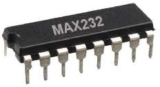
Figure 4.13 MAX232 IC
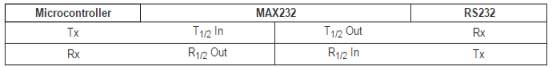
The baud rate and voltage levels of Microcontroller and PC should be the same to ensure data transfer between PC and microcontroller. The voltage levels supported are logic1 and logic 0 i.e., logic 1 is +5V and logic 0 is 0V. But for PC, RS232 voltage levels are considered and they are: logic 1 is taken as -3V to -25V and logic 0 as +3V to +25V. So, in order to equal these voltage levels, MAX232 IC is used. Thus this IC converts RS232 voltage levels to microcontroller voltage levels and vice versa.
Pin Configuration and Functions:
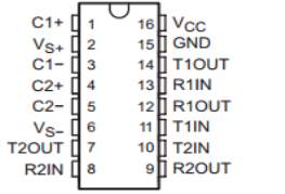
Figure 4.14 pin diagram of MAX 232
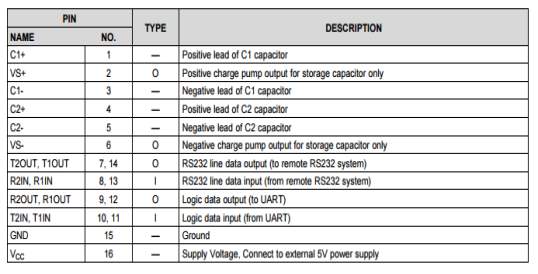
Table 4.2: Pin Description of MAX 232
To convert the TTL/CMOS logic levels to RS232 logic levels during the serial communication of the microcontrollers with PC, MAX232 IC is used. The controller operates at TTL logic level (0-5V) and the serial communication in PC works on RS232 standards (-25 V to + 25V). They convert the TTL/CMOS input level into RS232 level. The input of the transmitter is taken from controller’s serial transmission pin and the output is sent to RS232’s receiver. The receivers, at the same time, take input from the transmission pin of RS232 serial port and give the serial output to microcontroller’s receiver pin. MAX232 needs 4 external capacitors whose value ranges from 1µf to 22µf.
Features
- A Single 5-V Power Supply With 1.0-µF Charge-Pump Capacitors are used for operation
- Upto 120 kbit/s operation.
- Consists of two Drivers and two Receivers
- Upto ±30-V Input Levels
- It has low Supply Current: 8 mA Typical
Applications
- In TIA/EIA-232-F
- Used in Battery-Powered Systems
- Used in Terminals
- Used in Modems
- Used in Computers
4.7. Switches and Pushbuttons:
The simplest way of controlling appearance of some voltage on microcontroller’s input pin is by using switches and pushbuttons. There is no need for additional explanation of how these components operate.
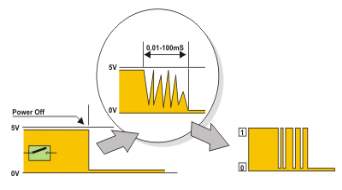
Figure 4.15 Switch functionality
This is something commonly unnoticeable when using these components in everyday life. It is about contact bounce, a common problem with mechanical switches. The values of elements are not strictly determined since the bouncing time is not defined. The values shown on figure are sufficient in the most cases,.
Switch Interfacing with 8052:
In 8051 all the ports have internal 10k Pull-up resistors except PORT 0. Hence PORTs1, 2 & 3 can be directly used to interface with a switch whereas an external 10k pull-up resistor is required for PORT 0 to be used for switch interfacing or for any other input. Fig. 1 shows switch interfacing for PORTs 1, 2 & 3. Fig 2 shows switch interfacing to the remaining port, PORT 0.
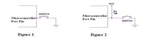
For any pin to be used as an input pin, a HIGH (1) should be written to the pin if the pin will always to be read as LOW. When the switch is not pressed in the above figure, the 10k resistor provides the current needed for LOGIC 1 and closure of switch provides LOGIC 0 to the controller PIN.
LIQUID CRYSTAL DISPLAY
LCD is the acronym for Liquid Crystal Display. LCD is finding wide spread use replacing LEDs (seven segment LEDs or other multi segment LEDs) because of the following reasons:
- Reducing prices of LCDs.
- In contrast to LEDs, LCD’s ability to display numbers, characters and graphics which are limited to numbers and a few characters.
- Incorporation of a refreshing controller into the LCD, thereby relieving the CPU of the task of refreshing the LCD. In contrast, the LED must be refreshed by the CPU to keep displaying the data.
- Ease of programming for characters and graphics.
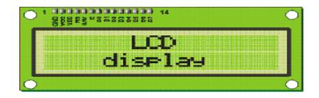
Figure 4.16 LCD display
4.8.1. Pins Functions Pins are there along one side of the small printed board that are used for connection to the microcontroller. There are a total of 14 pins marked with numbers (16 in case the background light is built in). Their function is described in the table given below.
Table 4.2 PIN functions of LCD
| Pin No | Function | Name |
| 1 | Ground (0V) | Ground |
| 2 | Supply Voltage, 5V(4.7 V-5.3V) | Vcc |
| 3 | Contrast adjustment, through a variable resistor | VEE |
| 4 | Selects command register when low, and the register when high | Register select |
| 5 | Low to write to the register, high to read from the register | Read /Write |
| 6 | Sends data to data pins when a high to low pulse is given | Enable |
| 7 | DB0 | |
| 8 | DB1 | |
| 9 | DB2 | |
| 10 | 8- BIT DATA PINS | DB3 |
| 11 | DB4 | |
| 12 | DB5 | |
| 13 | DB6 | |
| 14 | DB7 | |
| 15 | Backlight Vcc(5V) | Led + |
| 16 | Backlight ground(0V) | Led+ |
- LCD screen:
Every character comprises of 5×7 dot matrix. Contrast on the display will depend on the power supply, voltage and also whether messages are displayed in one or two lines. For that reason, variable voltage O-Vdd is applied on pin that is marked as Vee. Trimmer potentiometer is usually used for that purpose. When used during operating, a resistor for current limitation should be used


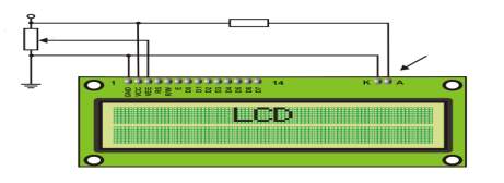
Figure 4.17 LCD connection
4.8.3. LCD Basic Commands :All data transferred to LCD through outputs D0-D7 will be interpreted as commands or as data, which depends on logic state on pin RS: RS = 1 – Bits D0 – D7 are addresses of characters that should be displayed. List of commands which LCD recognizes are very important to write the code for LCD. The below table 3.4 shows the LCD commands which are useful in the writing of code to display the data.
Table 4.3 LCD commands table
| Command | RS | RW | D7 | D6 | D5 | D4 | D3 | D2 | D1 | D0 | Execution
Time |
|
| Clear display | O | O | O | O | O | O | O | O | O | 1 | 1.64Ms | |
| Cursor home | O | O | O | O | O | O | O | O | 1 | X | 1.64mS | |
| Entry mode set | O | O | O | O | O | O | O | 1 | I/D | S | 4OuS | |
| Display on/off control | O | O | O | O | O | O | 1 | D | U | B | 4OuS | |
| Cursor/Display Shift | O | O | O | O | O | 1 | D/C | R/L | X | X | 4OuS | |
| Function set | O | O | O | O | 1 | DL | N | F | X | X | 4OuS | |
| Set CGRAM address | O | O | O | 1 | CGRAM address | 4OuS | ||||||
| Set DDRAM address | O | O | 1 | DDRAM address | 4OuS | |||||||
| Read “BUSY” flag (BF) | O | 1 | BF | DDRAM address | – | |||||||
| Write to CGRAM or DDRAM | 1 | O | D7 | D6 | D5 | D4 | D3 | D2 | D1 | D0 | 4OuS | |
| Read from CGRAM or DDRAM | 1 | 1 | D7 | D6 | D5 | D4 | D3 | D2 | D1 | D0 | 4OuS | |
I/D 1 = Increment by 1 R/L 1 = Right shift
0 = Decrement by 1 0 =Left shift
S 1 = Display shift is on DL 1 = 8-bits interface
0 = Display shift is off 0 = 4-bits interface
D 1 = Display is on N 1 = Display in two lines
0 = Display is off 0 = Display in one line
U 1 = Cursor is on F 1 = Character format is 5×10 dots
0 = Cursor is off 0 = Character format is 5×7 dots
B 1 = Cursor blink is on D/C 1 = Display shift is done
0 = Cursor blink is off 0 = Cursor shift is done
4.8.4. LCD Connection
Depending on how many lines are used for connection to microcontroller, 8-bit and 4-bit LCD modes are there. The appropriate mode is determined at the beginning of the process in a phase called “initialization”. In the first case, the data are transferred through outputs D0-D7 as it has been already explained. LCD will correctly connect and interpret each data received with the help of initialization. With regards to the fact that data are rarely read from LCD (data mainly are transferred from microcontroller to LCD) one more I/O pin may be saved by simple connecting R/W pin to the Ground. Such saving has its price. Even though message displaying will be normally performed, it will not be possible to read from busy flag since it is not possible to read from display.
4.8.5. LCD Initialization:Once the power supply is turned on, LCD is automatically cleared. This process lasts for approximately 15mS. After that, display is ready to operate. The mode of operating is set by default. This means that:
1. Display is cleared
2. Mode
DL = 1=> Communication through an 8-bit interface is done.
N = 0 =>Messages are displayed in one line
F = 0 =>Character font is 5 x 8 dots
3. Display/Cursor on/off
D = 0 Display is off
U = 0 Cursor is off
B = 0 Cursor blink is off
3. Character entry
ID =1=> Addresses on display are automatically incremented by one
S = 0 =>Display shift is off
Mainly, Automatic reset is performed without any problem.
4.8.6. Contrast control
To have a clear view of the characters on the LCD, contrast should be adjusted. As the voltage of this preset is varied, the contrast of the LCD can be adjusted.


Wiper
Track
Terminals
Figure 4.19 Variable resistor
4.8.7. Presets
Presets are miniature versions of the standard variable resistor. They are designed to be mounted directly onto the circuit board and are adjusted only when the circuit is built. To move the slider from one end of the track to the other, giving very fine control the screw must be turned many times (10+) .

Figure 4.19 Preset symbol
SOFTWARE IMPLEMENTATION
This chapter briefly explains about the firmware implementation of the project
5.1. SOURCE CODE
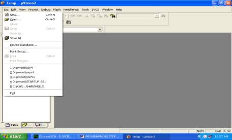
- Click on the Keil uVision Icon on Desktop
- The following figure will appear
- Click on Project menu on the title bar
- Click on New Project icon.
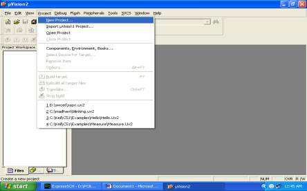
- Save the Project by giving suitable project name with an extension in your own folder situated in either C: or D:
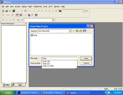
- Click on Save button above. The project is saved now.
- Select component for your project. i.e. Atmel.
- Click + Symbol beside Atmel .
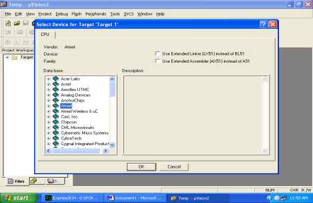
- Select AT89C51 as shown in the figure below
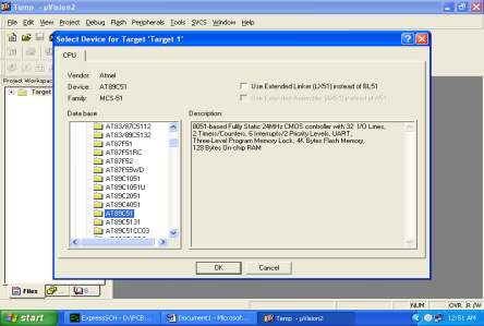
- Then Click “OK”
- The figure will appear as shown below
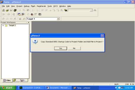
- Click either YES or NO…mostly it is a “NO”
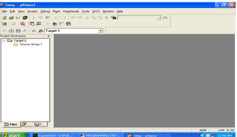
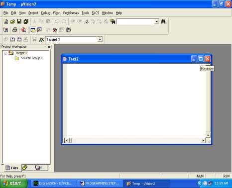
- Now your project is ready to be used.
- Now double click on Target1, you will get another option “Source group 1” as shown in next image.
- Click on the file option from the menu bar and select “new”
- The next screen will be as shown in next page, and just maximize it by double clicking on its blue boarder.
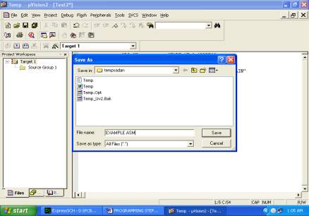
- Now start writing program in either in “C” program or “ASM”
- For a program written in Assembly, save it with extension “. asm” and for the one saved in“C” based program save it with extension “ .C”
- Now right click on Source group 1.Click on “Add files to Group Source”
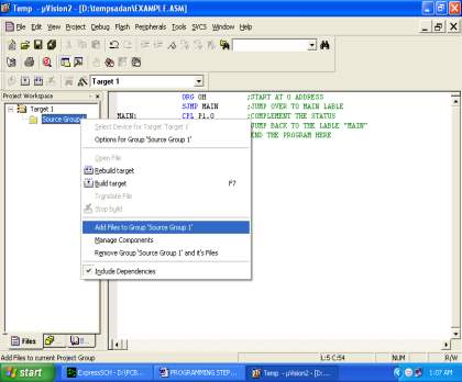
- Now we will see another window, on which by default “C” files appear.
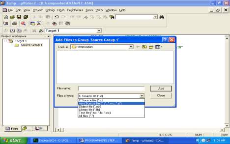
- Now select your file extension given while saving the file
- Click only one time on the option “ADD”
- Now Press function key F7 for compilation. Error will appear if so happened.
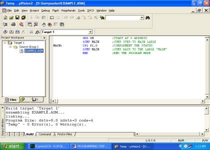
- If the file contains no error, then press Ctrl+F5 simultaneously.
- The new window looks as follows
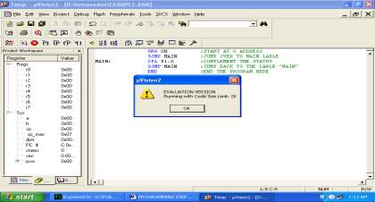
- Then Click “OK”
- Now Click on the Peripherals from menu bar, and check your required port as shown in fig below
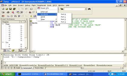
- Drag the port a side and click in the program file.
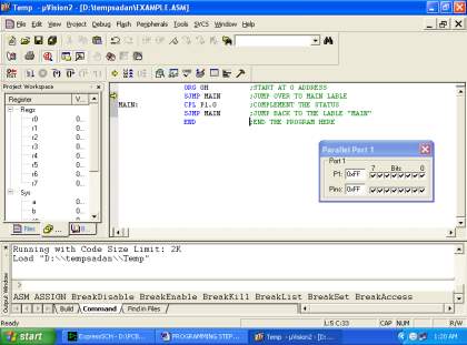
- Now keep Pressing function key “F11” slowly and observe.
- You are running your program successfully
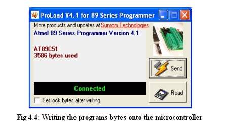
5.2. Proload
Proload software accepts only hex files. Hex code has to be dumped into the microcontroller after converting the machine code into Hex code and this is done by the Proload. Proload is a programmer that itself contains a microcontroller in it other than the one which is to be programmed. This programmer kit contains a power supply section in the board itself but a source is required to switch on that power supply. This can be accomplished from the power supply board which has an output of 12volts.
Features:
- It will support major Atmel 89 series devices
- It will identify connected hardware and devices automatically.
- It erases before writing and verifies after writing automatically
- Status bar provides information and gives access to latest programmed file
- It is simple and Easy to use
- Works with 57600 speed
Description:
Software is easy to use and is of very low cost, and it is a very powerful flash microcontroller programmer for the Atmel 89 series. This software will Program, Read the code and Verify the code Data, writhes the Lock Bits, erase and blank check. All the fuse and lock bits are programmable. Using a standard RS232 serial port, it connects to a host computer. All the programming ‘intelligence’ is already built into the programmer and you do not need any special hardware to run the program. For easy programming of the devices, Programmer must come with window based software.
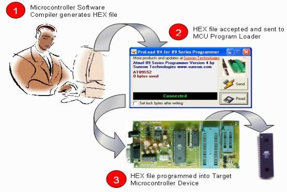
Programming Software:
‘Proload V4.1’ software is executed which accepts the Intel HEX format file which is generated from compiler and sent to the target microcontroller. It will automatically detect the hardware connected to the serial port. It will also detect the chip inserted and bytes used automatically. This software was developed in Delphi 7 and it requires no overhead of any external DLL.
5.3 Flow chart
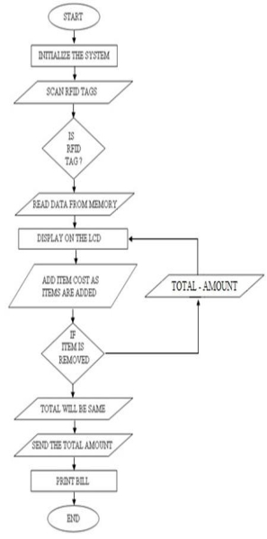
RESULTS AND DISCUSSIONS
6.1 IMPLEMENTATION RESULT
The implementation of realization of “Automated Smart Trolley with Smart Billing Using AT89S52 Controller” is implemented successfully. Without any interference between different modules in the design, the communication is properly implemented. It is designed to meet all the specifications and requirements as well.
The circuit is implemented in Orcad and on the microcontroller board. The performance of the device has been verified in both software simulator as well as hardware design. The total circuit is verified functionally and it is following the application software. Conclusions are that the design implemented in the present work provide portability, flexibility and the data transmission is also done with very low power consumption.
The output images can be seen as shown below.
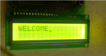
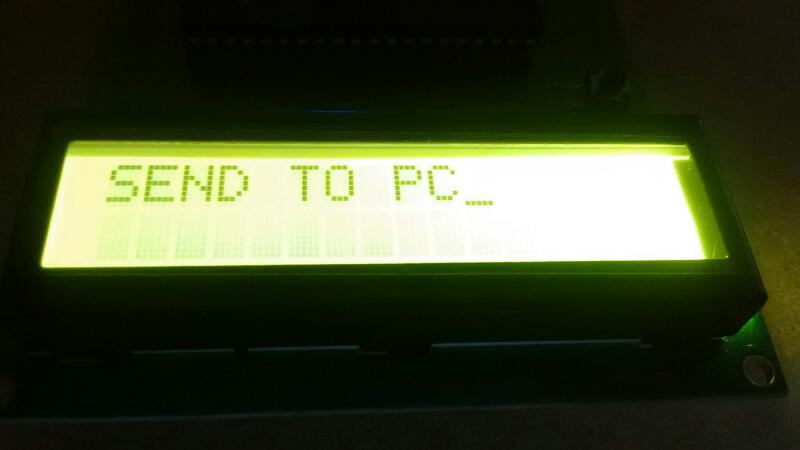
1. In the beginning, when the kit is switched on by providing the power supply to the kit, the below images are seen which show “WELCOME” on the LCD screen of the device.
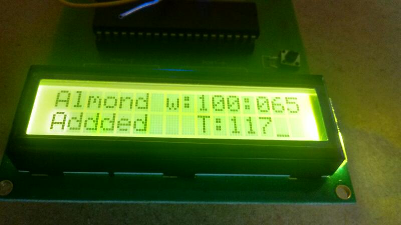
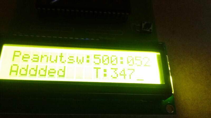
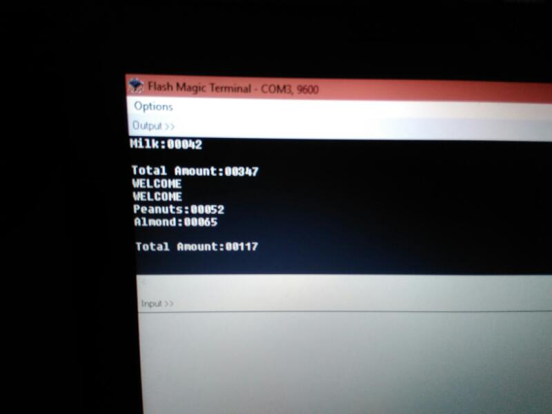
2 .When an RFID tag is scanned by the RFID reader, the images as shown below are displayed along with the details of the name of the product, weight of the product, cost of the product and the total billing amount.
- After completion of the shopping, press the shopping completed button. The image as shown below is seen and the information is sent to the PC using ZIGBEE technology.
- The items with their individual costs and the total cost is displayed on the PC as shown in the below image.
6.2 ADVANTAGES
- Easy to use and reduces man power.
- Safe, secured and needs low power.
- It is echo friendly; with this we can eliminate usage of paper.
- It very attractive and eye catching.
- Easy to shop
- Easy to use
- Flexible
6.3 APPLICATIONS
- Shopping applications
- Industrial application, etc
CONCLUSION AND FUTURE SCOPE
7.1 CONCLUSION
The intended objectives were successfully achieved in the prototype model developed. The developed product is easy to use, economical and does not require any special training. This project simplifies the billing process, makes it swift & increases the security using RFID technique. This will take the overall shopping experience to a different level.
7.2 FUTURE SCOPE
In future, we can pay the bill amount via online by using the smart phone by scanning the QR code of that particular supermarket. And get the soft copy of the bill receipt to check out from the super market.
REFERENCES
[1] www.schneiderelectric.com.hk/resources/access/text/rfidreader
[2] http://archive.computerhistory.org/resources/access Oral History Panel, retrieved 2011 June 28 page 4
[3] Microchip PIC16C84, a reprogrammable EEPROM-based 8-bit microcontroller 1993
[4] 8052 microcontrollers: an applications-based introduction
[5] BBC, (2003), Supermarket Tries Out Smart Tagging, BBC News, www.bbc.co.uk, 16 January.
[6] www.schneiderelectric.com.hk/…/Sympholux_Shopping_Mall
[7] RFID JOURNAL, 2002-2007, REFFERD 6.8.2007, http://www.rfidjournal.com [8] http://www.vbtutor.net/vb6/vbtutor.html visual basic 6 tutorial
ANNEXURE
#include#include #define lcd_data P2 sbit lcd_rs=P2^0; sbit lcd_en=P2^1; void delay(unsigned int ch) //delay function { unsigned int i=0,j=0; for(i=0;i
Cite This Work
To export a reference to this article please select a referencing stye below:
Related Services
View all


Related Content
All TagsContent relating to: "Information Systems"
Information Systems relates to systems that allow people and businesses to handle and use data in a multitude of ways. Information Systems can assist you in processing and filtering data, and can be used in many different environments.
Related Articles

DMCA / Removal Request
If you are the original writer of this dissertation and no longer wish to have your work published on the UKDiss.com website then please: