Green Synthesis of CdSe nanoparticle by Different Leaves Extract: Variation in Particle Size
Info: 9085 words (36 pages) Dissertation
Published: 9th Dec 2019
Tagged: SciencesEarth Sciences
Chapter 1
1.1 Introduction
“Nanotechnology related to design, characterisation, production and application of different structure, devices and systems by controlling the shape and size in the nanometre scale” [1].
Richard Feynman is known as the father of nanotechnology. According to National Nanotechnology Initiative (NNI) US, there are three aspects of nanotechnology: (i)At the macromolecular, molecular or atomic levels technology and research development (ii) With novel properties and functions of devices, structures and systems its applications and development are due to their small and intermediate size (iii) At the atomic scale control and manipulation of materials [2].
Nano materials having range in between 1 to 100 nm, one nanometre is equal to one billionth of metre [3]. Because of the small size of the particles various properties changes like reactivity ,optical property, electrical property, chemical property, physical property. These changes in property are obtain by reducing the size of the particles below a certain critical size [4].
There is the change in the nanoparticles properties are due to two reasons, firstly there is increase in surface to volume ratio with decreasing in the size of the particles and secondly there is electronic structure of the materials changes which are due to quantum confinement effects [5]. With size of the semiconductor nanoparticles an interesting effect of change in the electronic structure is seen with the variation of the band gap. As we decreases the size of the particles band gap of the material gets increased. According to requirements we are able to use them. Scientific enthusiasm about the nature of nano particles and possible applications of these nano-materials are revolutionizing and this can bring many benefits all over the world [6] .
1.2 Nanoparticles
A small particle that behaves as a whole unit in the terms of its transport and properties are defined as nanoparticles [7]. According to size particles are further classified: which is in the range between 100 and 2500 nanometres, fine particles are cover in the terms of diameter. On the other hand, between in the range of 1 and 100 nanometres ultrafine particles are sized. Nanoparticles are sized between 1 and 100 nanometres which are similar to ultrafine particles [8].
Size-related properties those observed in bulk materials or fine particles, nanoparticles may or may not exhibit that properties makes nanoparticles differ significantly [9]. Comparison in size of a cell (10–100μm), a virus (20–450 nm), a protein (5–50 nm) or a gene (2 nm wide and 10–100 nm long) nanoparticles are smaller in size [10] . The bridge between bulk materials, molecules and structures at atomic level represented by nanoparticles which drawn great interest [11]. Nanoparticle research is currently an area of intense scientific interest due to a wide variety of potential applications in biomedical, optical and electronic fields [12].
Because of small size of nano particles they are most efficient to use them, gives better results; therefore they are used in wide varieties of applications.
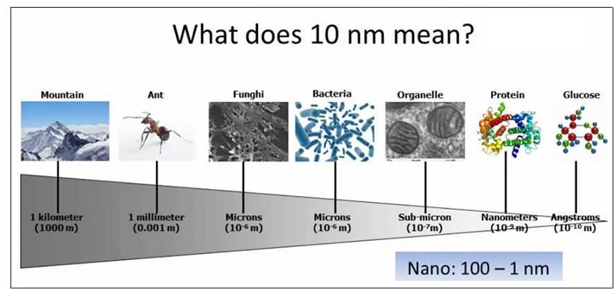
Fig (1.1) What does 10 nanometer means
1.3 CLASSIFICATION OF NANOPARTICLES
With nanoscale dimensions we can obtained all conventional materials like metals, polymers, semiconductors , glass or ceramic. In nanomaterials the spectrum ranges widely from inorganic or organic, crystalline or amorphous, these can be found as solo particles, aggregates, in a matrix form powders or dispersed, suspensions and emulsions, over colloids, Nano layers and films, class of fullerenes and their different derivatives [13]. For the classification of nanomaterials there are several verious approaches such as on the basis of dimensions, phase composition and manufacturing process [14].
a) On the Basis of Dimension
On the basis of dimensionality, these materials can be classified into three different categories which are classified as follows:
- One-dimensional (1D) or layered or lamellar structures, in which the magnitudes of length and width are much greater than the thickness that is only a few nanometres in size.
- Two-dimensional (2D) or rod-shaped or filamentary structures, in these materials the length is substantially larger than width or diameter, which are of nanometre dimensions.
- Three-dimensional (3D) or equiaxed or crystallite nanostructured materials, these are the materials in which all the three dimensions are of nanometre size and are termed as nanostructured crystallites [15]
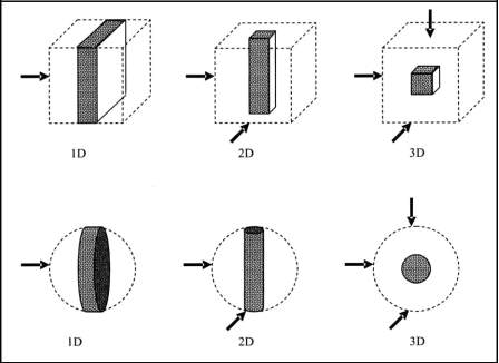
Fig (1.2) Confinement in the different dimensions
B) On The Basis of Phase Composition[16]
Actually phase represents the “state of matter”, with variation of temperature, pressure and composition phase of material changes. Different state of matters described by different types phases
such as gas, liquid, solid and plasma.
- Single phase solid
- Multiphase solids
- Multiphase system
C) On The Basis of Synthesis process
Nanoparticles can be classified according to the synthesis process used while forming these particles. Basically we are using four type types of synthesis process[17].
(i)Gas Phase Reaction
- Physical vapour deposition
- Laser ablation
- Electric arc deposition
- Sputtering
- Ion implantation
(ii)Liquid Phase Reaction
- Co-Precipitation
- Hydrothermal process
- Sol gel method
(iii)Mechanical Procedure
- Ball milling
- Plastic deformation
- Melt mixing
(iv)Biological Method.
- In bacteria
- In fungi
- Yeast
- Using plant extract
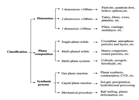
Fig (1.3) Classification of nanoparticle according to different parameter
- Nanomaterial determination
- The study of crystallographic structure, chemical composition physical properties of nano materials can be done by using X-Ray differaction [18].
- Bandgap and particle size of nanomaterial can be determined by using
UV-V is spectroscopy [18].
- Chemical composition in nanomaterials can be analyzed by using FTIR [18].
- Surface topography of nanomaterial can be scanned by using AFM, SPM [19].
- Particle size of nanomaterials can be calculated by using SEM and TEM[20].
- Properties of nanoparticles
Comparing with bulk materials the physical, chemical, optical properties of nanoparticles are different. This is due to the confinement effect [21].
- Reactivity
As particles get smaller there surface area increases that why they react differently with their environment than larger particles.
- Optical property
The smaller size of the particles have different optical properties, there is change in colour as the particles absorb and reflect light differently. For example colour range of Gold varies from purple to red depending on the size of the atom clusters [22].
- Magnetic property
Smaller particles are having different magnetic properties than the bulk particles. The spin of the electron change when reduces the size of the particles [22].
1.6 Advantages and Disadvantages of Nanoparticles
Advantages
- Rate of dissolution increased.
- Oral bioavailability increased.
- Less amount of dose require for any disease.
- Because of nano size solubility enhanced.
- Increased surface area gives high efficiency for carrying drugs.
- More rapid onset of therapeutic action.
- To affect cells and tissues nanoparticle can be used as drug delivery vehicle.
- Life times of nanoparticles are more.
- Both hydrophobic and hydrophilic substances incorporation can be possible.
- A nanoparticle reduces toxic effects [23][24]
Disadvantages
- Handling of nanoparticle either in liquid and dry form is difficult..
- Quantity of drug loading in nanoparticles is less.
- Small size nanoparticles will penetrate into skin and can cause skin cancer [25].
- Nanoparticles increases pollution in the water and air.
- Polymeric nanoparticles having less biodegradable property which will cause harmful effects in the internal part of the body [25].
- Nanotechnology is very expensive, for developing it can cost a lot of money.
- Some kinds of carbon nanotubes may cause mesothelioma.
- It can also effect the aquatic life [26][27]
1.7 Application of Nanotechnology
- Drug delivery and novel therapeutics systems.
- Diagnostics, cancer treatment and targeted drug delivery [28].
- Sport industry, cosmetics, clothing and space elevators [28].
- Nano imaging tools, analytical tools.
- It can be used in surface coating, painting and inks.
- It used in agriculture, food and beverages.
- Drastic used in pharmaceutical and natraceuticals.
- Faster processing, morphing computers and smaller more powerful mobile device.
- Cleaner energy, better energy storage.
- Treatment of water by nanoparticles.
- Solar devices made up of nanomaterial store sufficient amount of energy and more efficient than normal batteries [29][30][31].
1.8 INTRODUCTION OF CADMIUM SELENIDE NANOPARTICLES
An inorganic compound cadmium selenide is with the formula CdSe. It is classified as a 2-6 semicondutor of the n-type that is a black to red solid. Quantum confinement property exhibit by derived nanoparticles CdSe with the sizes below 10 nm. When the electrons in a material are confined to a very small volume quantum confinement comes into the picture. A CdSe quantum dot one type of CdSe nanoparticle [32]. Variation in electronic transitions result of discretization of energy states by quantum dot size. Closer electronic states in the larger quantum dots have than smaller quantum dots, to excite an electron from HOMO to the LUMO in larger quantum dot required is lower energy than the same electronic transition present in a smaller quantum dot. A red shift in absorbance spectra for nanocrystals with larger diameters this is due to quantum confinement effect.
- Formula: CdSe
- Molar mass: 191.39 grams/mole
- Melting point: 1,268 °C
- Density: 5.816 g cm−3
- Colour: Black, translucent, adamantine crystals
- IUPAC: Selanylidenecadmium

Fig(1.4) Sample of nanocrystalline cadmium selenide
CRYSTAL STRUCTURE OF CdSe
There are three types of crystalline CdSe. These are as follows:
- Wurtzite (hexagonal)
- Sphalerite (cubic)
- Rock salt(cubic)
The sphalerite CdSe structure is unstable and converts to the wurtzite form by moderate heating. At about 130 °C, and at 700 °C the transition started it completes within a day. Under high pressure the rock-salt structure is only observed [33]
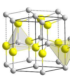
Fig (1.5) Unit cell ball stick model of cadmium selenide Wurtzite structure
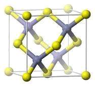
Fig (1.6) Sphalerite crystal structure of CdSe
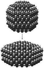
Fig (1.7) Wurtzite to rock salt structure
- PROPERTIES
- Appearance: Black, translucent, adamantine crystals.
- Odour: Odourless
- Bandgap: 1.7eV
- pH: 8-11%
- Refractive index : 2.5
- APPLICATION OF CdSe NANOPARTICLES
- In solar cell, thin films.
- In photoresistors.
- Light emitting diodes.
- Biofluorescent tagging.
- In window for instrument utilizing IR light.
- Drug delivery.
The above chapter discusses about the nanotechnology, nanoparticles, classification of nanoparticles and various synthesis processes for the preparation of nanoparticles. Various properties were also discussed which reveals the idea that the material property changes with decrease in shape and size. Also covers different issue regarding nanotechnology like advantages and disadvantages of nanoparticles. Application of nanotechnology are also discussed. CdSe nanoparticles its property, crystal structure, types synthesis technique is also mentioned. The importance of the use of cadmium selenide nanoparticle is reviewed in this chapter.
CHAPTER 2
2.1 LITERATURE REVIEW
Nanotechnology is a multidisciplinary branch includes biology, chemistry, physics, engineering and materials science. Nanotechnology actually means a technology on nanoscale that has application in the real world. Nanotechnology consists of production and application of system like physical, chemical, biological which is ranging from atoms or molecules to submicron dimensions, Also the integration of these nanoparticles or nanostructure into large systems.
At nanoscale the discovery of novel materials provides fresh opportunities for the development of innovative nanostructure materials and nanosystems. [34]
Nanotechnology concept was first discussed in 1959 by renowned physicist Richard Feynman in the session of American physical society meeting at California Institute of Technology (CalTech). In this session in his talk he gave the statement that “There’s Plenty of Room at the Bottom”, he considered that there is a possibility of direct manipulation of individual atoms for synthesis purpose. Richard P. Feynman is known as the father of nanotechnology. In 1974 nanotechnology was first time introduced in the scientific world by N. Taniguchi at the International conference in Tokyo. Idea of nanotechnology forward by Feynman were developed by E. Drexier in his book
“Vehicles of creation: the arrival of the nanotechnology era” which was published in 1986.[35] . Kroto et al. in 1965 Buckball and fullerences were discovered. In 1990, the first journal of nanotechnology was published. Feynman was awarded for his work in 1993. By 2000 President
Bill Clinton announced “U.S National Nanotechnology Initiative”. [36]
In large extent of scientific studies in the nanotechnology field includes fabrication, understanding and application of materials, devices and system at nanometer dimension. Upcoming development in nanotechnology, through which impossible will become possible that is nanomaterial with novel optical, electrical, and magnetic properties. The properties in nanometer range are strongly dependent on their size, morphology and preparative methods.
I have studied some research papers for synthesis of CdSe nanoparticle which are as follows:
Margaret A. Hines et al. in 1996 have been synthesis the ZnS-capped CdSe semiconduter by two steps single-flask method using organometallic reagents . With ZnS capping having thickness 3 Å the yield core of monodisperse CdSe of diameter 27-30 Å by X-ray photoelectron spectroscopy tool, transmission electron microscopy tool and optical absorption analysed CdSe crystals.
Bandgap of the ZnS capping is of the higher than CdSe reduce the surface reativity of the core. With a 50% quantum yield of band-edge luminescence of nanocrystals having strong and stable at room temperature. [37]
Encai Hao et al. in 1999 have been reported the microemulsion method used to synthesized nanoparticles, what are the optical properties of CdSe nanoparticles and CdSe/CdS nanoparticles which are and followed by toluene/methanol (60:1). Most notable thing in this work was yield of strong narrow band-edge luminescene by capping of CdSe with CdS. By removing surface deep trap luminescene successful passivation is obtained. Further, enhancement of the photoluminescence quantum yields of the CdSe and CdSe/CdS nanoparticles by with cadmium ions proper surface modification done. Optical spectroscopy and structural characterization was done by X-ray photoelectron spectroscopy, X-ray diffraction technique suggested the core/shell structure of CdSe/CdS samples. Elemental composition of the CdSe and CdSe/CdS nanoparticles was confirmed by X-ray photoelectron spectroscopy data. The bulk Wurtzite crystal structures of CdSe, the Peak position of CdSe and CdS in diffraction patterns corresponding to that. [38]
Andrey L. Rogach et al. in 1999 have been reported that for the preparation of II-VI semiconductor materials the wet chemical route was used, partcles are quantum in size, a series of thioglycerol-capped crystalline CdSe nanoparticles by using mercapto-alcohols(2-mercaptoethanol, 1-thioglycerol) and mercapto acids (thioglycolic acid, thiolactic acid) as stabilizers have been synthesized in aqueous solution. By using thioalcohols as capping agents smaller CdSe particles approximately 1.4-2.2 nm in diameter were obtained and by using thioacids as stabilizers larger CdSe particles of 2.1-3.2 nm in diameter were produced. Seperation of CdSe nanoparticles from the crude solutions as redissolvable powder samples by using a size-selective fractionation. Prepared samples of CdSe have been characterized by X-ray diffraction, UV-vis absorption, photoluminescence spectroscopy, and high-resolution transmission electron microscopy, and energy-dispersive X-ray analysis. By using an extended effective mass approximation a calculation of the HOMO-LUMO gap of CdSe particles as a function of their size. [39]
Frederic V. Mikulec et al. in 2000 have been studied the synthesis of II-VI semiconductor nanocrystals doped with transition metals and proved to be difficult. At high temperature pyrolysis in trioctylphosphine oxide (TOPO) CdSe quantum dots (QDs) were produced, to successfully incorporate low level of Mn specially designed precursors used. The most dopant atoms present on the surface layers of the inorganic lattice reveal by simple etching experiment and electron paramagnetic resonance (EPR) measurements. Cd magic angle spinning (MAS) nuclear magnetic resonance NMR spectra was dramatically affected by dopant. When Mn incorporated in the QDs longitudinal relaxation time decreased and paramagnetic shift observed. There was large effective magnetic fields generated by Paramagnetic atoms in QDs, by doping magnetooptical experiments can be performed. Results were found when external magnetic field is applied. fluorescence line narrowing (FLN) studies on Mn-doped CdSe QDs mirror previous findings on undoped QDs.
Junjie Zhu et al ., in 2000 have been reported that a very simple fast reaction between acetates or sulfates of Cd, Pb, and Cu and Na2SeSO3 in the presence of complexating agents nanoparticles of various dimensions of II-VI binary chalcogenides CdSe, PbSe, and Cu2-xSe, have been prepared using microwave irradiation. By X-ray diffraction (XRD), electron microscopy (TEM) and X-ray photoelectron spectroscopy (XPS) nanoparticles were analyzed. The average crystalline size was determined by the Debye-Scherrer equation. By Transmission Electron Microscopy (TEM) the morphology of the prepared nanoparticles was studied. [41]
Dmitri V et al., in 2001 have been reported highly monodisperse CdSe nanocrystals in a three-component hexadecylamine-trioctylphosphine oxide-trioctylphosphine (HDA-TOPO-TOP) mixture. Much better control over growth dynamics obtain when con-ventional organometallic synthesis of CdSe nanocrystals in TOPO-TOP. At room temperature by surface passivation with inorganic (ZnS) or organic (alkylamines) shells quantum efficiency of the band edge luminescence of CdSe nanocrystals can be improved to 40-60%.. Exchange of TOPO at the surface of CdSe nanocrystals accompanied by amines can be a slight blue shift of both the absorption spectrum edge and the maximum of the band edge PL band. [42]
Junjie Zhu et al., in 2001 have been reported the synthesis of CdSe nanoparticles by a simple reaction between CdCl2 and Na2 SeSO3 in the presence of a complexant using photoirradiation. CdSe was obtained in the cubic sphalerite phase. The synthesized nanoparticles were characterized by using diffuse reflection and photoluminescence (PL) spectrum X-ray diffraction (XRD), Transmission electronmicroscopy (TEM). According to the XRD spectrum the sizes of the as-prepared sample were calculated by the Debye–Scherrer formula which was about 7 nm. From TEM images similar result can also been obtained. The CdSe grains are spherical and monodisperse which is found by using TEM whose average grain sizes ranges from 5-8 nm. Results are in agreement with the XRD result. [43]
Baoquan Sun et al., in 2003 studied the performance of photovoltaic device fabricated from blends of branched CdSe nanoparticles as compared with devices made from nanorod/polymer blends. The improved electron extraction in photovoltaic device by using 3D CdSe tetrapod’s which improved electron transport perpendicular to the plane of the film. 1.8% Conversion efficiencies were achieved by solar power and AM1.5 illumination for a device containing 86 wt % of nanoparticles. In polymer/nanoparticle photovoltaic devices nanorods can control nanoparticle shape in 3 dimensions. The surface topography of polymer/nanorod and polymer/tetrapod films was studied by using Atomic Force Microscopy [44].
Monika BaEumle et al., in 2004 have synthesized CdSe quantum dots (QDs) with a high fluorescence quantum yield of 25% and a narrow size distribution in a single step. She used glutathione as a stabilizing molecule in water. The exceptional optical properties enabled for the first time the detection of in-water-prepared single quantum dots at room temperature. The QDs coated with streptavidin can be used as fluorescent bioanalytical probes. While preserving their capability and their optical properties to bind in addition biotinylated molecules these QDs self-assemble with high contrast on micro patterned biotin. For several months this resulting solution of QDs is stable at 4 °C. [45]
Liberato Manna et al., in 2004 have been reported the atomistic detail of the interaction between organic surfactant molecules and the surfaces of CdSe semiconductor nanoparticles. The first principles electronic structure simulations are used. The relaxed atomic geometry of organics bound to semiconductor surfaces at the nanoscale. Also the electronic charge transfer between surface atoms and the organics can be provided by this calculation. They calculate the binding energy of phosphine oxide, phosphonic and carboxylic acids and amine ligands to a range of CdSe nanoparticle facets. On the nanoparticle surface the dominant binding interaction is between cadmium atoms and oxygen atoms in the ligands. The sides of CdSe nanorods are formed by the strongly bound ligands are phosphonic acid molecules, which bind preferentially to the facets. The hypothesis that these binding energies control the relative growth rates of different facets supported by the calculated relative binding strengths of ligands to different facets, and finally the resulting geometry of the nanoparticles. [46]
M. Behboudnia et al., in 2007 have been reported synthesis of Cubic CdSe nanoparticles at room temperature (27◦C) by using cadmium acetate dihydrate (C4H6CdO4·2H2O) as a Cd2+ ion source and sodium selenosulfate (Na2SeSO3) as a Se2− ion source with the aid of ultrasound irradiation in normal laboratory conditions. The product consists of nanocrystallites of about 20nm by Scanning electron microscope (SEM) images. The nanocrystallites aggregated in the form of polydispersive nanoclusters with dimensions in the range of 150–200nm. The particles are excellently crystallized determined by X-ray diffraction analysis. The product is almost stoichiometric. The formation of purely CdSe nanoparticles and average atomic percentage of Cd to Se is about 52:48. It is characterized by dispersive X-ray spectroscopy (EDX) measrements. In prepared nanoparticles the presence of direct transition with energy band gap of about 2.02eV is obtained by UV–visible absorption spectroscopy. A blue shift of about 0.28 eV is detected and 1.74eV in correspond to its bulk value, due to confinement of electron and hole in small volume [47].
Mohammed T.Hussein et al., in 2014 have been reported by chemical reaction of sodium selenosulfide (Na2SeSO3) and cadmium chloride CdCl2 at various concentration of Selenium Se precursor preparation of II-VI Zinc-blende cadmium selenide CdSe nanoparticles as a collided can be obtained. For characterization studies of the CdSe QDs X-Ray Diffraction, UV-Visible, AFM as well as D.C conductivity are used. Zinc-blende phase of CdSe QDs shown in the X-R diffraction patterns. With decreasing QDs size which is attributed to quantum confinement affect the absorption spectra show a blue shift. The size and roughness of CdSe QDs effected which is shown in AFM measurement is due to the increasing of Cd and Se molar ratio. The results of the energy gap which had done earlier by using Density functional theory coupled with large unit cell approximation this result of the energy gap are in comparable with theoretical calculation. [48].
Kanupriya Sharma et al., in 2014 have been reported the synthesis of nanoparticles of cadmium selenide (CdSe) with cadmium acetate and sodium selenite as precursors by sonochemical method. To control the size of the nanoparticles hydrazine hydrate and ammonia were used. The particle size and crystalline nature of the samples were characterized by powder X-Ray Diffraction analysis. As the concentration of dopant increases the frequency of absorption at 890 cm-1decreases shown in FTIR results. With decreasing nanoparticle size the absorption exhibit blue-shift, which is attributed to quantum confinement effect. The dielectric constant and refractive index is dependent on absorbance. With particle size the extinction coefficient values increases. [49]
Rahul Jain et al., in 2015 have synthesised a good quality cadmium selenide nanoparticles by less hazardous and convenient route by thermolysis. In the nitrogen atmosphere at 330◦C thermolysis of a novel single source precursor, CdCl2 [Se {(CH2)2NH2}2] was done. This was result in the synthesis of nanomaterials have been characterized by X-ray powder diffraction, transmission electron microscope, scanning electron microscope and ultraviolet-visible spectroscopy,. Synthesized CdSe nanocrystals have uniqueness of Hexagonal (Wurtzite). CdSe with particle size 76nm in an average revealed by X-ray diffraction peaks . A wide energy band gap of 2.94 eV shown in electronic spectrum [50].
The above chapter defines the brief documentation of cadmium selenide nanoparticles. This paper reveals different synthesis process, characterization techniques and its analysis. Mostly chemical method is used for synthesis of cadmium selenide nano particles such as two steps method, co-precipitation method, sonochemical method microemulsion method, thermolysis convenient route. From the above process co-precipitation method is best adopted method since it is easy and cost effective. Simple fast reactions between acetates sulphate of Cd can be used. Cubic CdSe nanoparticles at room temperature formed. For the preparation of II-VI semiconductor materials of quantum size, a series of CdSe nanoparticles which are thiogylcerol-capped crystalline were formed by using wet chemical route. Hence cadmium selenide have much potential uses in the field of Nano electronic industry for semicondutor in electronic circuit, sensors. XRD, EDX, SEM, TEM and UV-VIS characterization technique are used for study properties of cadmium selenide nanoparticles. In this project co-precipitation method were used for synthesis of cadmium selenide nanoparticles is being discussed.
CHAPTER 3
3.1 PROBLEM DEFINITION
Size of CdSe nanoparticles is depend on concentration Se in the solution, so by changing the concentration of Se can obtain different size of nanoparticles Green synthesis of CdSe nanoparticle by different leaves extract and my aim is to study the variation in particle size. The obtained particle can be characterized by XRD, SEM, TEM and UV-Vis spectroscopy to study the corresponding crystal structure, morphology and absorption spectra.
CHAPTER 4
4.1 METHODOLOGY
There are various methods for synthesis of nanoparticle including bottom-up (chemical method) and top-down (physical method) which are mentioned in the figure. In my project I am using chemical process.
Fig.4.1 Top-down and bottom-up technique
A wide variety of chemical, physical and biological synthesis techniques are available for the preparation of CdSe nanoparticles but the simplest yet accurate method is the chemical method. we can also use green synthesis method for synthesis of nanoparticles which eco-friendly method, which will affect the environment. There are also various approaches which have unique properties and features for different methods.
4.2 SYNTHESIS PROCEDURE
We have synthesized CdSe nanoparticles by co-precipitation method. Take CdO and SeO2 in 2:1 ratio, 0.66gm CdO and 1.1096 gm. SeO2 in 10 ml of distilled water .This solution now put on magnetic stirrer for 2 hours. Add capping agent (Thioglycerol) in this solution. Now Ammonia is added drop wise to maintain the pH between 8-11, continuous stirring for 2 hours. Precipitate is formed; wash the percipitate with distilled water, centrifuge in centrifugation machine for 5 min. Put the sample in oven at 50°C for 3 hour. Grind the sample by using mortar and then put sample in muffle furnace at 400°C for calcination. For characterization UV, XRD and optical microscopic image were taken.
(a)Chemicals required
- Cadmium oxide
- Selenium dioxide
- Thioglycerol
- Distilled water
- Ammonia
(b) Equipments
- Weighing machine
- Magnetic stirrer
- Heating plate
- Hot air oven
- Muffle furnace
- Centrifugation Machine

Fig.4.2 Hot Air Oven (Source: Medicaps University, Environment Lab)


.

Fig.4.3 Analytical Weighing Machine Fig.4.4 Magnetic Stirrer
(Source: Medicaps University, Environment Lab) (Source: Medicaps University,
Environment Lab)

Fig.4.5 MuffleFurnace
(Source: Medicaps University, Environment Lab)
4.3 FLOW CHART
Start

Take CdO and Seo2 in 2:1 ratio, 0.66gm CdO and 1.1096 gm Seo2 in 10 ml of distilled water

Put on magnetic stirrer
Add capping agent (ThioGlycerol)

Ammonia is added drop wise to adjust PH between 8-11

Continuous stirring for 2 hours
Precipitate is formed, centrifuge in centrifugation machine for 5 min.

Put sample in oven at 50 °C for 3 hour
Grind the sample by mortar & then put sample in muffle furnace at 400 °C

Take UV of CdSe sample particle

End
Fig.4.6 Flow chart of Cadmium selenide by using CdO and SeO2
4.4 CHARACTERIZATION TECHNIQUE
The resultant sample can be characterized by different methods, such as XRD, TEM, SEM, XPS, FTIR, DTA, DSC, UV-Vis spectroscopy and optical microscopy etc. From this some are as follows:
4.4.1 X-ray diffraction (XRD)
As the X-Rays scattered by crystals Bragg’s law was used to explain the interference pattern of X-Rays, For all the states of matter to study the structure of it diffraction has been developed, with a wavelength value of any beam (ie; ions, electrons, neutrons, and protons)similar to the distance between the atomic or molecular structures of interest. The Bragg’s were awarded the Nobel Prize in physics for their work in 1915 for determining crystal structures beginning with NaCl, ZnS and diamond.
For characterization of different crystalline solids the X-ray diffraction technique is an analytical technique which is most extensively used. In X-rays diffracted the position and intensities of by a crystalline solid provide a lot of information such as crystal structure, composition of the solid, average particle size, unit cell dimensions and purity of the prepared sample. X-rays which are used here are in the form of electromagnetic radiation of very short wavelength and they are produced when high speed electrons are stopped by a solid object. Whenever high-speed electrons collide with a metal target X-rays are produced. Hot W filament is a electrons source ; between the cathode (W), the anode and a metal target, Cu, Al, Mo, and Mg keeped a high accelerating voltage. Desired target metal contained in the block made up of Cu the anode is a water-cooled block. In this crystal different atoms and molecules are organised in different planes in a systematic and repetitive manner. These inter-planar distances in the crystal are of the same order in magnitude of the wavelength of the characteristic X-rays emitted by the target. A diffraction grating to the X-rays act by the crystal planes and diffraction occurs. For X-ray diffraction to occur the necessary condition is represented by Bragg’s equation.
nλ = 2d sin θ
Where,
n is an integer (1, 2, 3, etc) called the order of reflection
θ is the glancing angle of incident X-ray beams on the crystal surface d is the inter-planar spacing
- is the wavelength of X-rays
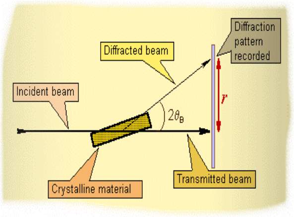
Fig 4.7 Block diagram of XRD
4.4.2 Scanning Electron Microscopy (SEM)
At microscopic levels the Scanning Electron Microscope is used to study the samples. Electron image of specimen’s surface produced by the instrument is of resolution better than 100Å. The technique is used for the investigation of size, shape and surface texture. In Scanning electron microscopy (SEM), the electron beam does not pass through the specimen rather it interacts with the specimen surface and results in reflection of low energy secondary electrons from it which takes part in image formation. The morphology of the samples was studied by SEM
4.4.3 X-ray Photoelectron spectroscopy (XPS)
A very important technique X-ray Photoelectron Spectroscopy (XPS) also known as ESCA (Electron Spectroscopy for Chemical Analysis) for determining the atomic and molecular energy levels and hence the ionization energies of atoms and molecules. Before analysis the sample surfaces were scraped. To get the right carbon peak position verified measurement conditions and parameters.
4.4.4 Fourier Transform Infrared (FTIR) Spectroscopy
For analysing samples infrared spectroscopy is a valuable tool. Infra-red spectrum region lies between 4000-400cm-1. Energy changes arising as a consequence of molecular vibrations of the bond stretching and bending type results in absorption bands in the spectrum. For identifying the organic ligands bound to the metal ion, metal oxygen bonds as well as the adsorbed species on the catalysts surface it has been widely used. In the place of monochromator the non-dispersive type of IR instrument has an interferometer and the instrument is called as Fourier Transform Infra-red Spectroscopy (FTIR).
The different components of FTIR are:
- Source
- Michelson Interferometer
- Sample compartment
- Detector
IR spectra of the metal precursors and their decomposed products were recorded by FTIR instrument.
4.4.5 Differential Thermal Analysis (DTA)
With the energy changes Differential Thermal analysis (DTA) is one of the oldest and simplest thermal techniques used for the study of physical and chemical transformations in materials associated. At the predetermined constant heating rate in the controlled atmosphere the temperature difference between the sample and the thermally inert reference is measured when both are heated simultaneously in DTA temperature/time keeping as a function.
4.4.6 Differential Scanning Calorimetry (DSC)
Differential Scanning Calorimetry (DSC) analysis provides the differential heat flux between the sample which is obtained and reference material which we are taking temperature keeping as a function. Basically DSC depends on temperature. The different components of a DSC instrument are:
- Sample and reference container
- Average temperature amplifier
- Differential temperature amplifier
- Programmer
The above chapter, we have discussed the various synthesis methods of nanoparticles bottom up and top down approaches. Synthesis procedure of cadmium selenide by using co-precipitation method, what are the chemical and equipment needed are discussed. Chemical procedure follow is explained by flow chart. Described the different techniques which can be used for characterization like XRD, DTA, DSC, FTIR, XPS, SEM.
CHAPTER 5
RESULT AND DISCUSSION
5.1 Characterization of CdSe nanoparticles using Optical Microscope
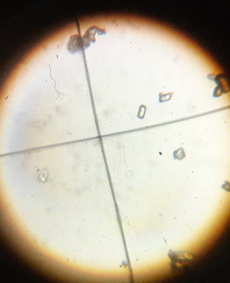
The synthesized CdSe nanoparticles were analysed by optical microscope and following images observed as a result.
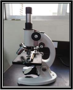
Fig.5.1 Optical Microscope (Source: Medicaps University, Nanotechnology Lab)
 .
.
Fig.5.2 CdSe nanoparticles shown in Optical Microscope (Source: Medicaps University, Nanotechnology Lab)
5.2 Characterization using X-RAY Diffraction
In any compounds XRD is the easiest characterization tools to determine the size as well as the shape of the unit cell in material science and solid state chemistry [51]. With the help of XRD we can measure the average spacing between row and layers of the atoms. Orientation of a single crystal structure or grain can be determined by XRD [52]. Unknown material crystal structure can be found out. In the small crystalline regions with XRD we can measure the size, manipulate weather the sample is pure or not. Lattice parameter determination and phase fraction analysis is quantitative analysis and phase identification is qualitative analysis for both analysis Powder Diffraction Method is useful [53][54]. To measure various structural properties of the crystalline phases such as grain sizes, phase compositions, strain and defects structures can be easily obtain by XRD characterization.
Principle: X – Rays with suitable wavelengths results in inelastic and elastic scattering of the radiation when there is the interaction between matter and X-Ray. The observed diffraction of the incident X-Ray beam by the sample is the elastic scattering from the electrons inside the matter. When X-Ray incident on the crystal atomic plane present in the crystal cause an incident X-Ray beam to interfere with one another as they leave the crystal the phenomenon is called X-Ray diffraction. It follows Bragg’s Law.
Bragg’s Law: With identical wavelength and phase of two beam of X-Ray reaches a crystalline solid and are scattered by two different atoms within it Bragg’s diffraction occurs. Extra length 2dsinϴ by the lower beam traverses. When this length is equal to an integer multiple of the wavelength of the radiation which coming then only constructive interference occurs [55].
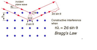
Fig 5.3 Bragg’s law
Where n = 1, 2, 3, …………….
λ = wavelength
d h k l = distance between adjacent planes of atom indexed as h k l
The condition n λ = 2dhklsinϴ.
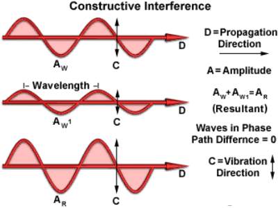
Fig 5.4 Constructive interference (In phase)
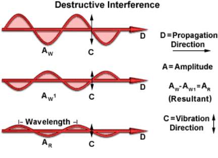
Fig 5.5 Destructive interference (Out of phase)
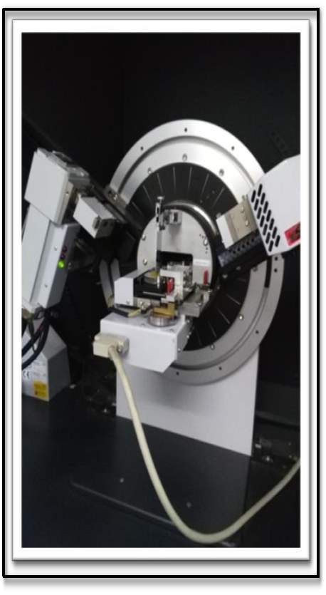 In my work XRD characterization techniques is used to determine the characteristics of prepared CdSe nanoparticles. In UGC-DAE consortium for Scientific Research Indore the facilities for characterization of the samples are available. In the XRD laboratory Bruker D8 Advance XRD was installed in June 2010. This XRD is equipped X-ray source of CU-Kα with 3kW x-ray generated and goniometer with step size of 0.0001°. For characterization of samples there are 9 sample holders in series present in this Bruker D8 Advance XRD [56].
Fig.5.4 XRD Apparatus
Fig.5.6 XRD Apparatus
(Source: UGC-DAVV, Indore)
Prepared CdSe nanoparticles X-Ray powder diffraction analyses are shown in tabulated form (Table 1). By using Scherrer’s formula crystalline size are calculated and by comparing the obtained 2θ with corresponding Joint Committee for Powder Diffraction Studies (JCPDS) data No.77-2307 crystal structure determine [57].
Table 1 Miller indices of Cadmium Selenide at different peak
| 2ϴ | ϴ | Sin2ϴ | h2+k2+l2 | hkl | |
| 25.3361° | 12.6680° | 0.04809 | 4 | (002) | |
| 27.1345° | 13.5672° | 0.05504 | 2 | (101) | |
| 35.1772° | 17.588° | 0.09132 | 5 | (102) | |
| 45.8176° | 22.90° | 0.15156 | 10 | (103) | |
| 55.8585° | 27.9292° | 0.2194 | 8 | (202) | |
| 67.8477° | 33.9238° | 0.3114 | 6 | (211) | |
| 69.0965° | 34.548° | 0.3210 | 18 | (114) | |
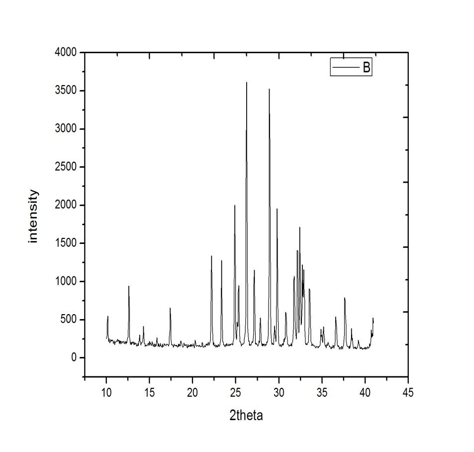 Fig 5.7 XRD Graph of Cadmium Selenide Nanoparticles
The structure of cadmium selenide nanoparticles was analyzed by X-Ray diffraction technique; the 2Ɵ and intensity were obtained. The graph 2Ɵ verses intensity has been plotted as shown in Fig 5.5. With reference data obtained 2Ɵ peaks has been compared. In the comparison it was found that JCPDS NO.77-2307 which has been matching with obtained. Thus the obtained nanoparticles are formed in the Hexagonal (Wurtzite) CdSe nanoparticles due to presence of other diiferent kind of phase in the sample we can observed some additional peaks in the XRD pattern. CdSe in the pure form and single phase has not been successfully obtained under the present conditions [58].
Peak Indexing: Indexing process is used to determine the dimensions of unit cell from the peak positions. Fig 5.5 shows the XRD graph of Cadmium Selenide nanoparticles. Indexing process is first step in diffraction pattern analysis. It is necessary to assign Miller Indices (h k l) to each peak of the graph to index a powder diffraction pattern. Form the range of 10° to 80 ° the data was taken with a step of 0.0001°. Seven peaks at 2ϴ values of 25.3361°, 27.1345°, 35.1772°, 45.8176°, 55.8585°, 67.8477°, 69.0965° corresponding to (002), (101), (102), (103), (202), (211), (114) planes of cadmium selenide were observed. We calculate “d” at wavelength 1.5 Å by using Bragg’s law
n λ = 2dhkl sinϴ
Table 2 Interplaner distance at different peaks
| 2ϴ | ϴ | Sinϴ | hkl | d (Å) |
| 25.3361° | 12.6680° | 0.2193 | (002) | 3.5123 |
| 27.1345° | 13.5672° | 0.2346 | (101) | 3.2832 |
| 35.1772° | 17.588° | 0.3022 | (102) | 2.5488 |
| 45.8176° | 22.90° | 0.3893 | (103) | 1.9785 |
| 55.8585° | 27.9292° | 0.4684 | (202) | 1.6444 |
| 67.8477° | 33.9238° | 0.5581 | (211) | 1.3801 |
| 69.0965° | 34.548° | 0.5671 | (114) | 1.3582 |
Particle Size Calculation
The peak at several degrees from this study considering, By using Debye-Scherrer formula
the average particle size has been Calculated
Debye-Scherrer formula
Paul F. Fewster “A new theory for X-ray diffraction” Acta Crystallogr A FoundAdvPMC4011009.
53 Jan Drenth “Theory of X-ray Diffraction by a Crysta”DOI 10.1007/0-387-33746-6_4 Springer New York.
54 https://en.wikipedia.org/wiki/X-ray_crystallography.
55 Bragg, W.H.; Bragg, W.L. (1913). “The Reflexion of X-rays by Crystals”. Proc R. Soc. Lond.A. 88 (605):42838. Bibcode:1913RSPSA..88..428B. doi:10.1098/rspa.1913.0040.
56 B. Fultz “Chapter 1 Diffraction and the X-Ray Powder Diffractometer” Springer-Verlag Berlin Heidelberg 2013.
57 Pdf 77.2307 JCPDS:- Stevenson. A.W., Barneaz, Acta crystallogr., Sec.B: Structure science 40, 530,1984.
58 Pdf 190.191 JCPDS:- Stevenson. A.W., Barneaz, Acta crystallogr., Sec.B: Structure science 40, 530,1988.
Cite This Work
To export a reference to this article please select a referencing stye below:
Related Services
View all


Related Content
All TagsContent relating to: "Earth Sciences"
Earth Sciences is a field of study that focuses on the science behind planet Earth. Earth Sciences explores the physical and chemical aspects of not only planet Earth, but it's atmosphere too.
Related Articles

DMCA / Removal Request
If you are the original writer of this dissertation and no longer wish to have your work published on the UKDiss.com website then please: