Mobile Gait Analysis System
Info: 14119 words (56 pages) Dissertation
Published: 11th Dec 2019
Tagged: Medical Technology
Chapter 4 Results and Discussion
Chapter 5 Conclusions and Recommendations
Appendix B Salient Extracts from Project Diary
Appendix C Design Drawings & Component Specifications
Appendix D List of Software Code
Appendix F Other Technical or Data Appendices
RAM Random Access Memory
PC Personal Computer
Figure 1 System Overview……………………………………………1
Figure 2 Sub-system Overview………………………………………..2
Table 1 Experiment Trials……………………………………………1
Table 2 Experiment Results…………………………………………..2
Chapter 1 Introduction
1.1 Problem
As we understand the mechanics of our body, we have started to realize that correct biomechanical movement is extremely important. Biomechanical movement means the movement of the muscles and bones when our body parts move. If incorrect biomechanical movement is detected at early stages, it can reduce the risk of an injury. Even if when an injury does occur, the process of recovery can be shortened and the problem can be reduced or eliminated by identifying the problem that caused the injury in the first place.
Gait analysis is one tool that can be used to identify and reduce the risk of repetitive type injuries which can be caused by sports, the ageing process and poor health.
This project aims to make a system which will capture the walking patterns of an individual and will analyze the foot pressure data to give meaningful information to the user. This information would allow the user to give attention towards correct postures and biomechanical movement to prevent injuries and also to recover faster from an injury if it has occurred.
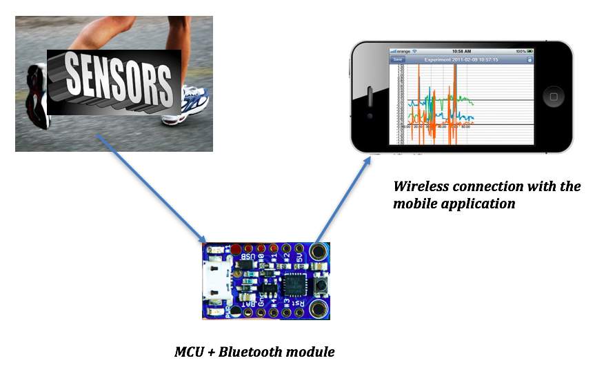
Figure 1 – Mobile Gait Analysis System
Feet offer the primary surface of interaction with the surroundings throughout locomotion. Thus, it’s necessary to diagnose foot issues at an early stage for injury prevention, risk management and general welfare. One approach to measuring foot health, widely employed in numerous applications, is examining foot pressure characteristics. It is, therefore, vital that correct and reliable foot pressure measuring systems are developed. Mueller (Mueller, 1999) observed foot pressure applied by individuals without impairments (i.e., the general public).
Considering applications involving illness identification, several researchers have targeted on foot ulceration issues as a result of diabetes that may lead to excessive foot pressures in specific areas beneath the foot.
In-shoe foot switches and area pressure devices are developed to measure gait events and foot pressure and provide a sensible means of analysis of walking performance in individuals with gait disorders.
Textile-based sensing element technology showed encouraging results on the development of foot sensors to measure gait performance (Kunigunde Cherenack, 2012). For clinical use measurements should be reliable showing repeatable measurements with none intervention. Unfortunately, literature on textile based sensing element lack repeatability studies involving gait tasks.
Major limitations among the offered pressure sensing shoe insoles within the market include: 1) devices don’t support long-term (>24 hours) information recording, and 2) shoes must be worn, which isn’t compatible to indoor daily use.
This project aimed to build a similar system which could take the foot pressure as an input and analyse that data and give meaningful information to the user.
The specific objectives of this project are:
- Building a shoe insole which would take the foot pressure data – This consists of sensors sensing the foot pressure, a microprocessor which would send this data to a Bluetooth module connected to it.
- Programming the Bluetooth module connected to the microprocessor to send data to user’s phone Bluetooth module.
- Make a mobile application to display that data to the user.
The system should be as small as possible, so that it is easy to use and portable. The data should be collected with good accuracy. The system should durable as it might be used daily by the user.
Initially analysis of data over the cloud was also considered, but due to time constraints, the idea had to be dropped.
Here you are to give your reader a guided tour of the remainder of the document. It should be more than just a list of the upcoming chapters. You should effectively overview the background, methods, and results of your report in two or three paragraphs.
- Walking Analysis – The gait cycle is also called the walking cycle. The gait cycle consists of the stance phase (i.e. when the foot is on the ground) and the swing phase (i.e. when the foot is off the ground).
The stance phase takes up 62% of the full gait cycle and the swing phase takes up the remaining 38% of one full gait cycle. These phases of gait can be seen in figure 1.
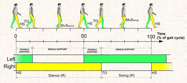
Figure 2 – Walking Phases (Gait Cycle)
As shown in figure 2, The stance phase of gait can be divided into two three parts: First, the point of initial contact of the foot on to the ground, which is also called heel strike (HS); Second, when the full foot is on the ground also called mid stance; Third, when the stance phase ends (also called toe off, TO).
While walking, there is a single-support phase (i.e. when one foot is on the ground), and a double-support phase (i.e. when both the feet are on the ground). The single-support phase starts when toe of one foot is lifted off the ground and the double-support phase starts when the same foot touches the ground. The time for which the single-support phase last is four times more than that of the double-support phase. (Bartlett)
It was necessary to understand the walking cycle phases so as to be able to analyse and understand the requirements for the project.
After understanding the walking cycle, a study was read (Hongsheng Zhu, 1991) in which, seven pressure points were taken on each foot to see where most of the pressure is applied on the foot when a person walks. This helped in understanding the positioning and number of sensors to be used. Figure 3 shows the placement of the sensors according to the study (Hongsheng Zhu, 1991).
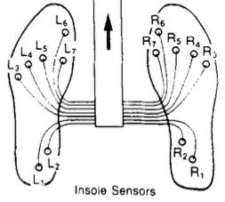
Figure 3 – Insole sensors positioning
According to figure 3, L1 to L7 are the pressure sensors on the left foot insole and R1 to R7 are the pressure sensors on the right foot insole. The data collected by these sensors was sent to a microcontroller for further analysis. The subject for this tudy were individuals with normal walking patterns (i.e. no disability of any sort).
Figure 4, shows the result of the study, showing the pressure applied on each sensor by each foot (Hongsheng Zhu, 1991). The sensor locations mentions are from L1 to L7 for left foot values and R1 to R7 for right foot values.
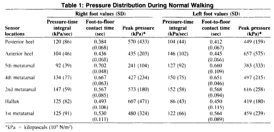
Figure 4 – Pressure Distribution during normal walking
Figure 4 clearly shows that in case of the right foot, most pressure is applied at the 2nd metatarsal (where R5 was placed) and least is applied at the 5th metatarsal (where R3 was placed). In case of the left foot also, most pressure is applied at the 2nd metatarsal (where L5 was placed), but for the least pressure applied, the sensor location was the Hallux (where L6 was placed).
This study really helped in understanding where most of the pressure is applied while walking, and where would it be ideal to place the sensors.
- Making the block diagram – After understanding the walking patterns, the block diagram was made.
The first step in making any device is to understand what goes in as input and what is expected to come as output. To get this understanding the block diagram of the system was made. This was an iterative process. Figure 5 shows the first iteration of the block diagram.
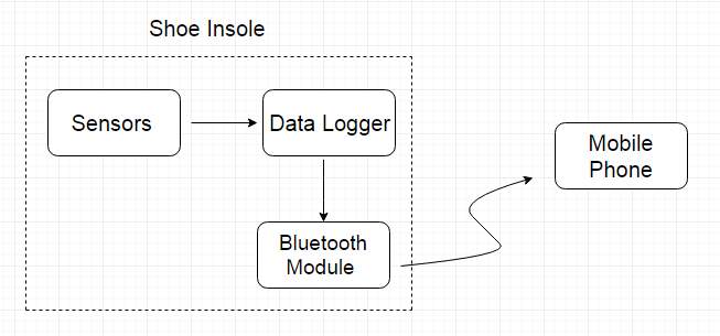
Figure 5 – Block Diagram iteration 1
As we can see in figure 5, the shoe insole comprises of sensors, the data logger and the Bluetooth module. The sensors data is being sent to the data logger, which stores it and then sends it to the Bluetooth module. This Bluetooth module then sends it to the Bluetooth of the mobile phone. As, the main aim was to send data to the phone, the data logger was removed from the diagram. The second iteration (i.e. without the data logger) is shown in figure 6.
In figure 6, the data logger is replaced by a simple microprocessor, which would receive the data from the sensors and send data to the Bluetooth module. Data loggers are generally bigger in size than microprocessors, so this helped to make the circuit smaller. This diagram (shown in figure 6) was finalized for further study and research on the components.
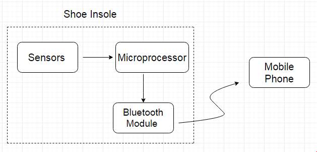
Figure 6 – Block Diagram iteration 2
The Block diagram in figure 6 fully matched all the objectives to be fulfilled, therefore, it was chosen to be the final block diagram. The next section of the report discusses which components were selected as being the most suitable for the project.
- Deciding the parts
This section is divided into three parts – selecting the sensors, selecting the microprocessor and selecting the Bluetooth module.
- Selecting the sensors – For this project, the type of sensor required was the one which would be able to get into the shoe and be comfortable to the user. Mainly three ways to take the muscle movement were considered.
The three techniques were:
1) Using Force Sensitive Resistor (FSR) sensors – These sensors are widely used for pressure (or force sensing). The output of these sensors is resistance and it varies ad pressure is applied to them. More pressure, less resistance, i.e. the resistance has an inverse relationship with the pressure applied. Figure 7 shows the FSR sensor used for this project.
2) Using textile sensors – The word “textile” itself signifies that in this method, conducting threads (or yarn) are used. These threads sense the muscle movement. They are much more comfortable to wear than FSR sensors, but its not very easy to take output from them. Figure 8 shows a textile sensor. (Perner-Wilson, n.d.)
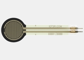
Figure 7 – Force Sensitive Resistor (FSR) sensor
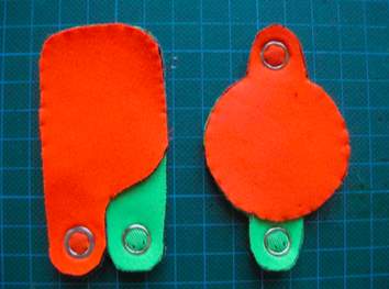
Figure 8 – Conductive thread pressure sensor
3) Using Electromyography (EMG) – Surface EMG variant of EMG techniques, tracks the functioning of the muscle by recording its activity from the skin surface above the muscles. It is generally used in medical equipments. Figure 9 shows an implementation of EMG.
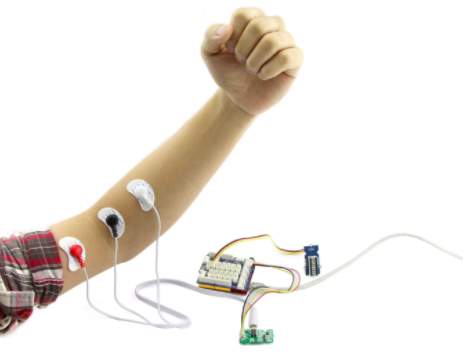
Figure 9 – Electromyography
Table 1 below compares these three techniques.
| Comparison between different muscle movement sensing techniques | ||
| FSR sensors | EMG technique | Textile Sensors |
| It varies its resistance based on the amount of pressure or force applied to it. (Ada, n.d.) | Surface EMG variant of EMG techniques, evaluates the functioning of the muscle by recording its activity from the skin surface above the muscle.
(Anon., n.d.) |
Use of conducting threads to sense muscle movement (Kunigunde Cherenack, 2012) |
| Easily Available | Needs surface electrodes | Has to be made (woven) before use |
| Easy to use (can be easily connected to a microcontroller) | Easy to connect to a computer to see muscle movement. | Complicated to connect to a microcontroller |
| Can be put into the shoe easily | Relatively difficult to put in shoe as compared to FSR. | The whole sole had to woven to put into shoe. |
| Easy to take output | Easy to take output | Because of so many woven threads, difficult to take output. |
| Easier to wear | Not very easy to wear | Easiest to wear |
Table 1 – Difference between EMG, FSR and Textile sensor techniques
After comparing the three types of sensor techniques, being the most convenient, easy to use and easily available sensor, FSR sensor was chosen for the project.
- Selecting the microprocessor – For this project a small microcontroller was required. It had to be portable and small enough to fit into the person’s shoe (or small enough to be carried in a small box). A number of microcontrollers were considered. They are as follows:
- Arduino Zero – It is a powerful board with a 32-bit microcontroller (ATSAMD21G18), which provides increased performance than other Arduino boards. It runs at 3.3 V, and has 6 Analog pins. The size of the board is 68mm by 30 mm (which makes the length equal to 6.8 cm and width equal to 3.0 cm). The size was small as compared to other Arduino boards, but due to unavailability of at least 7 analog pins, this board could not be used. (Arduino ZERO & Genuino ZERO, n.d.)
- Arduino Micro – It is a board with a different microcontroller than Arduino Zero (ATmega32U4). It has 12 analog input pins. It operates at 5v and has a size of 4.8cm by 1.8cm. Being a small and powerful board it was considered for the project. It will be compared with other boards later in the report. (Arduino MICRO & Genuino MICRO, n.d.)
- Teensy 3.2 –It is a small development board loaded with features. It has a 32-bit Cortex-M4 microcontroller and 14 analog pins. It was considered earlier but due to very less documentation and help material, it was not used in the project. (Teensy 3.2, n.d.)
- Bleduino – This board was a suitable match for the project. It has 9 analog pins having size 2.3 cm by 4.3 cm. It will be compared with other suitable boards for the project later in the report. ($34 BLEduino Bluetooth 4.0 Low Energy Arduino-Compatible Board, n.d.) (BLEduino, n.d.)
During further research, “Bluetooth Low Energy Digital Pedometer Demo Design” (Zhang Feng, Microchip Technologies, n.d.) by microchip was also studied. Figure 10 shows the pedometer demo.
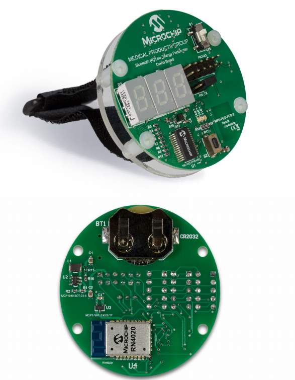
Figure 10 – Bluetooth Low Energy Digital Pedometer Demo Design
It uses the cost efficient microcontroller, PIC16LF1718, of the PIC microcontrollers family. This microcontroller is also extremely low power. It also uses the microchip RN4020 Bluetooth Low Energy (BLE) module. The Bosch Sensortec BMA250E accelerometer is also a part of the device. This accelerometer counts the steps of the user and displays it on the seven segment displays. The device can be worn on the wrist like a watch. RN4020 BLE module allows the device to send the data to another device on which the user can keep a track of his/her progress. The device gets its power from a 3V coin battery (CR2032).
All the components were studied in detail. This detailed study is included in Appendix 1.
The device was very helpful and could be used by replacing some components with other, and by wearing (strapping it) near the ankle. Unfortunately, it was not available for purchase. However, it gave another idea of using the PIC microcontrollers.
- Picaxe 18M2 – The microcontroller used in the pedometer device described above was PIC16LF1718. Picaxe produces the surface mount versions of all the PIC microcontrollers. PICAXE 18M2 was found to be the surface mount version of PIC16LF1718.
- PICAXE chips are very cost effective and are easy to program using simple, easy to understand software. All the latest PICAXE chips can be run at 3V, 4.5V or 5V. Some of the PICAXE chips can even run at 1.8V (which makes these chips extremely low power).
The PIC microcontroller, PIC16LF1718 (the surface mount version of it being PICAXE 18M2) was also considered to be a suitable choice for the system. PIC16LF1718 is compared with BLEduino in table 2.
| Comparison between PIC16LF1718 (with RN4020) and BLEduino
|
||
| PIC16LF1718 with RN4020
|
BLEduino | Arduino Micro |
| 10 Analog Pins | 9 Analog Pins | 12 Analog pins |
| Operating current – 8 micro amps to 32 micro amps | Operating current – 40 milliamps | Operating current – 29 milliamps |
| Range – up to 100 meters | Range – 100 to 300 feet | – |
| Programmed using C programming language | Arduino Programming language used to program | Arduino Programming language used to program |
Table 2 – Comparison between PIC16LF1718 (with RN4020), BLEduino and Arduino Micro
It is evident from table 2, that PIC16LF1718 draws much less current as compared to BLEduino. Therefore, PICAXE 18M2 (surface mount version of PIC16LF1718) was chosen to fulfill the projects objectives.
- Selecting the Bluetooth module – For this project, a small and extremely low power Bluetooth module was required. First, it had to be decided which technology to be used for sending the data wirelessly. Two technologies were considered, one was Bluetooth and the other was Zigbee. The comparison of both the technologies is shown in table 3 (GreenPeak Technologies, n.d.) (LinkLabs, 2015).
| Comparison between Zigbee and BLE | |
| Zigbee | BLE |
| Uses 2.4 GHz ISM frequency band | Uses 2.4 GHz ISM frequency band |
| Range approx. 291m | Range approx. 100m |
| Uses mesh topology to support unlimited number of nodes | Star topology followed supporting connection to limited number of nodes. |
| Transmitting power – approx. 18 dBm | Transmitting power – approx. 4 dBm |
| A ZigBee can only communicate with another ZigBee | Bluetooth can easily communicate with any Bluetooth device (including smartphones, laptops having Bluetooth etc.) |
| Low power consumption | Lower power consumption as compared to Zigbee |
Table 3 – Comparison between ZigBee and BLE
Although Zigbee has a better range as compared to BLE, but it is necessary to use zigbees to communicate with each other. So, if Zigbee has to be considered than one zigbee would be used in the PCB and the other zigbee had to be connected to the computer. Also the power consumption of BLE is much less as compared to zigbee. Therefore, BLE was considered to be a better choice for the project.
RN4020 was the latest, low power, small in size and easy to use BLE module (Microchip, n.d.). It has an on board embedded BLE stack, and is only 1.1 cms by 1.9 cms. It has a range of over 100 meters. Castellated SMD pads make it easy to mount on the PCB. With all these wonderful features, it was a great choice for the project.
As both PICAXE 18M2 and RN4020 were surface mount, it was decided that a PCB would be design to put all the parts together. This gave an opportunity to design the PCB as small as possible and only put the necessary components.
Summarizing this section in the following points:
1. FSR sensors were found to be a suitable for taking the foot pressure data.
2. PICAXE 18M2 was selected to be the microcontroller to which the FSR sensors would send the data.
3. RN4020 BLE module was chosen to take the data as input from the microcontroller and send it to the mobile phone (to an android application).
4. A 3V coin battery Panasonic CR2032 was chosen to power PICAXE 18M2, RN4020 and the FSR sensors.
A more detailed block diagram of the system is as follows:
Mobile Phone
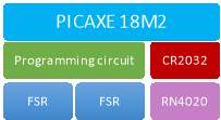
Figure 11 – Detailed Block Diagram
After finalizing the detailed block diagram, the making of the schematic diagram was considered. For making the schematic diagram, it was important to first study how the different parts of the PCB would be connected to each other (i.e. how many pins of a components would be connected to the other component; how will they be connected? etc.). To carry out this study, it was necessary to first understand the connection of the different parts are connected to the microcontroller itself.
The following sections discuss some important connection in details.
- Connection with the FSR sensors
As discussed earlier, the FSR sensors were found to be the most suitable for the project. The next step was to study their connection with the microcontroller. The connection of the FSR with the Arduino was studied. (Ada, n.d.)
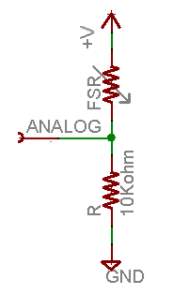
Figure 12 – Connection of FSR sensor with Analog pin of Arduino (Ada, n.d.)
Considering figure 12, say the +V is a 3V supply, the analog voltage (output value) can range from anything from 0V (voltage from ground) to 3V (from +V). It works something like this; First the resistance of the FSR sensor in infinite (when no force is applied). The resistance of the FSR sensor decreases as force is applied on the surface of the FSR sensor. This leads to decrease in the total resistance of the FSR sensor and pull down resistor (As they are in series). This causes current flowing through both the resistors to increase.
Now, the circuit shown in figure 12 is a voltage divider circuit.
Therefore, Analog voltage can be calculated as,
Vo=Rn × VccRtotal
where, Vo is the output analog voltage, Rn is the resistor across which the voltage drop has to be calculated, Vcc is the supply voltage and Rtotal is the total resistance (i.e. FSR + R). The ratio of Rn to Rtotal is equal to the ratio of Vo to Vcc. This formula (given above) is known as the voltage divider formula and it is an easier way of computing the voltage drop in a series circuit without calculating currents using the Ohms law. (All about circuits, n.d.)
To select a suitable value of R (the pulldown resistor, also equal to Rn), different values of R (=Rn) were tried. Table 4 shows the results.
| Rn (x 103 Ohms) | FSR (x 103 Ohms) | Vcc (volts) | Vo (volts) |
| 4.7 | 200 | 3 | 0.06 |
| 4.7 | 6 | 3 | 1.13 |
| 10 | 200 | 3 | 0.14 |
| 10 | 6 | 3 | 2.03 |
Table 4 – Selecting a suitable value for the pull down resistor (R)
Many values for R were tried, but only a few iterations are shown in table 4. The value of FSR is equal to 200KOhms for the case when the FSR sensor is lightly pressed (sample high resistance), and its equal to 6KOhms when it is firmly pressed (sample low resistance). The value of Vcc is set equal to 3V for all the cases, as both PICAXE 18M2 and RN4020 are powered by CR2032 (which is a 3V coin battery).
The value of Vo is calculated using the voltage divider formula. It is can be seen in table 4 that using a value of Rn equal to 4.7 KOhms gives a range of Vo to be from 0.06V to 1.13V. On the other hand, when Rn equal to 10 KOhms, Vo ranges from 0.14V to 2.03V.
As using a value of Rn equal to 10 KOhms gives a better range of Vo values, Rn equal to 10 KOhms was chosen.
As all the FSRs had to be connected to a resistor R of 10 KOhms, it was preferred to use a resistor network (also called a resistor pack). A resistor network contains more than 1 resistor of the same (or may be different) resistances (shown in Figure 13). They can be arranged in many topologies, i.e. bus, isolated etc (Bourns).
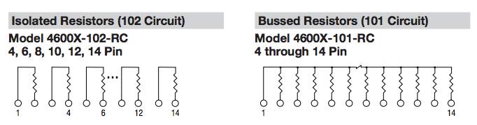
Figure 13 – Resistor Networks (Bourns)
In case of isolated resistor networks, all the resistors are isolated (separate). They do not share any common pin. On the other hand, the bussed resistor networks have 1 separate connection for each resistor and 1 common bus connecting all the resistors to the same point. For the project, bussed resistor network for found to be more appropriate. The common pin was grounded and the other each resistor was in series with an FSR sensor (as discussed earlier).
After this study, the connection of FSR with the PICAXE 18M2 was understood. The connection of FSR to the specific pins of PICAXE 18M2 will be discussed later.
- Circuit for Programming PICAXE 18M2
The manual provided by PICAXE itself was extremely helpful for designing the circuit to program the microcontroller (PICAXE). This circuit is shown in figure 13 below.
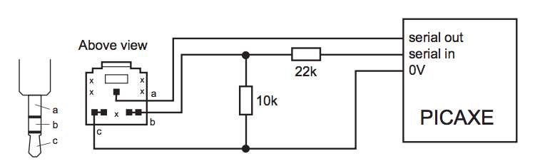
Figure 14 – Download Circuit for all PICAXE chips
The download circuit (i.e. the circuit for programming the chip) is same for all PICAXE chips. It has a connection through 3 wires from PICAXE to the AXE027 USB cable (shown on the left side in the figure). The first wire which connect point ‘a’ of the USB cable to the serial out of PICAXE is used to transmit serial output of PICAXE to the computer. The second wire which connects point ‘b’ of USB to serial in of PICAXE is used by PICAXE to take serial input from the computer. The third wire (connected to 0V) is to provide a common ground.
The two resistors used in the above circuit do not act as potential dividers. The 22k resistance works with the inner microcontroller diodes to clamp the serial voltage to the PICAXE supply voltage and to limit the download current to a suitable limit. The 10k resistance stops the serial input ‘floating’ while the download cable isn’t connected. This is essential for reliable operation.
The two download resistors should be included on each PICAXE circuit (i.e. not designed into the cable). The serial input mustn’t ever be left unconnected. If it’s left unconnected the serial input can ‘float’ high or low and can cause unreliable operation, because the PICAXE chip can receive floating signals that it might interpret as a new download attempt.
After understanding this connection, the connection of RN4020 with the microcontroller was studied. This study is highlighted in the next section.
- Connecting the RN4020 BLE module
To figure out which pins of the BLE would be connected to the microcontroller, the manual for the RN4020 had to be studied in detail (Microchip, 2014). Figure 14 shows the pinout of RN4020.
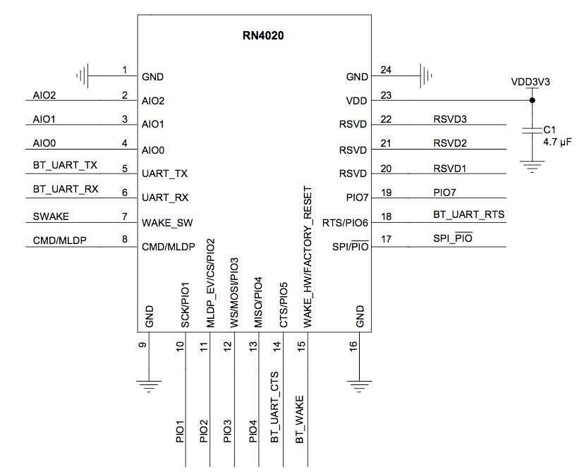
Figure 15 – Pin diagram RN4020
The pin diagram was studied in detail. The functions of some of the pins/commands are as follows:
- The RN4020 module uses the WAKE_SW (pin 7), CMD/MLDP (pin 8), WAKE_HW (pin 15) pins to switch its states
- WAKE_SW is used for controlling the current operating state of the RN4020. When WAKE_SW is high, the module wakes up and is in the Active mode. When the module is awake, “CMD” pin (i.e. pin 8) outputs to the UART and shows that the module is in “Command mode”, i.e. it is ready to take commands from UART. On the other hand, when WAKE_SW is low, the module exits Command mode by outputting “END” to the UART, and then goes into Deep Sleep mode. The UART interface will not respond (or wake up) from Deep Sleep mode unless the UART baud rate becomes 2400 bps.
- When the module is in MLDP mode, (by setting CMD/MLDP high) , all data from the UART is sent to the connected device (in this case the mobile phone). To exit MLDP mode, CMD/MLDP must be low so as to set RN4020 module to Command mode by outputting “CMD” to the UART.
- When PIO1 (pin 10) is high it indicates that the module is connected to a remote device.
- UART TX (pin 5) is the UART transmitter.
- UART RX (pin 6) is the UART receiver.
- When PIO2 (pin 11) is high it indicates that the MLDP data is received or UART console data is pending. If it is low, it shows that no events are taking place. Event are only triggered in CMD mode, which is only when CMD/MLDP (pin 8) is high.
- When PIO2 (pin 11) is high it indicates that the module is active and awake.
- All Pins with VDD had to be given the Supply voltage.
- All pins with the label ground, had to be grounded.
Keeping the above points in mind the pinout of PICAXE 18M2 was studied next.
- Studying the PICAXE 18M2 pinout
The heart of the PCB lies in the connection of the different components with the microcontroller. For this to be done, it was important to study the pinout of the microcontroller. Figure 14 shows the pinout of PICAXE 18M2.
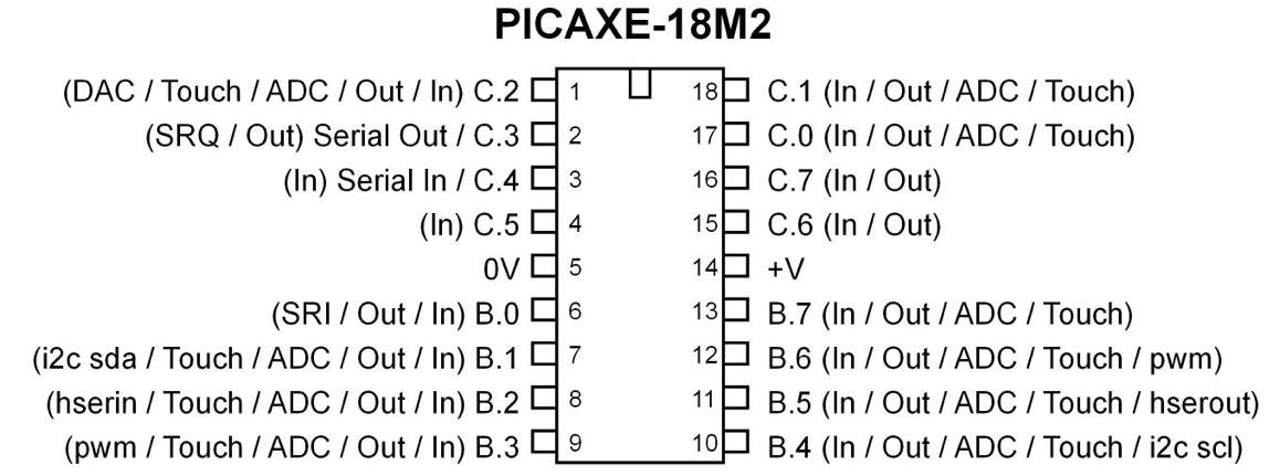
Figure 16 – Pinout of PICAXE 18M2
PICAXE 18M2 has 10 pins for taking analog input. Out of these 10 pins it was decided that pins B.1, B.2, B.3, C.1, C.0, B.7, B.6, B.4 would be used to take input from the FSR sensors (as discussed in the previous section). This pins were chosen as they were capable of taking input and have an ADC.
Pins 2, 3 and 5 were used for the connections of the download circuit as explained above.
Pin 5 was connected to the negative terminal of the battery and pin 14 was connected to the positive terminal.
The connection of the microcontroller with the RN4020 is shown in figure 16.
RN4020
PICAXE 18M2


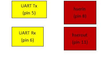
Figure 17 – Connections between PICAXE 18M2 and RN4020
The “hserin” command in PICAXE is used to receive serial data. This is connected to the UART Tx of the BLE module. This was done only for debugging purposes (it would be useful when the programming would be done). So, by making this connection, the transmitter of the BLE module is getting connected to the receiver of the microcontroller.
The “hserout” command in PICAXE is used to transmit serial data. This is connected to the UART Rx of the BLE module. This connection allows the microcontroller to send data to the BLE module. In other words, the receiver of the BLE module is getting connected to the transmitter of the microcontroller.
After studying all the connections of PICAXE with all the other components, the schematic was started.
- Making the schematic (Part 1)
The connections discussed above had to be converted into a schematic diagram. Now, to make the schematic diagram, there are many software available in the market. The two main ones considered were “Eagle CAD” and “Fritzing”.
Eagle is a tool for making printed circuit boards (PCB). Making a PCB in eagle is a two-step process. First the schematic has to be drawn, and then the “switch to board” feature automatically converts the schematic into a PCB (shown in figure 16).
The auto-routing feature automatically connect traces based on the connections defined in the schematic (shown in figure 17).
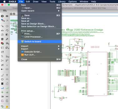
Figure 18 – “Switch to Board” feature in Eagle
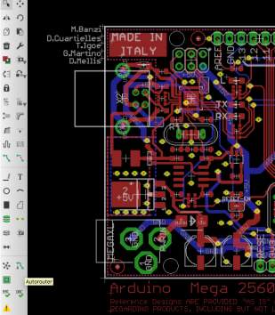
Figure 19 – “Auto routing” feature in Eagle
More features of Eagle will be discussed later in the report.
Fritzing is a very easy to use, open source schematic and PCB making software. It has a unique feature of having a breadboard view of the circuit. This is shown in figure 18 (Instructables).
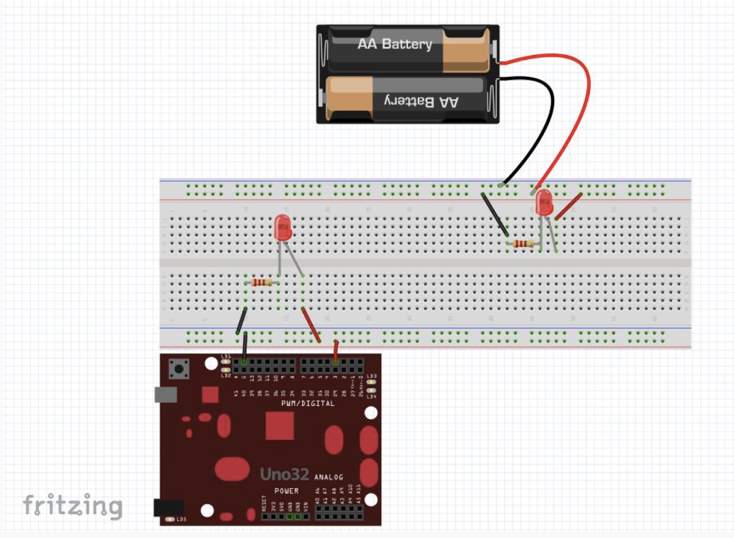
Figure 20 – “Breadboard prototyping” in Fritzing (Instructables)
After considering the pros and cons of both Eagle and Fritzing, they had to be compared to design the PCB. Table 5 shows the comparison between the two.
| Comparison between Eagle and Fritzing | |
| Eagle | Fritzing |
| Used for making schematic and designing PCB. | Used for making schematic and designing PCB. |
| Has no special feature for breadboard prototyping. | Has a special feature of breadboard prototyping. |
| Custom parts can be made | Custom parts can be made |
| Much more extensive part library. | Many parts not available and not very extensive libraries. |
| Less user friendly, therefore a bit tedious to use. | More user friendly, therefore easier to use. |
| Open source | Open source |
Table 5 – Comparison between Eagle and Fritzing
Initially, Fritzing was used to make the PCB being more user friendly. As more and more components were to be added, out of which most were unavailable by default in the Fritzing libraries, it became more difficult to use Fritzing. Components in order to be used had to be made, which would be very time consuming.
Therefore, although Fritzing was easier to use, but due to extensive libraries for components available, Eagle was chosen to make the PCB.
- Making the schematic (Part 2)
As Eagle was chosen to make the PCB, it had to be studied in detail. This report explains the features of Eagle in the order they were used.
The first step was to combine all the connection discussed in the previous sections into a schematic diagram. The circuit was first drawn by hand (attached in appendix 2) in the project notebook and then it was drawn in Eagle. The schematic drawn for the first time is shown in figure 20.
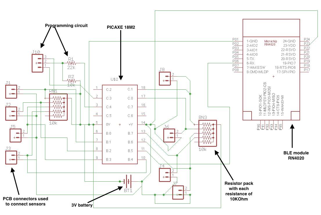
Figure 21 – Schematic diagram – Iteration 1
The first iteration of the schematic diagram is shown in figure 21. This shows the connection of the programming circuit, FSR sensors (via a resistor in the resistor pack), connection to the battery and the BLE module. All the connections for the BLE are not complete in this schematic diagram.
To make this schematic diagram, the following features of Eagle were used:
- Add part – This feature is used to add a component to the schematic. Figure 22 shows how this feature works. The component has to be available in the libraries provided in the package. If the part cannot be found, it has to be either made, or a custom library of the manufacturer of that part has to imported into the Eagle package. For example, the library for PICAXE chips wasn’t available in the Eagle package. The custom library had to be included separately.
- Net tool – After adding the components, they were connected using the “Net” in the toolbar (“Net” and NOT “Line”) (Figure 23). “Net” makes an electrical connection between the two pins, whereas “Line” only draws a line between the two end and doesn’t join them.
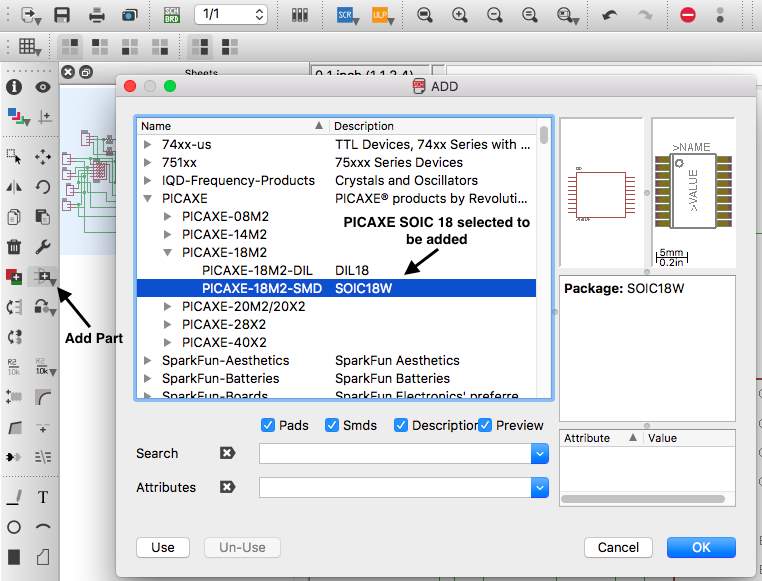
Figure 22 – Add part feature in eagle
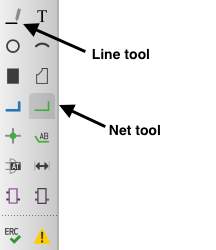
Figure 23 – Line tool and Net tool
- Move tool – This was used to move and place the components correctly (Figure 24).
- Copy tool – This was used to copy a component. For example, as 8 two pin PCB connectors were to be used, it would be very time consuming to add the same component again and again using “Add part”. This is where the Copy tool was found to be useful (Figure 24).
- Delete tool – This was used to delete any component. (Figure 24)
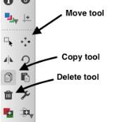
Figure 24 – Move, Copy and Delete tools
- Making the Board
After finishing the first attempt of making the schematic diagram, the “switch to board” (shown in figure 18) was used to convert the schematic into a PCB layout. The first PCB is shown in figure 25.
The wires in figure 25 depict “air wires” (the yellow wires). These wires are not electrical connections, therefore, the air wires have to be converted to electrical connections. There are two ways to convert air wires to electrical connections:
- Using the “Route manually” tool: In this option, each air wire has to be manually routed from the starting point to the end point (figure 26). For more number of connections, it would take a lot of time to route each connection manually. Although this option is feasible for less number of connections.
As shown in figure 26, the two encircled (in white) points had to connected, for which manual routing was used (encircled in black in the toolbar).
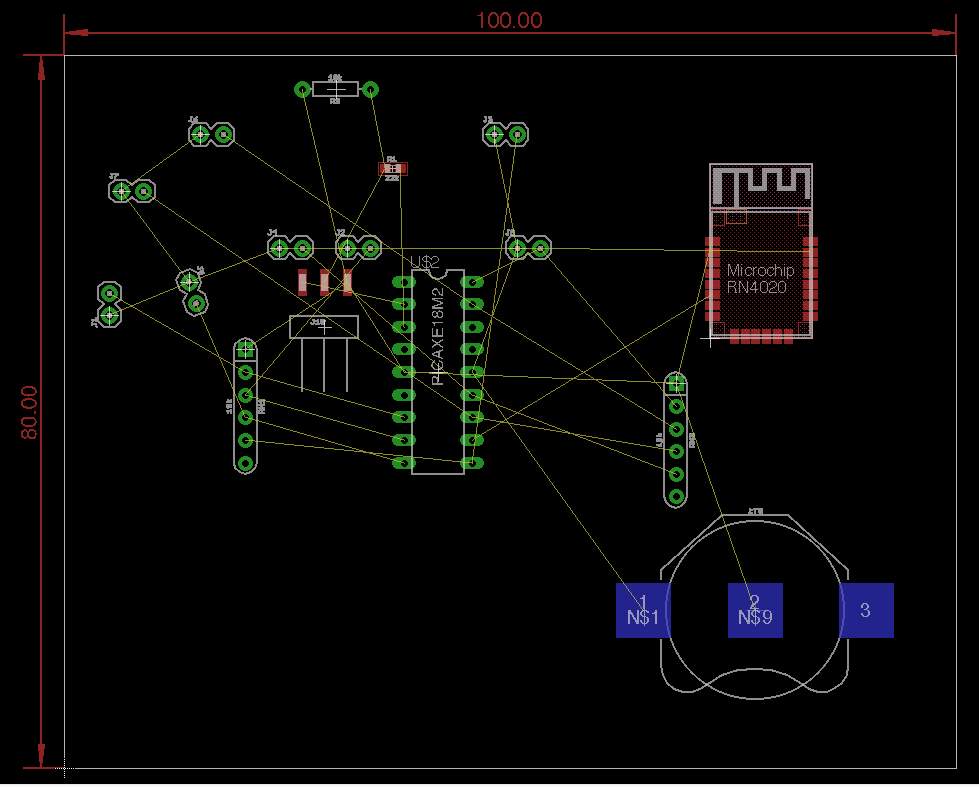
Figure 25 – PCB Iteration 1
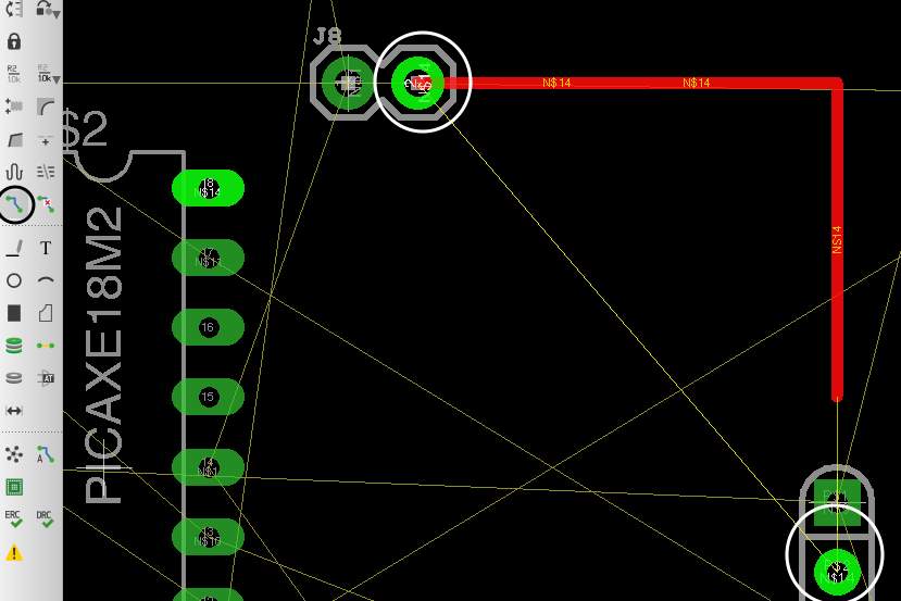
Figure 26 – Route manually tool
- Using “Autorouter” tool: In this option, all air wires are automatically routed. This does not require manual routing of each and every air wire from its starting point to end point.
After routing (manual or Automatic) one thing has to be kept it mind. It is to check whether there are any air wires left after making all the electrical connections. This is more likely to happen when routing manually. To check this, the “Ratsnest” tool is used. This is shown in figure 27.
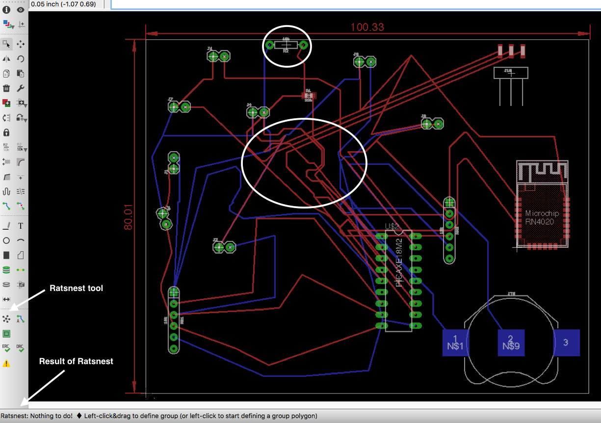
Figure 27 – Using Ratsnest
By checking the results of the “Ratsnest” test, it was clear that no air wires were left in the board. This was evident from the result “Nothing to do!” which can be seen in figure 27. This gave a clear indication that all the electrical connections were made.
- Mirror tool – One more thing to be noted in the board shown in figure 27 is the two different coloured wires – “blue” and “red”. All the connections with the battery are blue in colour. This is because the battery is on the “back side” of the board. In other words, the board will come out to be a double sided board. The battery is put on the back side using the “mirror” tool in eagle (figure 28).
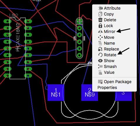
Figure 28 – Mirror and Rotate tool
- Mirror tool – The objects were also rotated using the rotate tool (“Rotate” in figure 28) to be placed properly on the board.
The first board design layout (figure 27) had the following issues:
- A lot of space was there between the components. They could be brought close together to reduce the size of the board. The size of the board in the first iteration came out to be 80.00 mm by 100.00mm (which makes it 8cms by 10 cms).
- Some components were not within the boundaries of the board (encircled in figure 27).
- A lot of wires were overlapping and were very messy (encircled in figure 27). This had to be corrected, as it would short the overlapping connections.
In the second iteration of the board layout, it was tried to fix the above issues, but in the board itself. The schematic was not corrected. The changes were made to the board layout itself.
A good way of checking for the overlaps are, is the “DRC”. In eagle there are two tools for error checking – “ERC” and “DRC”.
The Electrical Rule Check (ERC) is used to check for inconsistencies between the board and the schematic. If changes are made to the board itself, the schematic and the board would no longer be consistent. As a result of this check the automatic Forward and Back Annotation will be turned on or off, depending on whether the files have been found to be consistent or not. Forward annotation is switching from the schematic to the board layout and Back annotation is switching from the board layout to the schematic.
For the subsequent board layout, as the changes were made to the board itself, the “ERC” check was not used much.
The Design Rule Check (DRC) is used to validate the board against certain design rules.
After improving upon some of the design issues discussed previously, the DRC check was done on the board.
The board was validated against the SparkFun design rules (SparkFun). The file was loaded into the eagle package. When the icon for DRC is clicked on the toolbar, it shows the pop up window shown in figure 29.
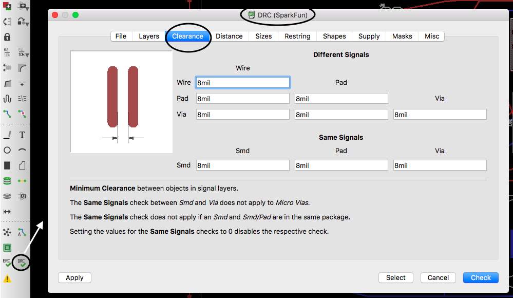
Figure 29 – DRC for error checking
As shown in figure 29, When DRC is clicked, it opens up a pop up window showing the various design parameter the DRC will check the board against. For example, Clearance shown in the figure is the minimum distance which should be maintained between wires, pads, vias, smd etc. In the Sparkfun Design rules files it was set to be 8 mil. This number was not changed for any DRC applied. These parameters can be changed according to the requirements of the project. After all the parameter were set (or predefined as in this case), check option was clicked. This then checked the board against the set parameters and design rules and highlighted the error. This can be seen in figure 30.
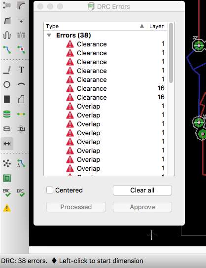
Figure 30 – Errors shown with DRC
As shown in figure 30, there were 38 errors in the board. There were 3 types of error found in the error list:
- Clearance Error – As discussed earlier, this is the minimum distance which should be maintained between any wires, pads, vias, smd components etc. An example of this type of error is shown in figure 31.
- Overlap Error – This is the error caused due to overlap of wires. An example of this type of error is shown in figure 31.
- Restricted Error – This error occurs when a component is out of the boundaries of the board. This error is shown in figure 27.
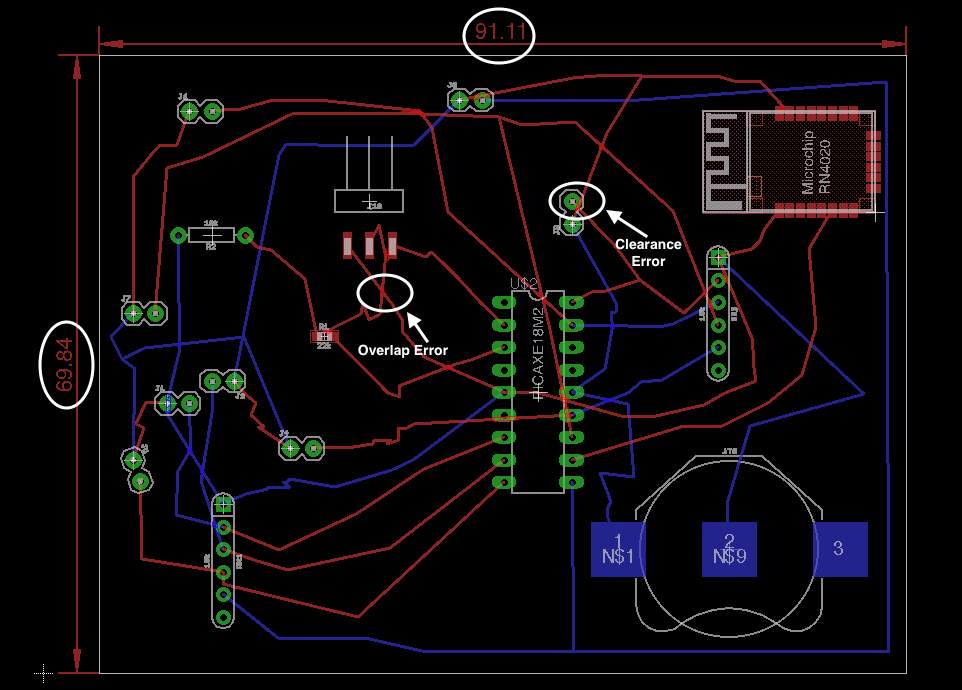
Figure 31 – Clearance and Overlap DRC errors
The second iteration of the board is shown in figure 31. The second iteration was had less messy intersections. Also in this iteration the size of the board decreased significantly. The size now came down to 69.84 mm by 91.11 mm (from being 80.01mm by 100.33mm).
The board still had some design issues:
- The 38 DRC errors had to be removed.
- The board had to be made smaller. The placement of some of the components had to be observed and changed, which could make the board smaller.
These issues were tried to be solved in the next few iterations. The board after some iterations is shown in figure 32.
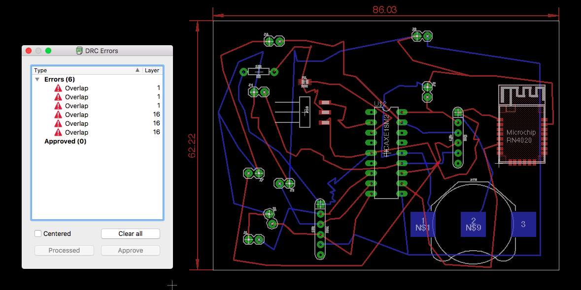
Figure 32 – Board iteration 10
The board shown in figure 32 was formed after over ten iterations. The errors were reduced to only 6 and the board had also become smaller in size (62.22 mm by 86.03 mm)
However, this board also had some issues:
- The PICAXE 18M2 chip used in this board was not surface mount, so it had to be replaced with a surface mount version of it.
- The size of the board was still very big to be used.
In the next iteration, the PICAXE M2 was replaced by its SMD version. The board looked much neater in terms of design. The board after next few iterations is shown in figure 33.
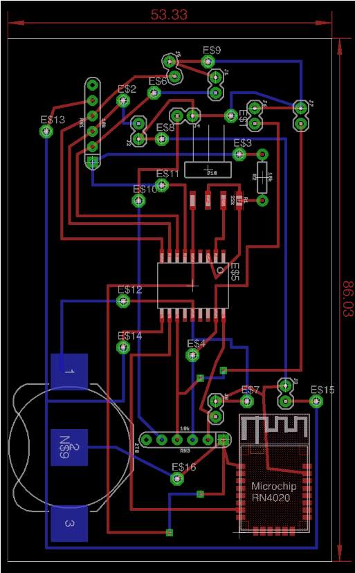
Figure 33 – Board after 20 iterations
The major changes in the board after 20 iterations were:
- The microcontroller was replaced by its surface mount version. This helped in making the board smaller.
- The thickness of the connecting wires was increased from 0.010mm to 0.016mm. This was done to get a better physical board.
- The wires were changed from being curved to being at 90 degrees.
- The length of the board reduced significantly from 62.22mm to 53.33 mm.
- Test pads and Vias were used.
Some of the features of eagle used to make these improvements were:
- Layers Settings: This helped in viewing the 2 layer of the board separately. An example of this setting is shown in figure 34.
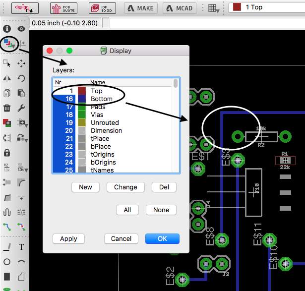
Figure 34 – Layer Settings
As shown in figure 34, When a layer settings tool is selected from the toolbar, a pop up window opens up named “Display”. The “top” layer is unselected. This causes all the red lines (the top layer connections) to disappear. Only the blue lines (the bottom layer connections become visible). This helped in fixing the issues faster.
- Show tool: It is used to see the connections from end to end. An example is shown in figure 35.
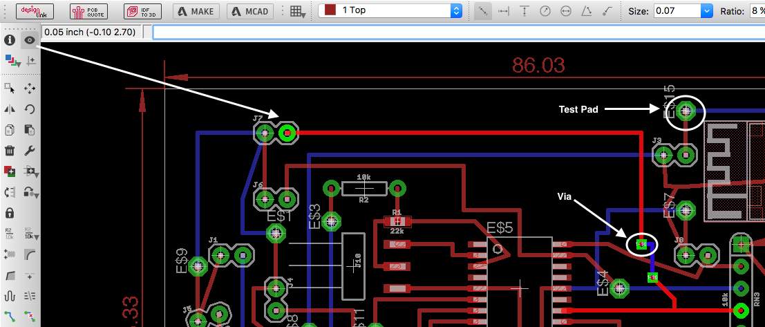
Figure 35 – Show tool
These tool was very helpful in detecting error as it made clear the specific connections. Figure 35 shows the connection of the two-pin PCB connector (to which the FSR would be connected) with an analog input pin of the microcontroller, via a resistor in the resistor pack.This tool helped clear many messy connections.
Vias were used when the intersection of 2 wires was very difficult to fix. An example of a via is shown in figure 35.
Test pads were used to simplify the connection of the top layer of the board with the bottom layer. An example of a test pad is shown in figure 35.
The board shown in Figure 33 very much improved from previous boards in terms of design but there were still issues to be solved with it. The issues with board after 20 iterations were:
- The board was still very big. The size could be reduced by overlapping the battery holder (which is on the bottom layer), with the microcontroller and the BLE module.
- The DRC errors increased to 22.
These issues were handled in the next few iterations of the board. The improved board layout design is shown in figure 36.
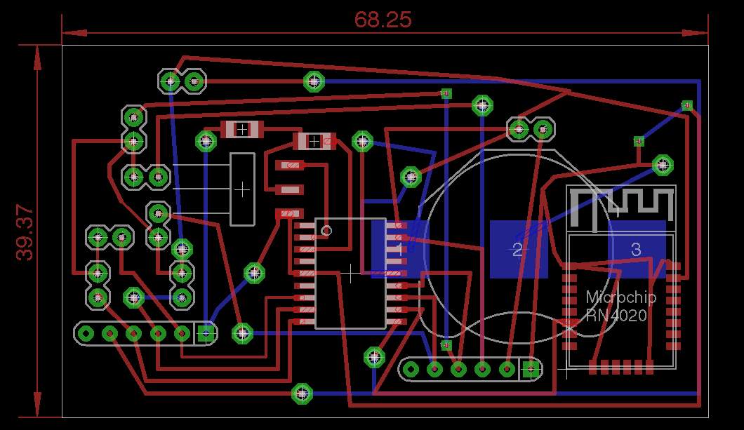
Figure 36 – Board layout after 27 iterations
In the board shown in figure 36, the microcontroller and the BLE module were overlapped with the Battery holder. The board was made even smaller, i.e. 39.37mm by 68.25mm.
Unfortunately, still the board had some issues to be solved. The board shown in figure 36 could be improved upon the following:
- Connection with BLE module were not complete. All connection had to checked and made.
- As most components were surface mount, the resistor packs could be changed to surface mount as well. This could help in reduce the size of the board further.
- The vias used had a very small diameter, which would make it hard to solder when the board was made (physically). Therefore, all vias were replaced with Test pads, as they were solving the same problem.
One major problem was observed with the board shown in figure 33 and figure 36. Majority of the DRC errors in both these boards were caused due to the connections made to the surface mount components. An example of this error is shown in figure 37.
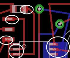
Figure 37 – Error in SMD connections
The connections with SMD parts were errors, because they were not getting connected. These errors had to be removed. Later it was realized that the cause of these errors was, making changes to the board itself (i.e. not having a schematic).
As explained earlier, all the connections were made in the schematic in the initial stages of the board only. Later, the board itself was corrected without making any schematic. As the some of the SMD parts were added later to the board, direct connection (using route tools explained previously) was giving error. This problem was solved by defining an electrical connection first (using the signal tool) and then routing it. This made perfect connections with all SMD components without any errors. A capture of the solved issue is shown in figure 38.
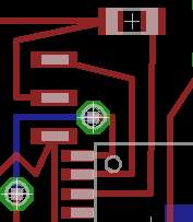
Figure 38 – Error with SMD connection solved
After solving all the issues mentioned above, the final board was produced after about 40 iterations. The final board in shown in figure 39.
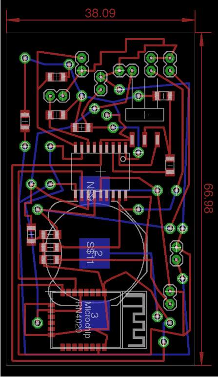
Figure 39 – Final board after about 40 iterations
In the final board, all the discussed previously were solved. The DRC for the final board came out to be zero, and the size went down further to 38.09mm by 66.98mm. The board was not shrunk further, as it would make the soldering very difficult.
A comparison of all the improvements done through all the iterations done to make the board are summarized in table 6 below.
| Iteration 1 | Iteration 2 | Iterations over 10 | Iterations over 20 | Iterations over 27 | Iterations over 40 | |
| Shown in Figure | 27 | 31 | 32 | 33 | 36 | 39 |
| DRC errors | 120 | 38 | 6 | 22 | 23 | 0 |
| Size of board (mmx mm) | 80.01 x 100.33 | 69.84 x 91.11 | 62.22 x 86.03 | 53.33 x 86.03 | 39.37 x 68.25 | 38.09 x 66.98 |
| Improvements | – | DRC errors reduced.
Size reduced. |
DRC errors significantly reduced.
Size reduced further. |
PICAXE replaced with surface mount version.
Size reduced |
Battery overlapped with PICAXE and BLE.
Size reduced significantly. |
SMD connections issue solved.
Connections with BLE completed. Vias replaced with test pads. Resistor packs changed to surface mount resistors. |
Table 6 – Comparison of boards after different iterations
The final board design was selected and printed to proceed with the project. Meanwhile, as the board was getting designed, the Bluetooth app was made and the FSR sensors were tested simultaneously. These will be discussed in the next section of the report.
- Building and testing the Bluetooth App
The Bluetooth had to be made to fulfill the objective of sending the sensor data from the microcontroller to the user’s mobile phone. As it was not possible to test it directly with the PICAXE 18M2 (because the board was in the making), so a similar app was made. The app was initially built to send the phone’s accelerometer data to a computer. It was planned to make changes to the app, once the BLE module is ready to send the data.
The App built was an android app and was aimed to send the phone’s accelerometer data to “Coolterm” running on a computer. Coolterm is a terminal application used to send and receive data from hardware connected over serial ports.
Android studio is used to make android applications. It is an Integrated Development Environment (IDE) owned by Google. This IDE was used to make the Bluetooth application. The next section explains the building of the application.
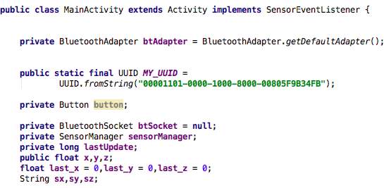
Figure 40 – Bluetooth App variable declaration
As shown in figure 40, the class “MainActivity” extends the Activity class. This class helps an android app to do a single thing. Each Activity performs one focused task and interacts with the user. Next, the class implements the “SensorEventListener” interface. This interface is used to receive the notifications for new sensor data. This can be used for many types of sensors, For example accelerometer, gyroscope etc.
After this an object of the “BluetoothAdapter” class is created (the btAdapter). The BluetoothAdapter is used for fundamental Bluetooth tasks, such as initiating device discovery, querying a list of paired devices, creating a BluetoothServerSocket to listen for connection requests from other devices, start a scan for Bluetooth LE devices etc. The use of Universally Unique Identifier (UUID) will be explained later. Bluetooth Sockets are analogous to TCP sockets. RFCOMM is a very common type of Bluetooth socket, which is supported by the Android APIs. RFCOMM is a connection-oriented, streaming transport over Bluetooth ((also known as the Serial Port Profile (SPP)). The sensor manager is a class that allows access to the android device’s sensors. An object of this class is also created.
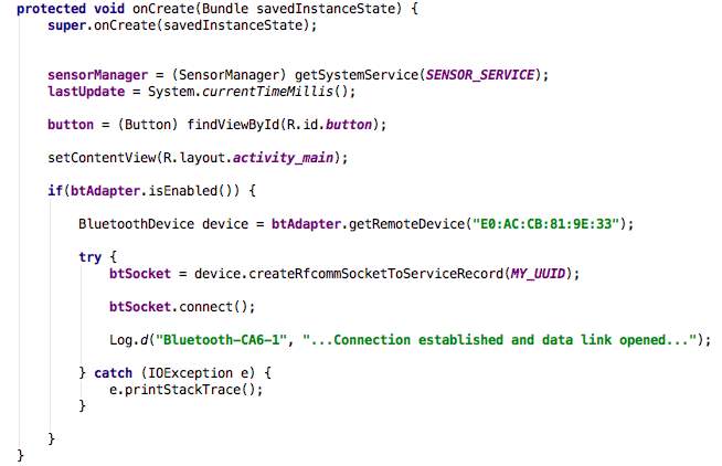
Figure 41 – Bluetooth App onCreate Method
Figure 41 shows the onCreate method of the Bluetooth application. This is the first method called when any android application runs. In this function, the connection is established between the phone’s Bluetooth and the computer’s Bluetooth. The “getRemoteDevice()” is the method used to get a BluetoothDevice object for the device with MAC address provided as an argument. In this case, the MAC address is of the computer system (as the application will be downloaded to the phone). createRfcommSocketToServiceRecord() method is used to create a BluetoothSocket for connecting to a known device (in this case the computer’s bluetooth).The connect() method is used to try a connect to the remote device. After the connection is formed, the data is taken from the accelerometer.
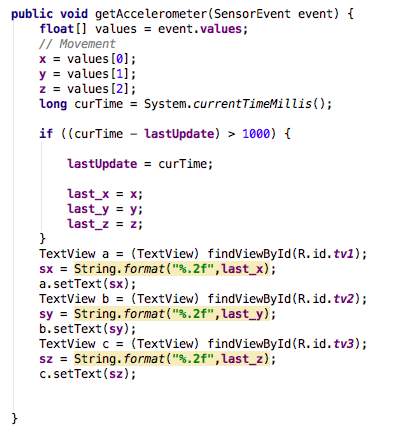
Figure 42 – Taking data from the accelerometer
Figure 42 shows method used to take data from the accelerometer. The if condition is set in such a way, so as to take the data after every second. The variable sx, sy and sz store the value of the coordinates given by the accelerometer.
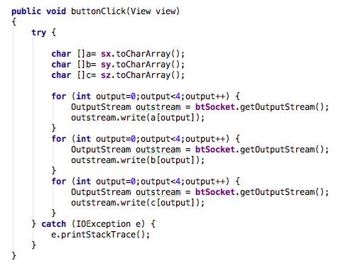
Figure 43 – Method for outputting data to coolterm terminal
The method shown in figure 43 is used to display the data onto the coolterm terminal when the button is pressed. First the values of sx, sy and sz are converted to character arrays. Then they are outputted to the terminal using the OutputStream class and the btsocket.
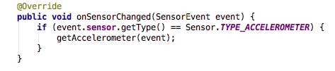
Figure 44 – Selecting the type of sensor
Shown in figure 44, the Accelerometer sensor was selected using the OnSensorChanged() method (see TYPE_ACCELEROMETER). This method triggered the getAccelerometer() method.
The full source code of the Bluetooth Application is Appendix 3.
After the application was ready, it was tested. Figure 45 and 46 shows the Accelerometer data on the phone and on the computer respectively.
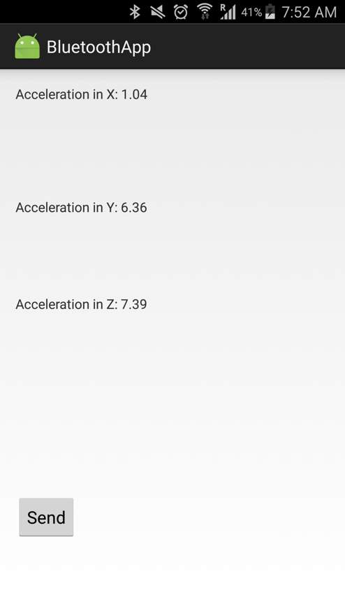
Figure 45 – Accelerometer data on phone
As shown in figure 45, the data was continuously taken from the accelerometer, but it was only sent to the computer when the send button is pressed.
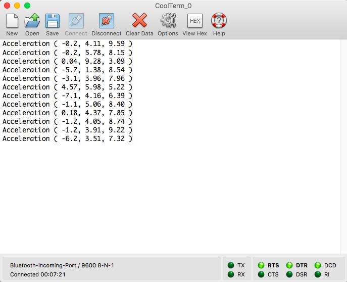
Figure 46 – Accelerometer data on computer
The data sent to the computer is shown in figure 46. The first value under acceleration is the x coordinate, the second is the y coordinate and the third is the z coordinate of the phone. The testing of the FSR sensors is discussed in the next section.
- Testing the FSR sensors
The FSR sensors were tested using an Arduino UNO. The FSR sensor was connected to the analog pin of the Arduino. An LED was connected to an output pin. The LED glowed with the intensity of the pressure applied to the FSR sensor i.e. if more pressure was applied, the LED was glowing brightly and if less pressure was applied, the LED glowed dimly. The flow chart of the program is shown in figure 47. The circuit diagram is shown in figure 48.
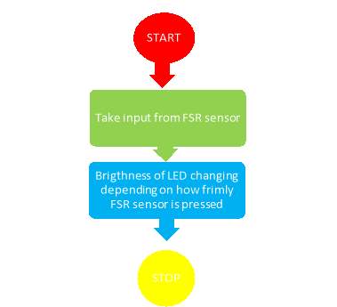
Figure 47 – Flow chart for programming Arduino to test FSR
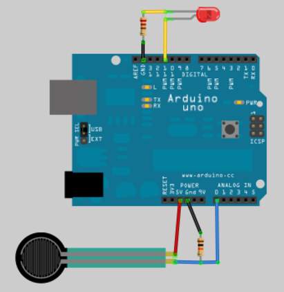
Figure 48 – Connecting the FSR to Arduino for testing
The code was written on the Arduino IDE with the help of the flow chart (figure 47). It is shown in figure 49.
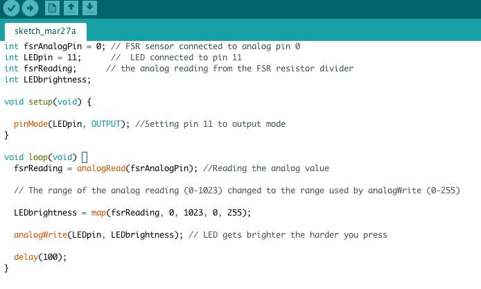
Figure 49 – Arduino FSR to Arduino for testing
As shown in figure 49, the variable named fsrAnalogPin is set to 0, as the FSR sensor was connected to the analog pin number 0. LEDpin is an ouput pin to which the LED is connected (it is pin number 11). fsrReading and LEDbrightness are used to take the FSR analog reading and the brightness value of LED respectively.
The setup() function is the first function which executes when the program is run (its analogous to the main function in C or C++). Within this function, the mode of the pin to which the LED is connected is set to output.
Next is the loop function. First the analog value is read using analogRead() into the variable fsrReading. This reading is mapped from a scale of 0 to 1023, to, 0 to 255 as the latter is the range for analogWrite. The variable LEDbrightness now carries the value which will determine the brightness of the LED. This value is then sent to the LEDpin (to which the LED is attached). The results are shown in figure 50.
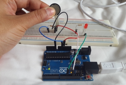
Figure 50 – Testing the FSR sensor
As shown in figure 50, the LED glows when the FSR sensor is pressed. The testing was done to check all the FSR sensors. All FSR sensors were working.
By the time the FSRs were all tested, the PCB was ready to be used. The next section discusses the programming of the microcontroller PICAXE 18M2.
- Programming and Testing the board
The final PCB is shown in figure 51 and 52.
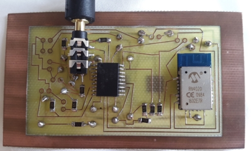
Figure 51 – Final PCB – Top side
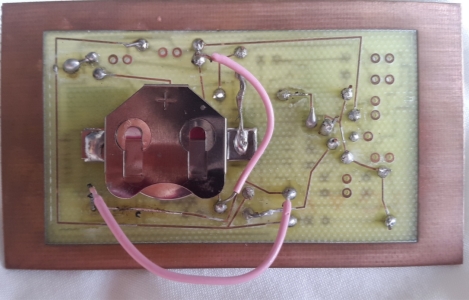
Figure 52 – Final PCB – Bottom side
The holes visible in the figures 51 and 52 are for the 2 pin PCB connectors used to connect the FSR sensors. It was planned to first make all the connections except that of the FSR sensors. This was done to put sensors only if the board is being programmed or is visible on the Blockly Editor used for programming the microcontroller. The flow chart for the program is shown in figure 53.
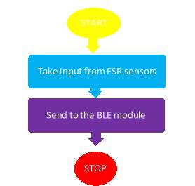
Figure 53 – Flow chart for programming PICAXE 18M2
The “Blockly Editor” for PICAXE was used to write and execute the program. It is a unique editor which lets the programmer to simply connect blocks of the structs used in the program (this can be done in the block mode). It also has an editor (code mode) which lets the programmer simply write a program in word and execute it.
The editor was used for this project to write the program. The main part of the program is shown in figure 54.
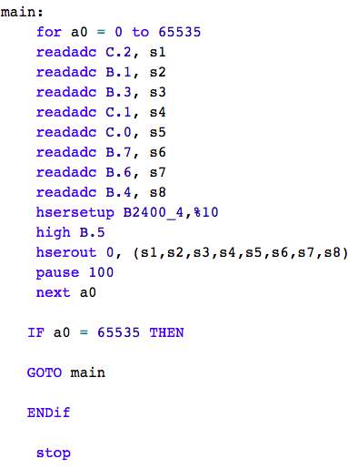
Figure 54 – Programming PICAXE 18M2
As shown in figure 54, All the analog values from the FSR sensors were taken into variables from s1 to s8. This was done using the command readadc. The hsersetup command is used to set the baud rate. Baud rate refers to the number of symbol that can be transmitted per second (not to be confused with bit rate). All PICAXE chips support a baud rate of upto 4800. On the other hand, the RN4020 module is woken up by a baud rate of 2400 or above. Therefore, it was decided to set a baud rate equal to 2400. The pin B.5 is the one which acts as the transmitter of the PICAXE 18M2. This pin is set to high and hserout is used to send all the values from s1 to s8 are sent out. Pause keyword is used to cause a delay of 100 ms (so that the data gets through in this time). All this is performed within a loop which is running with the value of the variable a0. The loop is 65533 times (as this is the maximum value a variable can be assigned). The “if” loop does the trick of making the program run infinite times. When the value of a0 reaches its maximum, it is sent back to the label “main”. This program takes in data from the FSR sensors and sends it to the BLE module. The full code is attached in appendix 4.
Unfortunately, when it was tried to load the program onto the microcontroller, the software wasn’t able to find the PICAXE chip. The error shown by blockly is shown in figure 55.
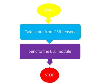
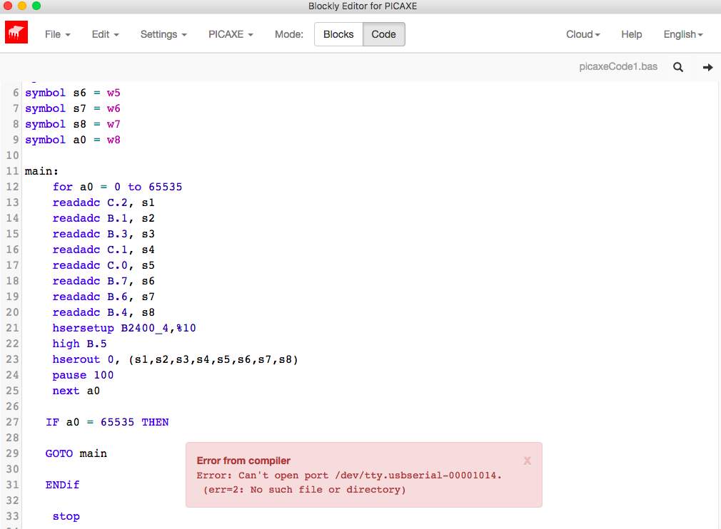
Figure 55 – Error while programming PICAXE 18M2
Due to this error the microcontroller could not be programmed. The connection of the cable was checked; a continuity check was done for all the connections on the board after the board completed. All this was done, but the board did not work. More about this issue would be discussed in the next section.
This section may also be presented as two separate sections of Results and Discussion. The convenience of whichever style to be adopted may vary from project to project (your supervisor will provide guidance on this).
The Results section is where data are presented as tables or figures and your should consider the following when writing this section:
(a) Decide which data are best presented in a tabular format and which are best presented in a graphic formatavoid presenting the same data in both formats;
(b) Summarize each data presentation by addressing the relevant trends or patterns that pertain to the project hypothesis or objective(s). These summaries should be written clearly and concisely, avoiding personal pronouns and excessive descriptive phraseology. Write quantitatively mention of terms more or less, doesn’t tell much. How much more or less? Use the data in your writing, such as, 65 percent of the ball bearings seized compared to only 45 percent of the roller bearings.
(c) Present the strongest, most compelling data first and the weakest, least compelling data last. When the sections are presented separately, do not make interpretations nor draw conclusions about the data in the Results section; this is left to the Discussion and Conclusion sections.
The Discussion section is where interpretations are made and conclusions drawn about whether the results support or fail to support your stated hypothesis. The following should be considered when writing this section:
(a) State the strongest, most convincing data of your argument in support or rejection of the hypothesis first, followed by progressively weaker evidence. Refer to your data presentations to provide evidence of your position;
(b) Include comments on how design inadequacies and experimental errors might have affected your results and what could be done to reduce them.
- If there has been similar research done by others, state how your work compares;
- State the relevance of the experiment to the field of research and where new directions of research might lead from this experiment
Conclusions are often the most difficult part of the Final Year Design Project reportmany students feel that they have nothing left to say after having written the report. However, you need to remember that the conclusion is often what a reader remembers best, hence, your conclusion should be the best part of your report.
The good Conclusion should review the entire project against your problem definition, aims and objectives, and evaluate project success and results. It may also include a section for suggestions for further work, or if these are many, then a Further Work chapter may follow the Conclusion. The following suggestions will ensure a good set of conclusions:
- Show why your project was important show that your project was meaningful and useful;
- Conclusions should synthesize, not just summarize contents in the main body of the report should not simply be repeated. You need to outline how the points you have made and the support and examples you used were not random, but fit together.
- Redirect your readers Give the reader something to think about, perhaps a way to use your design/results in the “real” world. If your introduction went from general to specific, make your conclusion go from specific to general, i.e., think globally.
- Often the sum of a good final year design project is worth more than its partsBy demonstrating how your ideas in the project have worked together, you can create a new perspective to similar applications.
Use IEEE referencing.
Salient components of the project planning should be described, and critically evaluated with suggestions for how the project planning could have been improved upon in case significant deviation from original plans had to be accommodated in the project. For example, indicate how your project monitoring or prescribed milestones raised any issues and if you needed to re-plan your project at any point(s).
Present the salient extracts from your project diary over the two semesters.
Drawings (sketches, mechanical, electronic drawings etc.) are necessary, as part of the design process, hence; layout drawings, detail drawings and assembly drawings, where possible, should constitute part of your design project report.
- Bluetooth Application code
package com.itb.bluetooth;
import android.app.Activity;
import android.bluetooth.BluetoothAdapter;
import android.bluetooth.BluetoothDevice;
import android.bluetooth.BluetoothSocket;
import android.hardware.Sensor;
import android.hardware.SensorEvent;
import android.hardware.SensorEventListener;
import android.hardware.SensorManager;
import android.os.Bundle;
import android.util.Log;
import android.view.View;
import android.widget.Button;
import android.widget.TextView;
import java.io.IOException;
import java.io.OutputStream;
import java.util.UUID;
public class MainActivity extends Activity implements SensorEventListener {
private BluetoothAdapter btAdapter = BluetoothAdapter.getDefaultAdapter();
public static final UUID MY_UUID =
UUID.fromString(“00001101-0000-1000-8000-00805F9B34FB”);
private Button button;
private BluetoothSocket btSocket = null;
private SensorManager sensorManager;
private long lastUpdate;
public float x,y,z;
float last_x = 0,last_y = 0,last_z = 0;
String sx,sy,sz;
@Override
protected void onCreate(Bundle savedInstanceState) {
super.onCreate(savedInstanceState);
sensorManager = (SensorManager) getSystemService(SENSOR_SERVICE);
lastUpdate = System.currentTimeMillis();
button = (Button) findViewById(R.id.button);
setContentView(R.layout.activity_main);
if(btAdapter.isEnabled()) {
BluetoothDevice device = btAdapter.getRemoteDevice(“E0:AC:CB:81:9E:33”);
try {
btSocket = device.createRfcommSocketToServiceRecord(MY_UUID);
btSocket.connect();
Log.d(“Bluetooth-CA6-1”, “…Connection established and data link opened…”);
} catch (IOException e) {
e.printStackTrace();
}
}
}
@Override
public void onSensorChanged(SensorEvent event) {
if (event.sensor.getType() == Sensor.TYPE_ACCELEROMETER) {
getAccelerometer(event);
}
}
public void getAccelerometer(SensorEvent event) {
float[] values = event.values;
// Movement
x = values[0];
y = values[1];
z = values[2];
long curTime = System.currentTimeMillis();
if ((curTime – lastUpdate) > 1000) {
lastUpdate = curTime;
last_x = x;
last_y = y;
last_z = z;
}
TextView a = (TextView) findViewById(R.id.tv1);
sx = String.format(“%.2f”,last_x);
a.setText(“Acceleration in X: ” + sx);
TextView b = (TextView) findViewById(R.id.tv2);
sy = String.format(“%.2f”,last_y);
b.setText(“Acceleration in Y: “+sy);
TextView c = (TextView) findViewById(R.id.tv3);
sz = String.format(“%.2f”,last_z);
c.setText(“Acceleration in Z: “+sz);
}
public void buttonClick(View view)
{
try {
char []a= sx.toCharArray();
char []b= sy.toCharArray();
char []c= sz.toCharArray();
char []d= “Acceleration ( “.toCharArray();
OutputStream outstream = btSocket.getOutputStream();
for (int output=0;output<15;output++) {
outstream.write(d[output]);
}
for (int output=0;output<4;output++) {
outstream.write(a[output]);
}
outstream.write(‘,’);
outstream.write(‘ ‘);
for (int output=0;output<4;output++) {
outstream.write(b[output]);
}
outstream.write(‘,’);
outstream.write(‘ ‘);
for (int output=0;output<4;output++) {
outstream.write(c[output]);
}
outstream.write(‘ ‘);
outstream.write(‘)’);
outstream.write(‘
‘);
} catch (IOException e) {
e.printStackTrace();
}
}
@Override
public void onAccuracyChanged(Sensor sensor, int accuracy) {
}
@Override
protected void onResume() {
super.onResume();
sensorManager.registerListener(this,
sensorManager.getDefaultSensor(Sensor.TYPE_ACCELEROMETER),
SensorManager.SENSOR_DELAY_UI);
}
@Override
protected void onPause() {
super.onPause();
sensorManager.unregisterListener(this);
}
}
- Programming the PICAXE 18M2
symbol s1 = w0
symbol s2 = w1
symbol s3 = w2
symbol s4 = w3
symbol s5 = w4
symbol s6 = w5
symbol s7 = w6
symbol s8 = w7
symbol a0 = w8
main:
for a0 = 0 to 65535
readadc C.2, s1
readadc B.1, s2
readadc B.3, s3
readadc C.1, s4
readadc C.0, s5
readadc B.7, s6
readadc B.6, s7
readadc B.4, s8
hsersetup B2400_4,%10
high B.5
hserout 0, (s1,s2,s3,s4,s5,s6,s7,s8)
pause 100
next a0
IF a0 = 65535 THEN
GOTO main
ENDif
stop
Technical documents such as standards, component specifications, formulae sheets and formulae derivations may be included in this appendix.
Cite This Work
To export a reference to this article please select a referencing stye below:
Related Services
View all


Related Content
All TagsContent relating to: "Medical Technology"
Medical Technology is used to enhance the medical care and treatment that patients are given in healthcare settings. Medical Technology can be used to identify, diagnose and treat medical conditions and illnesses.
Related Articles
DMCA / Removal Request
If you are the original writer of this dissertation and no longer wish to have your work published on the UKDiss.com website then please: