Monitoring Noise or Interference Found in Power Supply
Info: 14247 words (57 pages) Dissertation
Published: 16th Dec 2019
Tagged: Engineering
POWER LINE MONITOR, PLC – BASED TO MONITOR SPIKES
ABSTRACT
This report talks about the ideology of monitoring noise or interference found in any power supply. Several methods are shown to aid understanding of the design and development of this system.
It explains the use of a programmable logic unit (PLC) for a representing voltage and current graphically to ensure correct monitoring of voltage and current spikes.
Some components were used in the project of which includes the programmable logic controller (PLC), HMI (human interface machine), one DC motor, current sensor, a J-K Flip-Flop and voltage comparator. The motor was connected to a DC power supply which supplied the voltage with distortion and the current sensor measured the current from the supply.
An analogue to digital converter (FX2N-2AD) was used to convert the generated analogue signals of the voltage and current to equivalent digital values.
Furthermore, the GX IEC Developer software was used to create the program logic to read and manipulate the converted digital values and convert them to understandable values.
The PLC consists of a HMI screen which is a display screen that is touch sensitive and was used to display the graphical representation of the current and voltage signals.
J-K Flip-Flop and voltage comparator were later introduced as additional hardware components of the system. The hardware components involved in this project will be discussed in more details later in this report.
Lastly, this report discusses about the errors encountered and ways used in resolving them.
GLOSSARY
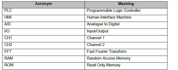
Table 1- Acronyms
- Introduction
Monitoring Power supply is very essential to ensure a clean power input by many industries and domestic applications.
A low quality of power results a very bad quality of service, therefore consistency and steadiness of a powerline are significant factors for industries especially in order to avoid possibility of substantial financial losses. Examples of Some sectors that suffered financial losses due to low power quality are:
Semi-conductors production with financial loss per incident of €3800000
Financial trade with financial loss per incident of €6000000 per hour
Computer centre with financial loss per incident of €750000
Telecommunication with financial loss per incident of €30000 per minute
Steel industry with financial loss per incident of €350000
Glass industry with financial loss per incident of €250000
Offshore platforms with financial loss of €250000-€750000 per day
Dredging/land reclamation with financial loss per incident of €50000-€2500000 per day
Therefore, a poor power quality with a supply often comprises of various examples of spikes, amplitude change and uneven harmonics.
This project is focused on monitoring the spikes that occur through a powerline, with the use of a PLC to build a powerline monitoring system to display spikes that occur through a supply with generated poor power quality.
Power supply consists of a fully sinusoidal voltage waveform with continuous amplitude although this isn’t a scenario of due to non-zero impedance within the supply.
Power quality is often defined as the electrical network’s or the grid’s ability to supply a clean and stable power supply. In other words, power quality ideally creates a perfect power supply that is always available, has a pure noise-free sinusoidal wave shape, and is always within voltage and frequency tolerances.
- Project AIM and Objectives
This section shows the aim of the project as well as the objectives taken to achieve various stages of the project. The aim is result that is expected to be achieved at the end of the project with the help of the objectives.
- AIM
The aim of this project is to analyse and monitor power supply noise more effectively with Proper selection and wise operation of programmable logic controller (PLC). This can be made possible by developing a hardware stem to do the monitoring. This idea or method can be used by industries to save costs in carrying out such task.
The Hardware system developed is connected to the PLC to be programmed for getting voltage and current readings from a supply. The current and voltage parameters are taken from the PLC registers, displayed on the HMI screen and observation of spikes can be carried out.
- Objectives
The above aim will be accomplished by fulfilling the following project objectives sated below.
- Proving the ability to monitor and detect power qualities, focusing primarily on spikes formed in a power line from a supply.
- Designing, developing, and building the hardware unit to detect and display unwanted signals with the use of DC motor to supply the voltage and a current sensor to detect the current Passing through the circuit.
- Using an analogue-to-digital(A/D) converter to translate the readings coming from the analogue signal in the circuit into digital values.
- Implementing a ladder logic through the GX IEC Developer software onto the PLC to read the digital data obtained from the circuit by the A/D convertor and storing the data registers.
- Sampling and displaying the digital values on a Human Machine Interface (HMI) screen to monitor the spikes that occur through the system.
- Transferring the data onto Microsoft Office Excel® performing Fast Fourier Transform (FFT) to analyse the data obtained and prove an appropriate sampling rate
- Implementing a voltage comparator and J-K Flip-Flop to develop the hardware unit to use a LED as an indication whenever a spike occurs.
- Project Feasibility Study
Before starting the project, it was needed to confirm that the entire project could be completed successfully and weather its costs would be more than its benefit. In the feasibility study, a checklist is being followed to make sure various resources concerned with the project will be available to complete the project.
Furthermore, it is concerned with the organisation of the project in order to have a complete project at the estimated project time with the aid of a Gant chart.
The PLC –based power line monitoring system for spikes provides a cost effective and time efficient path for industrial applications, service providers and their customers. With all the said investigations
and proposed time plans, it was deduced that this project is feasible.
- Costs of Project
The table below gives a detailed breakdown of the cost of the project, the components without prices were provided by the university and this table can prove the cost of the project is less expensive for industries as earlier stated in this report.
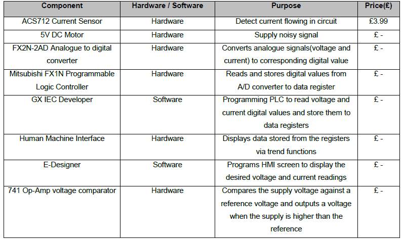
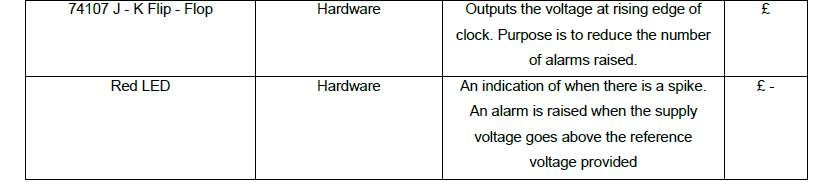
Table 3 – Costs of resources
- Marketability
The performance of a device under distorted supply voltage is not guaranteed due to low power quality which can cause the device to operate abnormally and also permanent damage. Therefore, manufactures introduce devices to the market guaranteed it will perform correctly with a supply voltage that is sinusoidal.
So, Poor quality can lead to excessive financial losses that affects customers and service providers. It can be very hard to deduce the exact figures of financial losses sometimes.
Many Devices sensitive to supply distortion and instability are owned by customers. Therefore consumer surveys are carried out to investigate and compare problems like voltage dips and harmonics within the power sector. It is proven that this problems are increasing yearly.
Many accounts of costs made by poor power quality in industries and service sectors can be seen as estimated in the survey for EU’s 25 countries in 2008.
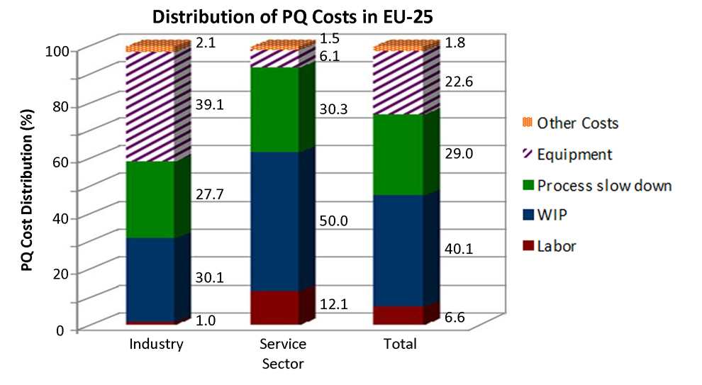
Figure 1 – Power Quality costs [2]
Observing the power instabilities present in supplies and areas affected, it is understood that there is a necessity for development of systems that are able to monitor noise and instability within a main supply. By monitoring this irregularities, quality of power being supplied would be known by consumers and then any form of distortion may be corrected when reported.
It is concluded that manufacturing a system that is capable of Using PLC to monitor spikes has great marketability. The level of this project is gigantic because it has many applications and can also be upgraded to monitor other malformation present in a system. With increase in technology, PLC’s are frequently used and it can be incorporated to simplify and enhance performance.
PLC’s are getting more advanced than generators and it is present in almost all production line and machine functions. PLC has many advantages and one major advantage is the ability to be reprogrammed and change an operation during its stage of assembling and manipulating important information. The multitasking ability of a PLC is incredible that it handles input and output devices in way what will be suitable for the particular application.
- Report Guidance
Introduction – This section talks about the overall commenced project work and the report written for documentation. The aims and expected objectives to achieve at the end of the project, along with the reasons for undertaking this project is included in this part. Other related and equally vital topics such as the project’s feasibility and marketability have also been included.
Literature Review – This section is based on research undergone over the project time. It documents vital information and practices needed to be understand the project. It contains the necessary topics such as power quality and the functionality of PLCs along with examples of programming.
Design And Development – This section explains the work completed through the time of the project. This chapter is further split into 4 subsections, the initial segment shows and examines the general system. The second division altogether portrays the outline of the hardware. The following component is committed to clarifying also, understanding the product strategies utilized as a part of request to empower this system to be completely utilitarian and discloses the methods used to get data. In conclusion, the fourth subsection gives learning on an extra thought fused inside the hardware and demonstrates its usefulness.
Results Analysis – This section observes the result outcomes accumulated from the system. what’s more, clarifies the strategies utilized. It additionally talks about any constraints found through this procedure.
Conclusion – The conclusion incorporates a brief outline of the whole report and project work and takes note any remarks or suggestions. Notwithstanding, subjective and quantitative discussion of the project, ideas for potential further improvement for this project is also included.
1.4 Summary
In this area, general report structure and project work were talked about. The aims and objectives anticipated that would have been accomplished at the end of the project have been expressed, along with the explanations behind undertaking this project. Costs of project material have been recorded
Furthermore, the attractiveness or marketability of the project have additionally been examined.
The accompanying chapter talks about the literature review completed over the project term.
2 Literature Review
Keeping in mind the end goal to completely comprehend the job needing to be done, related background studies were performed before continuing to start the project. This literature review looks into the related fields to all the diverse components that make up the project. This part aims to clarify power quality, what’s more the related issues that could possibly be exceptionally harming. This then prompts to examinations particularly towards spikes alone to shows how different inductions of spikes (voltage, current and power) influence power quality. It additionally talks about the techniques which could prompt to determine, secure and enhance these abnormalities. Notwithstanding the hypothetical research undergone, this area additionally talks about the foundation of viable resources taken for this project, specifically Programmable Logic Controllers. It will focus on its design and the different applications. finally, it will likewise demonstrate its significance towards this project.
2.1 Power Quality
Electrical supplies, being something that are being underestimated and anticipated that would be made superbly accessible quickly yet is not considered to have many foundation forms passed on before it is given to power points. A wide range of parts, for example, clinics and relentless creation lines utilize gadgets that are extremely dependent on solid and stable voltages arriving to their buildings. These necessities construct inquiries and enthusiasm for the nature of the electrical cable moving toward all the different segments [3]. Power quality is depicted as the level of closeness a power supply has to the properties of an “ideal” power supply. An ideal power supply would comprise of a completely “clean” sinusoidal voltage signal. Lamentably, this thought today is only hypothetical and power supplies with flawless properties are non-existent. There is in any case, techniques to order power supplies to be considered as “great” or ‘awful’. A supply with “great” power quality would be demonstrated with any connected loads performing palatable and won’t create expansive expenses. Be that as it may, one with a poor power quality would bring about the heaps coming up short, having less lifetime and would additionally bring high money related expenses
2.1.1 Implications of Poor Power Quality
Having a poor power quality has numerous outcomes whether it be a minor or major unsteadiness. These hazards could possibly bring about disappointment or breaking down of gear, overheating gadgets, for example, inside transformers or engines and extremely delicate hardware that require steady stable energy to finish a procedure (PC PCs, generation lines, healing facilities ETC). Different results of poor power quality incorporate power supplies falling flat out of the blue, which can be recognized by circuits blowing and their breakers stumbling very every now and again. Power hazards may likewise prompt to obstruction being available inside the system, bringing about electronic interchanges to be traded off and be made exceptionally temperamental. In expansion to these worries, because of the additional electrical anxiety, site establishments should be larger than usual which would raise establishment expenses and running expenses significantly. Alongside this, it would deliver a higher carbon footprint. It is likewise conceivable that these destinations would have their whole associations declined and evacuated since it would taint the supply network by an extensive sum. All these talked about suggestions prompt to a certain thing, a diminishment in proficient lifetime [1].
Client surveys completed worldwide on electric supplies demonstrate that voltage plunges are one of the power quality issues that causes significant bothers and have a basic money related outcomes. Money related misfortunes because of voltage plunges are chiefly focused to customers as they are the people that are influenced the most.
These effects rely on upon various things be that as it may, primarily the kind of gadgets and occasions being disturbed, the span of the gathering of customers being influenced, and the classes the clients are put in. Moreover, it is too watched that distinctive customers experience diverse misfortunes as these money related effects rely on upon the sort of occurrence happened and the seriousness of that occasion. Looking into distinctive reviews, designs demonstrate that intrusions that are short are the more noteworthy givers to power quality related expenses and economic losses [1].
As indicated by the European power quality survey which was done over a two year time span (a long time 2003 – 2004), practical misfortunes of more than 150 billion Euros are brought up in the EU- 25 nations [Targosz and Manson, 2007]. This study was brought forward through 62 different benefit areas, notwithstanding extraordinary enterprises. From the aftereffects of this survey, it was perceived that 90% of the whole money related misfortunes are because of the enterprises [2].
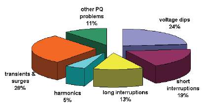
Figure 2 – Percentage of economic losses across EU-25 countries [2] Figure 2 – Percentage of economic losses across EU-25 countries [2]
Figure 2 delineates the rates of financial misfortunes that are experienced in the EU-25 nations, and the different power quality factors these exist in. as shown,56% from the aggregate money related misfortunes are because of voltage dips and interruptions, 28% of the expenses are expected to drifters and surges and the other 16% of budgetary misfortunes are available because of sounds, glimmer and EMC related issues [2].
2.1.2 Causes of poor power qualities
Taking note of the quantity of disasters poor power quality can bring about, brings up an issue of why. The primary benefactors to this issue are receptive power which superfluously stacks up the supply framework, consonant contamination which makes establishments to run less productively by including an extraordinary measure of additional weight on the electrical systems. Lopsidedness of load likewise add to this, in which they may bring about creating extra worry to connecting loads that are associated on to a similar network.
2.1.3 Protection and improvement techniques
Looking at the problems examined already, it is concluded that there is an appeal for poor power qualities to be enhanced or ensured against. Any size of ‘terrible power quality being introduce in a framework can affect not just the framework (perpetual harm or lessening lifetime), in any case, could likewise influence the people in charge of the framework (monetarily or even physically).
Enhancing Power Quality
Nature of gear inside a modern framework is specifically connected to the way the hardware is grounded and reinforced. Erroneously grounded gear influences the most extreme execution accomplished by the framework. There are two varieties of a grounded association, one being a grounded conductor (unbiased) and the other being security ground, and the distinctions are extremely essential. The security ground is the association that grounds the gear and it ensures the device alongside the electrical framework from sudden covering voltages, for example, unintentional high voltage contact or when lightening happens. Alongside this, it additionally keeps the development of static charges. Keeping in mind the end goal to forestall perilous conditions inside a framework, the wellbeing ground must comprise of an impedance way between the hardware to the holding point and the administration begin point establishing anode. This impedance way ought to be sufficiently low for blame streams sufficiently high to clear the circuit hinders in the framework. The grounded conductor (unbiased) is a conductor clung to one purpose of the establishing framework and conveys current. By doing this, the voltage potential inside the hardware is restricted with reference to grounded parts. Immense economic losses can be limited with right and appropriate establishing and holding [4].
Another procedure to enhancing power quality is to decrease power unsettling influences. Normal cases of force unsettling influences incorporate voltage changes and commotion, and they exist in a wide range of structures, for example, harmonics, frequency and spikes. From these dangers, harmonic distortion has become a noteworthy issue on account of the expanded utilization of electronics. In harmonic distortion, nonlinear current (contrasted with the voltage waveform) is drawn by the electronic equipment and causes high impartial current, voltage mutilation, breaker stumbling, and overheated transformers.
The Information Technology Industry Council (ITIC) overhauled a CBEMA bend which characterizes the working voltage measures in which the gear ought to work dependably in 2000. Figure 3 demonstrates the bend and the marked envelopes that demonstrate the working states. Devices must be ready to adapt to unsettling influences that lie in the “no interruption” region, as found in the chart. At the point when a voltage aggravation enters the “no-damage” area, the device may not work not surprisingly but rather it could recoup as the voltage returns back to normal. The hardware worked may turn out to be for all time harmed if these unsettling influences come to the “prohibited” area. Security against entering the “prohibited” and “no damage” ranges is required for equipment that is extremely costly and crucial, and that moreover rely on upon solid supplies.
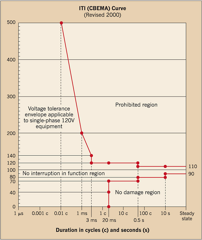
Figure 3 – Voltage operating envelopes [4]
Protection from power disturbances
Throughout the years various gadgets have been made and built up that intend to secure equipment against any power aggravations that happen, by improving the power came to the framework. This area records and depicts a few cases of these insurance gadgets.
Filters
These secure electrical equipment against low voltage-high frequency noises. They work by permitting the vital frequencies, as expressed by standard (typically 50 or 60 Hz), to pass and obstructing any higher frequency noise, for example, electromagnetic impedance (EMI) and radio frequency interference (RFI). filters particularly intended to control the stream of harmonic current inside a framework are called harmonic filters.
These filters keep any consonant substance from nonlinear loads being passed back to the source.
 Figure 4 – Active Tracking Filters
Constant Voltage Transformer (CVT)
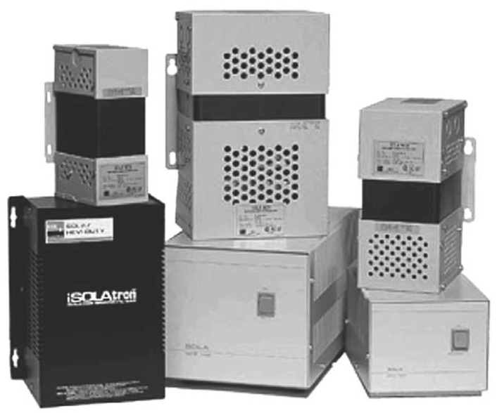
Figure 5 – CVT
It is also called a ferroresonant transformer, it is a sort of voltage controller. CVT, being a completely static controller, maintains a nearly consistent voltage yield when there are incredible deviations in input voltage. Constant voltage transformers accompany numerous focal points, for example, an exceptionally exact output voltage, more isolation of noise and overload security by current constraining.
Uninterruptible Power Supply (UPS)

Figure 6 – UPS
An uninterruptible power supply is a system which gives “reinforcement” control if there should be an occurrence of a total interference all through the whole power network (power outage). UPS is generally utilized where loss of power making systems go disconnected, is inadmissible (for instance clinics and server rooms in schools). The usefulness of UPS is to convey a steady supply of force in a whole length of complete power failures. Notwithstanding power outages, they give security against noise, power surges or sags, contingent to the kind of technology incorporated.
2.1.4 Voltage Spikes
Voltage spikes are types of power disturbance that happen through networks driving from electrical supplies. Voltage spikes can be characterized as the sudden, flashing increment in supply voltage through an electrical circuit and these spikes occur for a brief timeframe [5]. Another, more specialized, meaning of voltage spikes is that they are short lived, quick electrical drifters in voltage [6]. The name “spikes” for these short-terrm increments in supply voltages are offered because of the shape framed when they are seen with test equipment, for example, oscilloscopes. The sudden ascent in voltage seems like a spike on the display
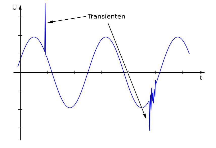
Figure 7 – Voltage Spike
The effect of electrical spikes can extend from recoverable to calamitous. Typically electrical spikes cause the remaining current gadgets (RCD) to trip. These pieces are electrical security switches which keep high voltages and streams from passing through an electrical circuit. Contingent upon the capacity, a stumbled RCD can totally close the power to a whole building or parts of that building. Luckily, stumbled RCD’s can just be reset to the working position to reestablish control(power). Be that as it may, with no RCD assurance, voltage spikes can harm every single electrical equipment associated, for example, PCs, sound systems and TVs.
Alongside this, if an electrical spike enters a phone circuit it is additionally equipped for harming web switches(routers). if there are damaged devices the best option is to replace them, adding to the money related misfortune to customers [5].
2.1.5 Current Spikes
force anomalies can be in form of current spikes that emerge inside electrical circuits from supplies. Current spikes are normally brought about by lightening, demonstrating a sudden increment and fall in the supply. This can possibly result in serious harm by breaking through insulation that is intended for a typical supply. This will more often than not leave a thin portion of copper, which in time can prompt to a short circuit.
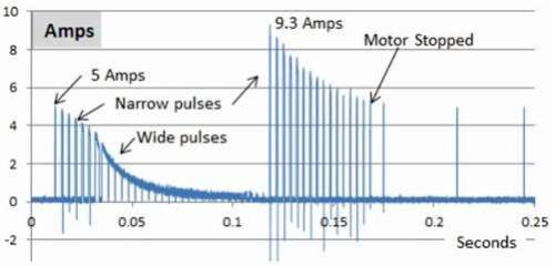
Figure 8 – Current spikes
It is in the voltage’s properties to create a relating increment in current when there is voltage spike. In spite the fact this is the standard, it is at times watched that the inverse happens. The voltage spike is incited to increment as required with a specific end goal to keep up a consistent current stream. One case of this is of the current from an inductor when it is releasing. In delicate electric circuitry, additional measures of current can stream depending if a voltage spike increments past the breakdown voltage of a device. Inordinate electric streams can seriously debilitate on the other hand even forever damage the equipment when in semiconductor junctions. equipment can be ensured through numerous overvoltage securing devices, for example, torrential slide diode, transient varistor or voltage suppression diode to redirect or shunt the transient current.
2.1.6 Power Spikes
Alongside voltage and current spikes, another phenomena called control spikes are likewise present inside electrical cable or power lines. Control spikes have the capability of comprising of to a great degree high voltages amid short beats of vitality. Despite the fact that they generally keep going for a couple of milliseconds, they can achieve peaks of more than 6000 volts.
Because of the brief span in which the power spike occur, complete equipment failure does not generally happen, but rather there most unquestionably is the capacity to bring about awesome harm to extremely fragile devices prompting to enormously disastrous incidents.
A much more damaging situation is the likelihood that while devices may not flop quickly, performance of the device could gradually reduce and the equipment could flop later once presented to spikes or exposed to spikes. This happens on the fact that semiconductor equipment or devices can be halfway damaged and “debilitated”. Luckily, power supply technology at present upheld is fit for sifting through sufficient measures of these high frequencies and high voltages exhibit over the electrical cable or power line. Regardless of this, there are still quite often recognizable blunders in sound and adulterated information inside advanced devices. furthermore, because of these flaws as still there, further filtering and voltage clipping in electrical cables can be performed for more sensitive equipment alternately important applications with a specific end goal to propel the change towards noteworthy decrease of power spikes.
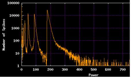
Figure 9 – Power Spikes
2.1.7 Spikes Protection Techniques
From the three varieties of spikes talked about beforehand, it is seen that there is a requirement for assurance from these aggravations bringing on genuine debilitation on essential devices possessed by numerous producers, ventures or even clients. This segment talks about the distinctive techniques for security; voltage constraining devices and current restricting devices.
Voltage Limiting Devices
From figure 10 it can be perceived how a procedure to secure an input port of a VLSI (Very Large Scale integration) segment can be accomplished device ordinarily has a high impedance at typical voltages and does not have any effect on system execution or performance. It is when there is a voltage that outperforms a predetermined edge, that the terminal impedance diminishes and quickly occupies the current far from the vital component.
Figure 10 – Voltage limiting
Varistors
These are generally produced using metal oxide powder and are another kind of voltage constraining device. Like diodes, they additionally have limit voltages yet can be planned with voltages going from 0.5 volts to voltages in the 10’s. Their preference over diodes is that they can disseminate more vitality. Be that as it may, they are inconsistent for flag applications that are of high speed because of the higher parasitic capacitance they contain
Thyristors
Likewise like diodes, thyristors are semiconductor devices and are equipped for scattering a much more prominent measure of vitality contrasted with diodes. A much higher assortment of edge voltages can be uses on thyristors. Be that as it may, much not at all like varistors and diodes, thyristors are “crowbar gadgets”. This implies they short when the voltage that enters is more prominent than the limit voltage, in this manner decreasing the voltage over the part to very nearly zero
Gas Discharge Devices
In early years, two pointed metallic sorts finish off would be utilized as lightning security for phone equipment. This would enact when the voltage distinction over the metal strips would surpass the edge voltage, bringing on the halfway air to break and shape a circular segment. Current uses of this are fundamentally the same as yet utilize devices that are encased in gas filled plastic or glass barrels. Gasses are utilized as opposed to air as it breaks down with more sureness. Contrasted with the past illustrations, gas release gadgets are equipped for scattering more vitality with no damage. Likewise, their property of comprising of low capacitance lessens the probability of mutilation of high recurrence signals.
Particularly like thyristors they are crowbar gadgets, however are fit for holding edge voltages of 10 volts to 100 volts. For the fact that when these devices do come up short, they bomb as an open circuit yet don’t meddle with the applications ordinary operation. A case of devices utilized for these sorts of uses are neon globules, as they carry on fundamentally the same as gas release tubes.
They are additionally a sparing technique for conveying insurance against spikes with a limit of around 70 volts.
Current Limiting Devices
Current restricting devices are parts that are actuated by change in current as opposed to sudden adjustments of voltage. Cases of these devices incorporate circuit breakers, wires and thermal protection devices. They normally have a low impedance however once higher streams are passed they get to be distinctly open and comprise of a higher impedance. Associating these devices in arrangement with the electrical cables and the secured system empowers them to obstruct any power from achieving the equipment without scattering any power as warmth. This guarantees a hypothetical boundless measure of force these devices can deal with. The inconvenience of current restricting devices is that they regularly don’t have a low reaction time to protect important equipment from any quick transient, for example, lightning.
2.2 Programmable Logic Controllers
This area examines an accessible framework which gives the capacity to plan and implant a strategy for control. It upgrades a short sighted view on programming to make different projects what’s more, offer unlimited applications.
Programmable Logic Controllers (PLC) are particular varieties of a microchip based controller which store guidelines and perform works on battery-supported, non-unstable programmable memory. They can perform rationale, timing, numbering and math capacities to control different applications and procedures. Because of the straightforwardness of programming requiring, programmable rationale controllers are planned in such an approach to be utilitarian by designers with restricted programing learning.
PLC’s have been preprogramed in such a way, to the point that the program dialect is observed to be simple to take after and make. It comprises of a progression of coherent strides that are worked of various exchanging operations. For instance, these directions could incorporate a type of “if statements” as; if “A” or “B” happens, then complete operation ‘C’. In this illustration, “A” and “B” speaking to input parameters and “C” speaking to the output. The information devices could be switches or indeed, even sensors and output devices inside the system might be LEDs or motors. An arrangement of directions are “composed” into the PLC making a program of controls put away into the memory.
The operation of the executed program can then be checked to control selected output in light of the contributions as per the usefulness of the program.
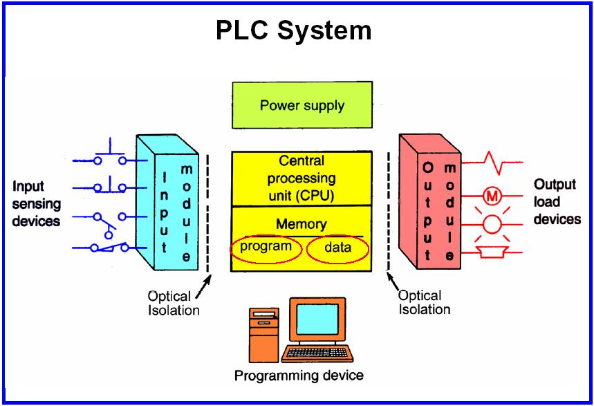
Figure 11 – PLC architecture
PLC operation cycles comprises of four essential stages; Input Scan, Program scan, Output Scan, and Housekeeping. It is called an operation cycle due to the conduct of the operation stream; they are persistent rehashing circles of stages. Figure 12 outlines the phases that the PLC works in. Underneath records the motivation behind every progression towards the usefulness of a PLC.
- Input Scan – this step is responsible for detecting all the connected input devices and their states.
- Program Scan – this stage exists to read and execute the logic programmed by the user.
- Output Scan – at this point in the cycle, the output devices are either activated or deactivated depending on how the program is created.
- Housekeeping – this stage provides the essential post programming actions, such as correct programming terminal communications and internal diagnostics.
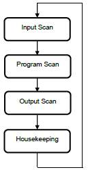
Figure 12 – PLC Operating Cycle
2.2.1 PLC Hardware
The input and output section and the different devices that can be incorporated as sources of input and output were likewise recorded. A lasting capacity limit is accessible because of the memory for utilization of the working system for the information utilized by the CPU. permanent data for the working system is put away in the PLC’s read only memory (ROM), while its random access memory (RAM) is utilized to store status data particularly for the sources of inputs and outputs, and furthermore counters, clocks and other inward devices.
Programming devices can be support devices or a PC, and they are used to transfer projects and data onto the CPU [12].
The central processing unit, otherwise called a CPU, contains an inward stage that can control the PLC usefulness. The customer’s projects comprises of control guidelines, and their execution is controlled by the CPU. The client’s projects are spared into memory that is most certainly not unstable. The CPU is likewise intended to speak with different devices such us other programming devices, inputs/output, systems and furthermore different PLCs. Notwithstanding these, the CPU is likewise mindful to perform “housekeeping” activities, for example, interior diagnostics
2.2.2 PLC Internal Architecture
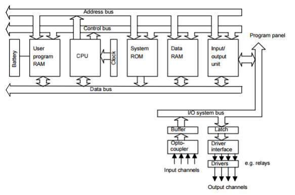
Figure 13 – PLC Architecture
Figure 13 shows a good layout and design of a PLC. Its illustrates that the PLC is made up of numerous sections. The CPU, I/O connections and memory. Operations done within the PLC are handled or controlled by the central processing uni that’s isn being supplied with a clock frequency that defines the PLC operating speed in addition to providing time and synchronisation for the system. For information that flow within the plc, buses are the internal routes. Basically buses are simply the number of conductors where electrical signals flow. They can be wires within a cable or tracks on a PCB. Information is sent through data buses between the different sub sections by the central processing unit. For access to information stored, the address buses are used to send location and the internal control signals are manged by the control buses,
The CPU
Its interior structure fluctuates as indicated by which microprocessor is utilized, yet they ordinarily contain
- Memory, termed registers- these are located inside the microprocessor and are used as data storage for information related to execution of the program,
- The Arithmetic Logic Unit (ALU) – this is the area responsible for performing mathematical calculations which includes addition, subtraction, division and multiplication of data. It is also responsible for carrying out logic operations of “NOT”, “OR”, “AND” and “”XOR”(EXCLUSIVE OR).
- Control Unit – this is the area responsible for performing the management of operation timing.
The buses
As mentioned earlier, these are communication areas inside the PLC. These buses convey information in binary form, which means that a group of bits are passed across single routes. These groups of bits are called ‘word’. For example the binary form 10101010 is called 8-bit word. Therefore words travel along their own assigned parallel wire for it to perform simultaneous communication.
A PLC is comprised or=f 4 different buses:
- Data bus – data gotten from the CPU are being transferred by the data bus.
- Address bus – the address bus makes sure each word can be found since each memory address is given specific value
- Control bus – all the control signals used by the CPU operation is transferred by the control bus
- System bus – it allows connection between input and output ports with I/O unit which enables them to communicate.
Memory
This section comprises of numerous memory elements, the different types with their roles are:
- Read Only Memory (ROM) -It gives the CPU and operating system fixed information storage that is permanent.
- Random Access Memory (RAM) – its divided into two sub sections
- Access for data – its used to store details on input/output devices status and also counter timer values alongside other data from other internal devices
- Access for user programs.
- Erasable programmable read only memory (EPROM) – This is a memory version of ROM that is capable of programming and the program could stay permanent. EPROMs are not really considered as standards on PLCs but are available as a connectable add-on.
Input and Output unit
The PLC is meant to respond based on changes or activities that happen outside the system. This is possible because of the input and output unit. The I/O block allows connection between the I/O channels and the device. The input connection could include sensors or switches, while the output device expected to be functions could be motors solenoids.
2.2.3 PLC Programming
This area introduces the PLC programming language, talking about the fundamental building blocks. Also illustrating example of programs that could be implemented.
PLCs uses the programming style called ladder logic. This technique is implemented in form of blocks generating logical illustration of working system. It is a user friendly programming for engineers with less knowledge and experience of programming.
Below is a few basic symbols that are frequently used when programming with ladder logic.
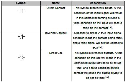
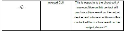
Table 4 – Description of basic symbols
There are also functional blocks alongside with this symbols which are alternative techniques used in ladder logic programming. This is used sometimes when dealing with complex ladder logic programs and they are have the ability to perform mathematical, counter and timer operations.
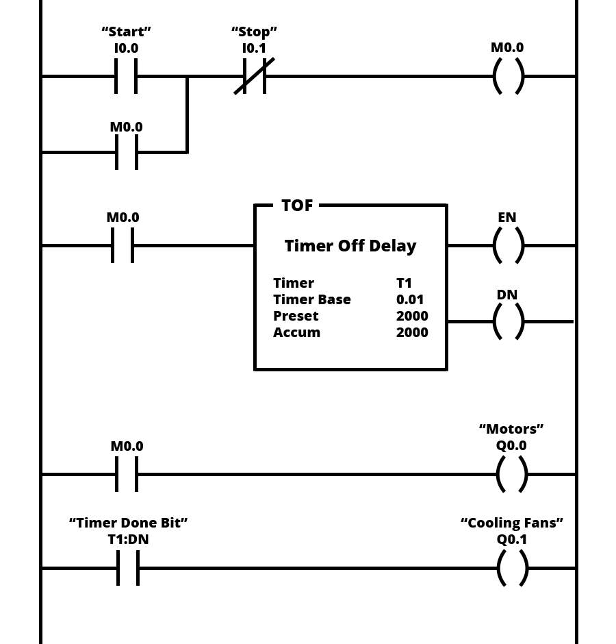
Figure 14 – Typical Ladder Logic diagram example
Here are some examples of fundamental ladder logic implementations.
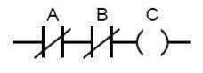
- NAND gate
 the implementation needs one input to be false for the output to be true
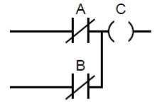
- AND gate
 the inputs are meant to be true for the output “c” to be true.
- OR gate
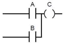 in this case “A” or “”B”, can be set as true for activation of the output “C”.
- XOR gate
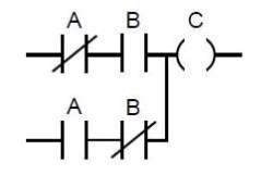 it makes sure the output will never be set as true and if the input is set as true while the other is set as false, it then successfully implements the XOR gate.
- NOR gate
 both inputs may be set as false for there to be true in the output.
- NOT gate
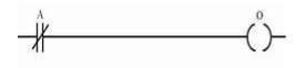 The output contains the opposite condition the input is set to.
It is noticed or observed that ladder logic programming looks similar to the connections within an electromechanical relay considering the control circuit.
For example, a case of two switches that are used to control staircase lights, it is expected that if any of this switched are turned on then the bulb should switch on and with one extra toggle of any switch, the bulb should turn off. Figure 15 below shows how this control is implemented as wired diagrams using two switches and bulb while figure 16 shows the same staircase operation implemented using gates. Using “NOT”,”AND” and “OR” gates processed from a FPGA or integrated chip.
Finally, figure 17 shows the implementation of the two versions of staircase example designed via ladder logic.
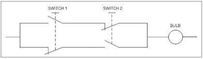
Figure 15 – Wiring Diagram of staircase example
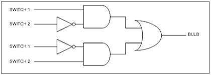
Figure 16 – Staircase example with logical gates
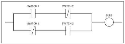
Figure 17 – Staircase example with ladder logic
2.3 Summary
This section talked about the essential background of the project that was researched for the project time. It shows the vitality of a good power quality and talks about the different techniques that can improve power quality. PLC architecture and basic programming knowledge needed to understand ladder logic implementation talked about in the next chapter. The nect section discusses design and development of the actual project done.
3 Design and Development
This area is focused on the development and design methods which was used to complete project. This chapter is divided into four sections, the first is an overview of the system. The second part talks about the description of the design used for the hardware. The third section clarifies and giving insights on the software techniques used to aid the functionality of the system.
Lastly, the fourth section gives additional idea incorporated within the hardware and proves how it functions.
3.1.1 Project Structure
The idea of this project is to plan a monitoring system that can identify distortion – “spikes” for this situation – this a case due to poor power quality. This framework or system utilizes a PLC to program the system to effectively monitor the signals. This project likewise expects to accumulate and store tests of information with the goal of dissecting these undesirable signals moving through the powerline.
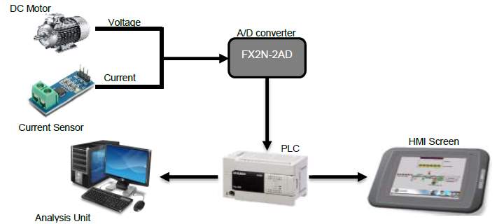
Figure 18 – Project set up
The project structure comprises of a DC engine that provisions the voltage with commotion added to the line. The present sensor (ACS712) is connected with this line to gauge the current got from this power supply. The current and voltage signals are converted to relating advanced values by the analogue to digital converter (FX2N-AD) and are sent to the PLC which is customized to peruse these put away computerized values, scale them to representable figures and store these qualities in data registers. This data is then shown onto the human interface machine (HMI) as charts, obviously demonstrating the spikes that happen. This HMI is given as a part of the PLC system. The three data sorts (current, voltage and power) downloaded from the PLC were then sent to Microsoft Office Excel® to be dissected.
3.2 Hardware Development
This project is applicable towards unwanted signals in AC source but Due to safety concerns and not to violate risk assessment policy, it wasn’t possible to access main power.
Nevertheless, the knowledge of the subject area remains the same and isn’t changed. A system or framework was built to produce like unregulated power to replicate distortion (mainly spikes) within the supply.
Mirroring this mains supply abnormality was proficient through giving a supply of 9 volts by means of a DC motor which super-forced twisting and voltage spikes onto the supply. This distorted voltage supply then was grabbed by the A/D converter and after that the PLC. In expansion to this, the impedances framed in the voltage likewise brought about there to be mutilation and spikes within the current signal. This effectively permitted a worthy representation of undesirable or unwanted signals to be made for further advancement and examination.
3.2.1 Allegro ACS712 Current Sensor
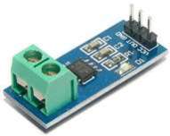
Figure 19 – Allegro™ ACS712
Current Sensor
The Allegro® ACS712 gives prudent and exact answers for AC or DC current detecting in mechanical, business, and correspondences frameworks. The device bundle considers simple usage by the client. Average applications incorporate engine control, stack location and administration, exchanged mode control supplies, and overcurrent fault protection.
The device comprises of an exact, low-balance, straight Hall sensor circuit with a copper conduction way situated close to the surface of the bite the dust. Connected current coursing through this copper conduction way creates an attractive field which is detected by the incorporated Hall IC and changed over into a corresponding voltage. The main aim of using this current sensor on this project was to measure varying current present in the powerline.
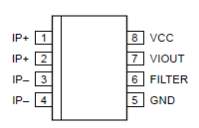
Figure 20 – Pin out Diagram
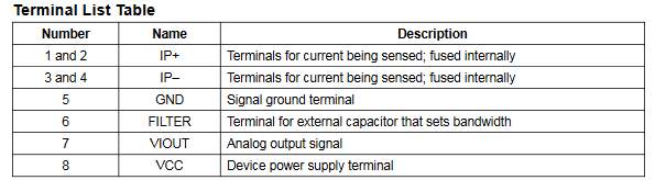
Table 5 – Pin Description
The project required the current sensor to measure the current. Although, as seen from the table above, the output of the current sensor was in volts. Therefore, when using a voltage current relationship, the voltages could be converted to a corresponding current value.
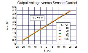
Figure 21 – Output Voltage vs Sensed Current
The equation between current being sensed and the output voltage is y =x/5+ 2.5
Where y = output voltage
X = sensed current
Which was rearranged to give x = 5y – 12.5
Substituting output voltage and sensed current into the equation gives I = 5v – 12.5.
3.2.2 FX2N-2AD A/D Converter
The FX2N-2AD converter was used to convert voltage and current signals into discrete digital values. It allows two separate channels to be connected simultaneously. Channel 1 and 2 were connected with voltage and current outputs respectively. The converted parameters were transferred to the PLC for further manipulation.
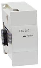
Figure 22 – FX2N-2AD
Module
The converted data transferred to the programmable logic controller is commenced from using FROM and TO instruction available in the ladder logic library.
From the datasheet, it shows that the two input channels 1 and 2 have the ability of receiving inputs of ranges, 0 to 10v, 0 to 5v or even 4mA to 20mA. This is only possible when both inputs are of the same nature.
3.2.3 Programmable Logic Controller
Converted signals from the FX2N-2AD module were transferred to the PLC.
Read and write instructions were applied on the PLC in order to take the values from theFX2N-2AD and store them in data registers using TO and FROM instructions.
Below are some features of the programmable logic controller:
- It consists of 15 inputs labelled X0 to X14
- Integrated LEDs
- 15 output relays labelled Y0 to Y14
- It needs 24 volts of DC power supply to start up
- It uses ladder logic programming but capable of using other programming styles
3.2.4 Human Machine Interface

Figure 23 – Human Machine Interface
The PLC makes uses of a human machine interface (HMI) which is a display screen. The HMI is a graphical interface that’s allows visual representation of a program, also offering an interactive experience for operators.
For this project, the HMI used was Mitsubishi E1071 which is a touch screen which is user friendly.
This panel consists of a real-time clock, integrated buzzers and also passwords facilities for security. Furthermore, the HMI is able to incorporate a printer report functionality and also capable of being designed to show several trend functions such as line graphs, bar graphs and others. Another software used with the HMI is called the e-designer that is used to design implemented ladder logics and downloaded to the HMI after being checked for errors. The E-designer would be explained better later on in the project.
3.3 Software Development
This segment examines the software’s utilized over the time of the project which were actualized inside the equipment components. This area will be part into a further two subsections, in which the principal division will clarify the product application utilized relating specifically to programming the programmable logic controller. The second subsection will talk about the relating human machine interface programming bundle executed to plan the design of the graphical UI. Alongside this, the second subsection will additionally represent how the information was recovered from the plc utilizing the E-Designer programming.
3.3.1 GX IEC Developer
The GX IEC Developer is a dominating programming stage conveying usability through a Microsoft Windows environment for quick, natural programmability onto the Mitsubishi PLCs. This involves speedy and exceptionally effective PLC application executions. This software drops programming overheads by a significant sum with its simple access to much of the time utilized squares, permitting complex projects to be made without the need to a great degree scan for pieces. This product stage gives an extensive variety of choices for programming styles to be actualized, permitting tailor-made programs to be made that best suit the application. The platform supports a range of five language sorts that can be implemented; ladder logic, STL, SFC, IL and FBD. The ladder logic style was chosen and actualized to meet the aim of PLC programming. It was organized to peruse and compose information from the simple to advanced converter and store this data in data registers inside the PLC.
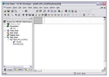
Figure 24 – GX IEC Developer Main Body
Features of the GX IEC developer is listed below
- “Libraries Minimum downtimes”
- “Function blocks (FB, FC)”
- “Online program modification”
- “Powerful offline simulation”
- “Programming languages FBD, AWL, KOP, AS and STC”
- “State-of-the-art PC software technology acc. to IEC 1131.3”
- “Superior program documentation for easy understanding”
- “Flexible program development”
- “One programming software for modular and compact PLCs (Q/A and FX Series)”
- “Suited to large and complex projects”
- “Total overview of PLC project and resources”
- “Powerful “Top-down” development environment”
As stated earlier in the report, ladder logic library contains functional blocks as well as contacts.
Separate blocks used to program the plc is listed below:
FROM_M: this block was used to read the digital value of selected channels after A/D conversion.
Key:
N1 – n1 is the Connection for module address
N2 – n2 is the first address of the module
N3 – n3 represents number of data words
D – Represents destination address to save the data
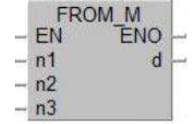
Figure 26 – Functional Block: FROM
TO_M: this block was used for selecting required input channels of the FX2N-2AD module and also initiates the analogue to digital conversion.
Key:
N1 – n1 is the Connection for module address
N2 – n2 is the first address of the module
N3 – n3 represents number of data words
S – Memory address of the data source
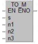
Figure 25 – Functional Block: TO
MOV_M: this block moves data from a specific source to a selected destination address.
Key:
S – Source address
D – Destination address
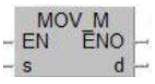
Figure 27 – Functional Block: MOVE
MUL_M: this functional block multiplies two values whether it’s two address content, two integer digits or one of each.
Key:
_IN – inputs the variable: memory address or integer value
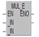
Figure 28 – Functional Block: MULTIPLY
DIV_M: this functional block provides functionality of dividing two values, even if they are two memory address contents, two integers or one of each.
Key:
_IN1 – It inputs the first variable to be computed
_IN2 – it inputs the second variable to be computed
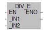
Figure 29 – Functional Block: DIVIDE
SUB_M: this block provides functionality of subtracting two values, be it memory address contents, two integers or one of each.
Key:
_IN1 – it inputs the first variable to be completed
_IN2 – It inputs the second variable to be completed
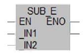
Figure 30 – Functional Block: SUBTRACT
3.3.2 E – Designer
This E – Designer programming is made accessible by Mitsubishi. It is a programming stage that gives a simple and productive technique for outlining and creating graphical UIs on a progression of human machine interfaces. It incorporates an efficient squares utility which demonstrates a full design of the whole venture. The product likewise has quick access to the different images and protests that can be put into the workspace effortlessly. This GUI engineer guarantees that the project final product is easy to see, before downloading onto the equipment.
The software platform promotes the following features:
- Very intuitive help menus
- Importing and exporting project data
- ‘Drag and drop’ feature for GUI creation
- Windows based environment
- Library of graphics such as symbols, objects, trend functions.
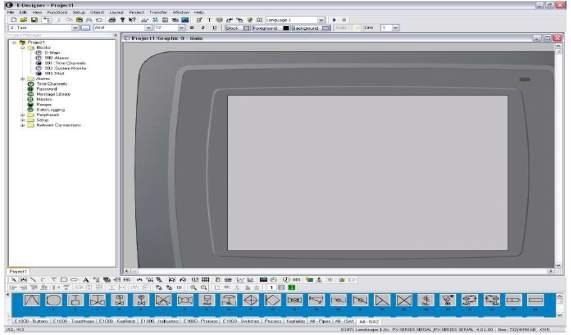
Figure 31 – E-Designer Main
The Trend function
Trends are used as funtions to save and show data from a controller in graph forms.
The amount if trends that can be applied within a project is limitless but only depending on the capacity of the operator panel memory. E-designer software used for this project took advantage of function trends, historical trends and real-time trends.
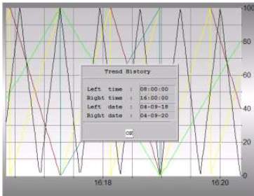
Figure 32 – Trend Function
Figure 32 ahowa rend example which can be included by selecting “trend” button on the tool bar. Trends showing real-time feed can be “paused” to show historical information. By selecting the required trend function followed by “enter” key this is made possbile. After this, a dialog box pops up labelled “trend history”. It enables operators to specify date and time intervals to show corresponding data.
Trend functions were downloaded to a HMI which was a touch screen and the trend functions were upgraded to give better interactive interface. The following table shows interactive functions avialable for HMI touch screens.
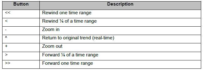
Table 6 – Touchscreen HMI function
Initialising Trend functions
As stated earlier, addition of trend functions are achived by selecting the “trend” icon from object tool bar. Once inserted, a pop up dialog simila to the one in figure 34 appears.
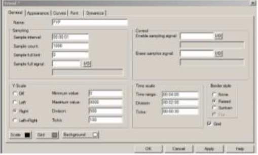
Figure 33 – Generals tab setup
The table below illustrates a description of different parameter trend that are important towards the outcome of HMI for thios project.
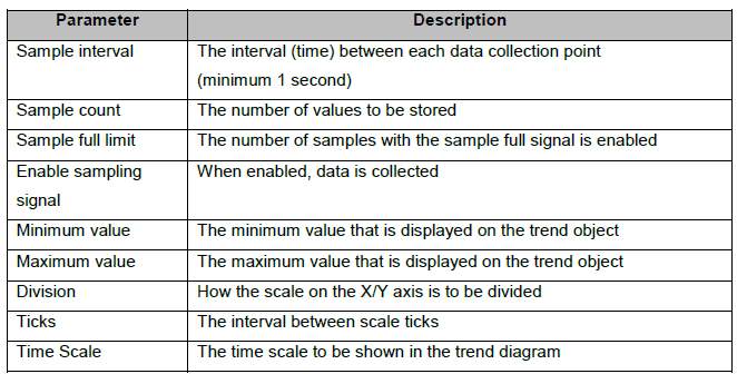
Table 7 – Generals tab parameters
Another viatl section is the ‘curves’ tab. This tab allows the signals required to be shown on the trend functions to be specified. The table on figure 34 illustrates the parameters of the curvs tab. Voltage and current signal have two trend objects that were created. From the ladder logic in appendix A, the voltage signal is D106 whil current signal is D109.
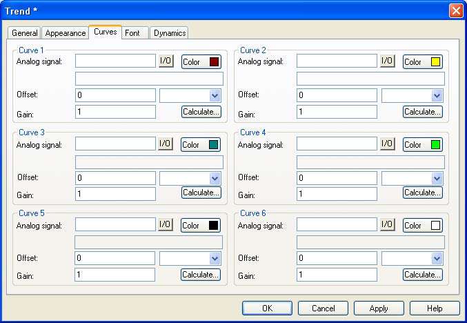
Figure 34 – Curves tab parameters
Table 8 shows description of trend curve parameters which were vital towards the project’s HMI outcome.
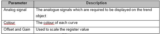
Table8– Trendcurveparameters
After the trend object is being setted, the parameters from the A/D converter to the PLC were successfully implemented as curves. The image below shows the layout on the HMI screen when the motor connected is active.
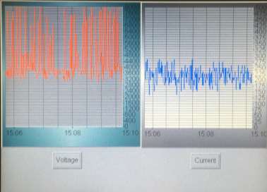
figure 35 – trend function display
The ‘enable sampling signal’ parameter in the general tab was utilized to execute a “show/conceal” signals influence. This was controlled by the buttons named “Voltage” and “Current”. By flipping these buttons, it would either show or conceal the relating signal.
Retrieving Data
Another element of the E-Designer programming that was utilized towards this project was the File exchange Protocol (FTP). This component is a system convention standard that is utilized to exchange documents from a host to an administrator or the other way around. This strategy relies on upon the example interim set for the pattern capacities. This was utilized to effortlessly recover the put away voltage and current computerized values from the plc and store into a Microsoft Office Excel® known configuration (skv). With the goal for this to be finished, the accompanying strides were taken after.
3.4 HardwareAdditions
A new idea was implemented within the hardware of the project, this new idea or concept is about different ways of detecting or monitoring spikes. The concept is focused on a LED illuminating whenever a voltage spike occur.
3.4.1Changesinhardware
In order to make this idea functional, a jk flip flop and a voltage comparator was needed in addition to the circuit. The image below illustrates a connection architecture of the system. It shows the use of a LED.
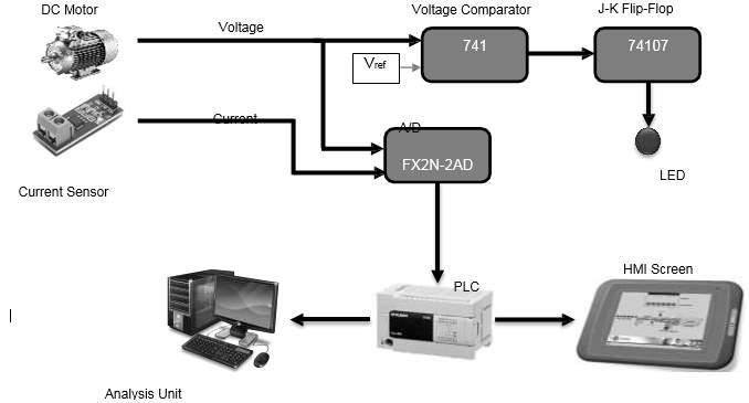
Figure37– Reviseddiagram
3.4.2VoltageComparator
Voltage comparator compares two voltages. The voltage passes through if the input voltage is greater than a supply reference voltage. Voltage comparator used in this project was the LM741 normally used in small application. The image below shows pin connectivity of the OP AMP.
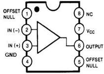
Figure38– LM741OP–AMP
The following setup are ways in which the voltage comparator was connected to the hardware.
¾ OFFSET NULL: NC
¾ IN (-): Vref of 7 volts
¾ IN (+): +V end of motor end
¾ GND: -V
¾ NC: NC
¾ VCC: supply of 9 volts
¾ OUTPUT: input of J-K Flip-Flop
¾ OFFSET NULL: NC
The LED remains on after the LM741 Op-Amp is implemented but due to many voltage spikes produced during the project, the LED was switching on and off quickly. Furthermore, that caused a fast flickering effect which brought in the introduction of a JK flip flop to reduce the amount of ON states for the LED.
3.4.3J-KFlip-Flop
J-K is made up of four NAND gates as seen on the circuit below.
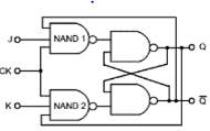
Figure39– BasicJKFlipFlop
The JK flip flop has two inputs which are J and K, two outputs Q and ”NOT Q” which is the inverse of Q. furthermore, this output depends on the clock.
The JK flip flop used was the LM74107 as seen on the diagram below which is a dual flip-flop integrated circuit.
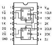
Figure40– Pin connections
Figure 40 also shows the pin connections of the flip-flop and since only the flip-flop was needed, the top flip-flop was used. The implementation setup within the hardware are as follows:
¾ VCC: 4 volts supply
¾ 1CLR: OUTPUT from voltage comparator (pin 6)
¾ 1CK: Clock frequency of 1Hz
¾ 1J: OUTPUT from voltage comparator (pin 6)
¾ 1Q: LED
¾ GND: -V
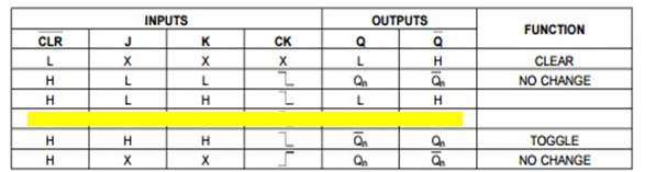 Table9– JKFlip-FlopTruthTable
Table 9 shows the truth table for the J-K flip-flop and defines its functionality. From the table it can be seen that the required function is the same as the region highlighted yellow. In reduction of spikes observed by the LED, a clock with low frequency reduces the number of Q outputs.
3.5 Summary
The main aim of this chapter was to give the readers an idea of the work carried out in the project. It showed procedures of the project which were explained.
The first subsections briefly gave the overview of the entire system. The second part explained the design of the hardware while the third subsection explained the software techniques used to enable the system function. Lastly, the four section gave knowledge on the idea of using a LED to monitor voltage spikes. Next chapter will be discussing the results obtained from the data collected.
4 Result
This chapter is based on the observations gotten from the result s of the system and it also shows the ways at which the data was achieved and analysed. This chapter is divided into two parts, the first part is based on analyses the spikes that occurred by observing a sample of the gathered data. The second part is based on the fast Fourier transform (FFT) analysis performed on the data.
4.1 Spikes Analysis
Spikes analysis explains ways that were used to analyse the obtained data. It elaborates more on the three spikes variations that have gained through the project. Which are voltage, spikes, current and power spikes.
4.1.1 Voltage Spikes
From the table below, we can see the sample of 10 rows obtained from the full length of data shown in appendix B.
The aim of the data analysis is to show the difference between voltages and spikes. The data was collated with a sampling rate of 1.
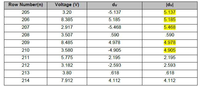 Table 10 – Voltage Spikes
Measuring differences of voltage data was used on the data set to help see deviation intensity between each data value.
Dv is the deviation from previous voltage. Given dV = Vn – Vn-1, an equation can be derived. For example: dv value for row 10 would be: V210 – V209 => 3.580 – 8.485 = -4.905.
| dV |: represents the ABS of dv.
From the previous example, this would be equal to 4.905 and it would also convert values to positive values.
9volts was used to supply voltage through the circuit deviations that are more than half of the supply, that is 4.6v, would be considered as voltage spike. The outcome of this process results to the graph shown below. Any value that is above the red line is considered as voltage spike.
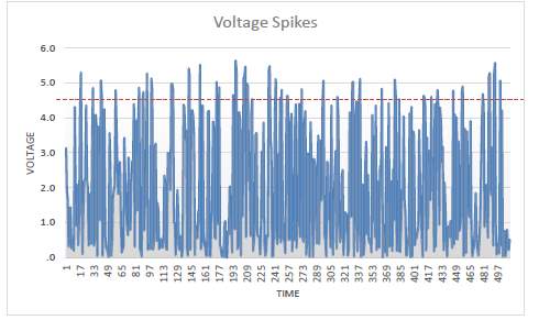
Figure 41 – Voltage Spikes graph
4.1.2 Current Spikes
The sample of 10 rows that were taken from the full length of data seen in appendix B is shown on the table below.
Analysis of the data is to show difference between acceptable currents and spikes.
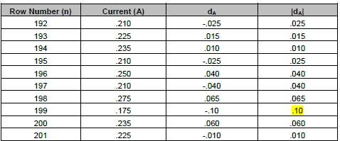
Table 11 – Current Spikes
Measurement of the difference between current data was used on the data set to help see the intensity of deviation between each data value.
dA stands for deviation from the previous voltage, therefore a simple equation can be gotten from dA = An – An-1 in a case that the dA value for row 200 would be A200 – A199 => 0.235 – 0.175 = -0.060.
This converts values to be positive and it would be equal to 0.060 as seen in the earlier example.
Values that are above 0.1A would be considered as current spikes and this method was observed or followed throughout the whole data size to produce the graph see in figure 42. Values above the red lines are considered as current spikes.
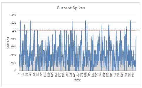
Figure 42 – Current Spike graph
4.1.3 Power Spikes
The table below shows a sample of 10 rows which were taken from the full length of data shown in Appendix B.
the aim of analysing the data is to be able to distinguish between acceptable power values and spikes.
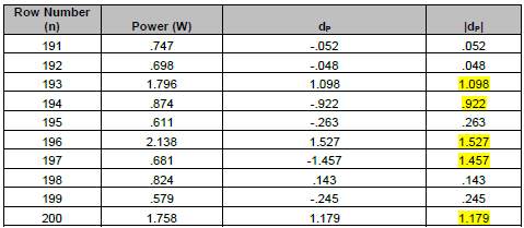
Measurement of the difference between power data was used on the data set to help see the intensity of deviation between each data value.
dp stands for deviation from the previous voltage therefore a simple equation can be gotten from dP = Pn – Pn-1. in a case that the dp value for row 200 would be P200 – P199 => 1.758 – 0.579 = 1.179
| dA |: represents the ABS of dA
This converts values to be positive and it would be equal to 1.179 as seen in the earlier example.
Values that are above 0.9W would be considered as current spikes and this method was observed or followed throughout the whole data size to produce the graph see in figure 44. Values above the red lines are considered as power spike.
Figure43– PowerSpikesgraph
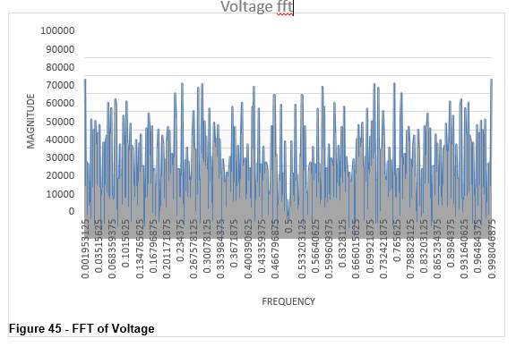
4.2 FastFourierTransformAnalysis
After the data from the plc was stored as a Microsoft Office Excel format, FFT analysis was performed on each data sets; voltage, current and power. This was made possible by the Microsoft Office Excel built-in FFT function.
The purpose of the fast furrier transform analysis is to convert a spectrum from time domain to frequency domain. The “IMABS()” was used to calculate values for each magnitude because the magnitude (Y axis) conversion into frequency domain had values of real and imaginary parts.
Furthermore, the magnitude (x axis) was converted from time to frequency domain using the following equation: FFT freq = n x fs / sa
n for row number starting from 0
fs fro sampling frequency
sa for total number of samples taken.
Lastly, the number of samples had to be a power of 2 in oder for the FFT to be performed.
4.2.1VoltageAnalysis
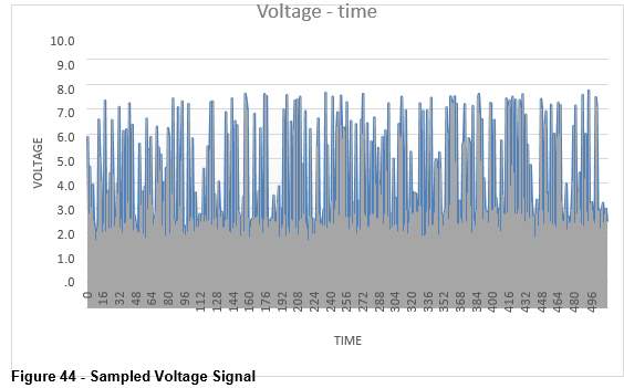
Figure 45 illustrates applied FFT voltage graph:
4.2.2Current Analysis
The following signals are sampled data in time domain
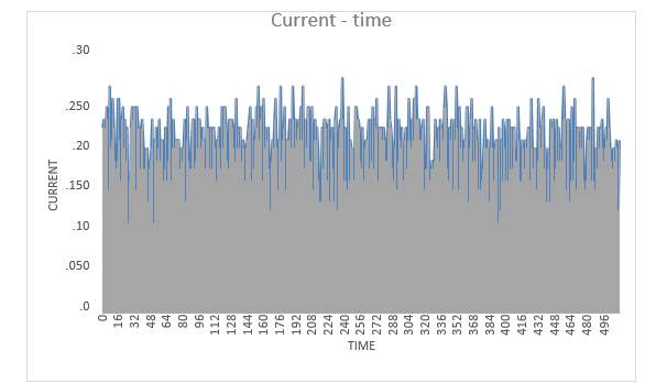
Figure46– SampledCurrentSignal
The following graph was acquired after performing FFT on current values.
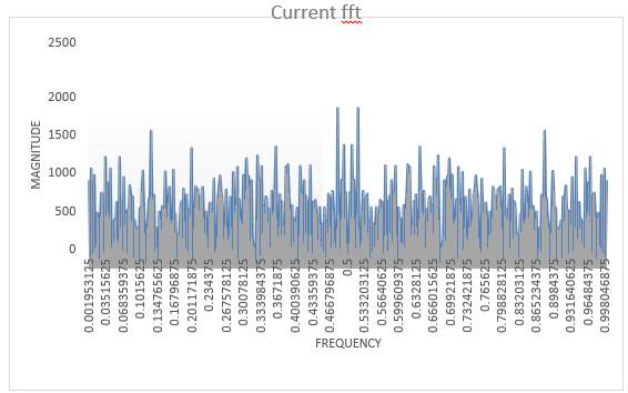
Figure47– FFTofCurrent
4.2.3PowerAnalysis
The graph below illustrates sampled power signal in time domain
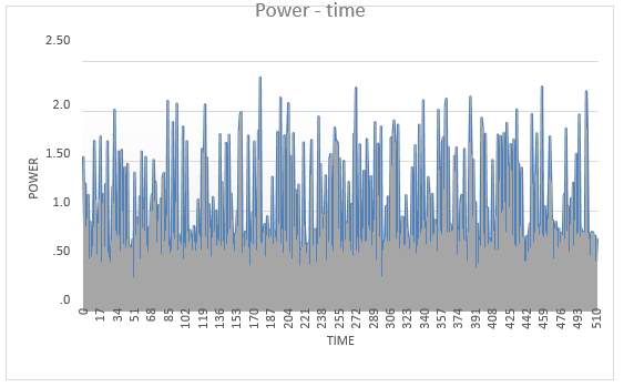
Figure48– SampledPowerSignal
The graph in figure 49 shows the FFT of the power signal
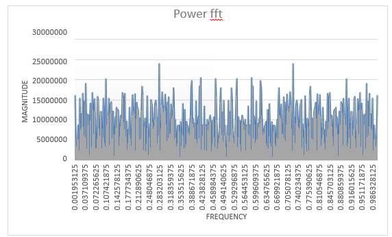
Figure49– FFTof Power
4.2.4Limitations
From the FFT performed on sampled data, the applied sample rate does not allow signals to be analysed correctly and is needed to be increased. Signals analysed by FFT are dcalled ghost signals which means the singnal sample data are reflections of the original signals which are offsets. The true signals can be seen between the 1 second window. Limitationn encountered was due to low resources for the PLC used which caused the inability for data to be obtained and transffered to the computer at a high rate than 1 sample per second.
4.3 Summary
The chaptered was focused on explaining the techniques used in analysing the data and also the limitation encountered during the process.
5 Conclusion
This project was based on a PLC system designed to monitor current and voltage noise in a power supply. The aim of this report is to help discuss techniques and procedures used in achieving the purpose of the project. At the beginning, the subject review section gives overview and background knowledge of the entire project. The report included the structure of the plc based system which was linking a hardware and software implementation to achieve a working system. Some safety measures were also considered in the report when monitoring by proper selection and wiring of the right components.
Furthermore, screen shots of the software implementation is seen on the report and due to lack of time, complete results for the spikes and FFT analysis were not obtained.
From the objectives stated at the beginning of the project, this report proves that all the stages were met, except obtaining complete results due to lack of time.
- Ability to monitor and detect power qualities, focusing primarily on spikes formed in the power line
- Hardware development and design unit to detect and display unwanted signals.
- Using an analogue to digital(A/D) converter to translate the readings coming from the analogue signal in the circuit into digital values.
- Implementing a ladder logic downloading it to the PLC to read the digital data obtained from the circuit by the A/D convertor and storing the data registers.
- Sampling obtained digital values on a displaying them with aid of Human Machine Interface (HMI) screen to monitor the spikes that occur through the system.
- Transferring the data onto Microsoft Office Excel® performing Fast Fourier Transform (FFT) to analyse the data obtained and prove an appropriate sampling rate
- Implementing a voltage comparator and J-K Flip-Flop to develop the hardware unit to use a LED as an indication whenever a spike occurs.
- Hardware Design
From the feasibility report, we could see that the system is capable of monitoring spikes and harmonics in a powerline of a power supply.
Cite This Work
To export a reference to this article please select a referencing stye below:
Related Services
View all


Related Content
All TagsContent relating to: "Engineering"
Engineering is the application of scientific principles and mathematics to designing and building of structures, such as bridges or buildings, roads, machines etc. and includes a range of specialised fields.
Related Articles

DMCA / Removal Request
If you are the original writer of this dissertation and no longer wish to have your work published on the UKDiss.com website then please: