Fabrication and Characterization of Organic Light Emitting Diode (OLED)
Info: 4846 words (19 pages) Dissertation
Published: 27th Oct 2021
Tagged: Electronics
Fabrication and Characterization of Organic Light Emitting Diode (OLED) with Different Concentration of Polyethylenimine Ethoxylated (PEIE) as Electron Transport Layer
Introduction
An organic light emitting diode (OLED) is a solid-state semiconductor device that made up of organic electroluminescent material in order to emits light in response to electric current. The current goal for lightning field is to replace all conventional lightning sources with more power efficient semiconducting light sources [1]. OLED technology has started in 1963 when electroluminescence (EL) in organic semiconductor was reported by Pope et al. [2]. Currently, OLED technology field has been progress rapidly as one of the most promising technologies for display and lightning application which hold a great economic potential [3]. OLED exhibit a lot of advantages compared to semiconductor light emitting diode (LED) such as, thinner, lighter, more flexible, self-emission (do not require backlight), good daylight visibility, wide viewing angle (about 170º), and fast response time (fast refresh rate). Besides that, low voltage, and low power required to light up the OLED which will help to save more energy. As compared to liquid crystal display (LCD) technology, OLED is a self-emissive display which no extra backlight needed, this will reduce number of layers, and reduce the number of process flow in order to make fabrication process easier.
Basically, OLED is made up of 2 to 3 layers of organic films sandwiched between two electrodes on substrate. Conventionally, OLED is fabricated on a glass substrate [3] because of its transparent and supportive properties which allows the light to be visibly emitted through. In common, a transparent indium tin oxide (ITO) anode and a non-transparent reflective metal cathode such as aluminium (Al) are sandwiching the organic thin films. This type of OLED called as bottom-emission OLED (BOLED) [4] where the light emits from the bottom of glass surface. In between, a conductive layer and an emissive layer which are organic molecules or organic polymers purposes of transporting “holes” from anode and transporting “electrons” from cathode respectively. The conduction in OLED is driven by delocalization of π electron. By applying some voltage to turn on the OLED device, the conducting level in organic molecules varied from insulator to conductor. Holes injected from anode into conductive layer through highest occupied molecular orbital (HOMO), while electron injected from cathode into emissive layer (EML) through lowest unoccupied molecular orbital (LUMO) [7]. The electron-hole pair will recombine, form exciton (bound state of electron and hole) [6], and lead to photon emission which produce light in form of electroluminescence.
In this research, the OLED layers are arranged and fabricated in sequence, where glass as substrate, indium tin oxide (ITO) as anode (+), poly[2-methoxy-5-(2-ethylhexyloxy)-1,4-phenylenevinylene] (MEH-PPV) as hole transport layer (HTL), polyethylenimine ethoxylated (PEIE) as electron transport layer (ETL), and aluminium as cathode (-). In advanced of modifying the electron transport performance, PEIE proposed as surface modifier with different concentration due to PEIE having wide range of adaptability, durability, and robustness. Different concentration of PEIE can decrease the work function (WF) of Al by more than 1.0 eV of fixed PEIE’s concentration which founded by A. Falco et al. [8] in order to further improve electron injection from the cathode.
Literature Review
Introduction
These reviews include discussion of fundamental and principle of operation of organic light emitting diode (OLED). Materials and fabrication of OLED are discussed with comparing the result founded by professional researchers. There also brief discussion of OLED’s application, advantages and disadvantages, and comparison between different OLED and other devices. Research for effect of different concentration of poly[2-methoxy-5-(2-ethylhexyloxy)-1,4-phenylenevinylene] (MEH-PPV) and polyethylenimine ethoxylated (PEIE) also been discussed in the final discussion of this literature review.
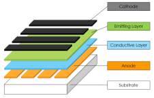
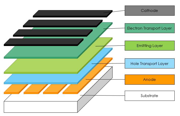
OLED’s Fundamental Structure
The basic structure of OLED is mainly of indium tin oxide (ITO), conductive metal layer, two organic layers (conductive layer and emitting layer), and glass substrate as shown in Figure 2.1 (a). In three organic layers based OLED [6], the single conductive layer is replaced by two more effective conductive layers such as electron transport layer (ETL) and hole transport layer (HTL) which display in Figure 2.1 (b).
 |
 |
| (a) | (b) |
Figure 2.1 (a) Fundamental structure of two layers based OLED, (b) Fundamental structure of three layers based OLED
OLED’s Operation Principle
Electroluminescence (EL) from organic materials was first observed in 1960 by Pope et al. [2], but it has high driving voltage of hundreds volts. The OLED is further improved with proposing two-layer organic layers by Tang et al. [9] in 1987 until having the thickness of ETL and HTL were around 70 nm. Under electrical current supply, holes and electrons are injected from anode into HTL through HOMO and cathode into ETL through LUMO respectively. The electrons and holes are recombined near the HTL/ETL interface, and form excitons which will give out light after recombination. From the EL process in Figure 2.2, the work function of anode should be high to promote holes injection. Inversely, the work function of cathode should be low to promote electrons injection. Typically, work function of ITO is about 4.7 eV which should be as high as possible, followed by MEH-PPV of work function around 5.2 eV as HTL. EML same purpose as ETL for two layer based OLED, PEIE deposited to reduce the work function of Al cathode from 4.2 eV to 3.2 eV.
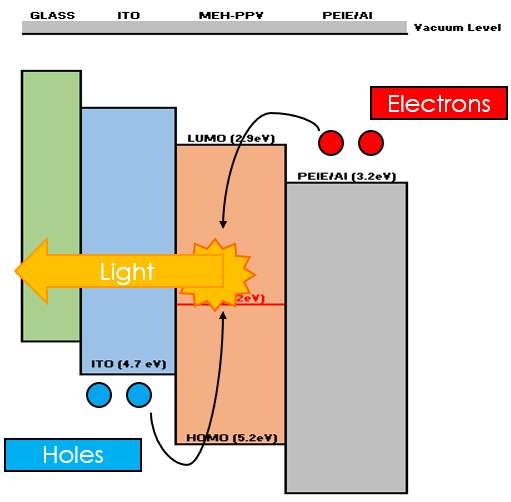
Figure 2.2 Working principle of OLED
OLED’s Materials
Materials are critical factor for both efficiency and lifetime of OLED [6]. Revolutionary improvement of OLED efficiency can be applied by introducing new materials. From the first generation of fluorescent materials until the novel transport and emission layer materials, the efficiency OLED has been grown more than tenfold. Continuous development of OLED materials also allowed devices to operate with a lifetime of hundreds of thousands of hours. Besides, increasing of layers in OLED also helps for carriers’ injection and charge blocking effect from reaching opposite side of OLED.
Substrate
The substrate is used to support OLED. The most common materials for substrate are glass, plastic, and foil which are transparent for the light to emit.
Anode
The anode usually uses highly transparent ITO for light visibility. This material also a good conductor with high work function in order to promote the injection of holes into HOMO level of organic layer. Graphene based anode may be the future conductive anode which exhibit almost same properties as ITO and used to replace current ITO transparent anode [13].
Hole Transport Layer (HTL)
P-type materials are typically chosen as HTL. These material are poly(3,4-ethylenedioxythiophene):poly(styrenesulfonate) (PEDOT:PSS), N,N-diphenyl-N,N-bis(3-methylphenyl)-1,10-biphenyl-4,4-amine (TPD), and N,N-Bis(naphthalen-1-yl)-N,N-bis(phenyl)benzidine (NPB).
Emissive Layer (EML)
The EML is made up of organic plastic molecules. The colour of light produced is depending on the type of organic molecule used for the process. Besides, light produced also depends on the intensity. The more the current applied, the more brighter the light produced due to recombination of electron-hole pairs and form excitons. Most commonly used material is polyfluorene (PFO) from fluorescent dye and phosphorescent dye. Poly[2-methoxy-5-(2-ethyl-hexyloxy)phenylene vinylene] (MEH-PPV) also widely used to produce the light orange-red in colour [14].
Electron Transport Layer (ETL)
N-type materials are typically chosen as ETL. Most common components used are polyethylenimine ethoxylated (PEIE), 2-(4-Biphenyl)-5-(4-tert-butylphenyl)-1,3,4-oxadiazole (PBD), tris(8-quinolinolato) aluminium (Alq3), and 2,9-Dimethyl-4,7-diphenyl-1,10-phenanthroline (BCP).
Cathode
The cathode is deposited with aluminium (Al) in common, but it still depends on the type of OLED used. The cathode can be either transparent or solid metal type, such as barium, calcium, aluminium, gold, and ITO. Conductor with lesser work function will be chosen as cathode in order to improve electron injection.
OLED’s Fabrication Technology
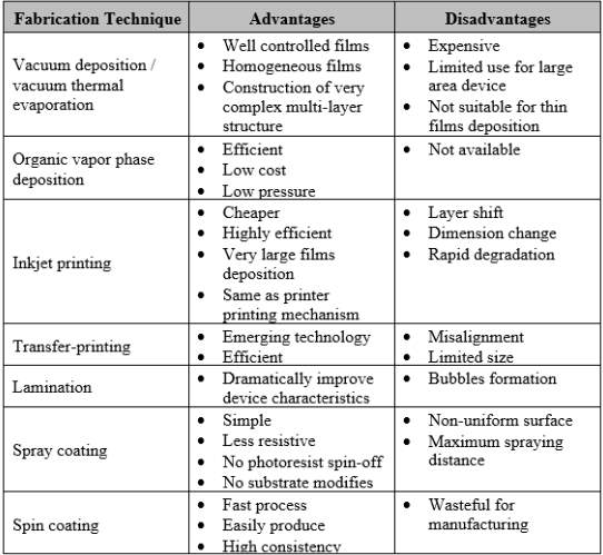
In commercial, the OLED most commonly fabricated using vacuum sublimation which efficiently for the fabrication of advanced multilayer devices in order to match energy level of material used. Currently, many cheaper, high efficient, large area device production, device characteristics improvement technologies provide better solution techniques for OLED’s fabrication. These technologies include vacuum deposition or vacuum thermal evaporation [15], organic vapor phase deposition [6], inkjet printing [15], transfer-printing [6], [16], [17], lamination [18], [19], spray coating [20], [21], and spin coating [1], [22]–[25]. The advantages and disadvantages of each fabrication techniques are summarized in Table 2.1.
Table 2.1 Comparison of fabrication techniques
OLED’s Application
OLEDs are used to make digital displays in most of recent devices. For instances, smart phone displays, computer screens, television screens, car radio, car lightning, and other OLED integrated device units. OLEDs provide high brightness, high contrast in application for visibility and readability under sunlight, low power drain, better device efficiencies, operational stability, and high pixel per inch (PPI). According to Y. Karzazi [6], OLED’s mainly classified into passive-matrix OLED (PMOLED), active-matrix OLED (AMOLED), transparent OLED (TOLED), top-emitting OLED (TEOLED), foldable/flexible OLED (FOLED), and white OLED (WOLED).
 |
 |
| (a) | (b) |
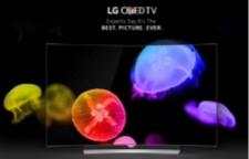
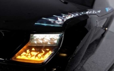
Figure 2.3 (a) Flexible curve OLED TV, (b) White OLED light beam
Comparison of OLED and Other Devices
On the trend of developing display, produced display will be thinner, lighter, flexible and transparent. The differences between organic light emitting diode (OLED), liquid crystal display (LCD), and plasma can be determined through comparison of layers architectures, layers materials, power consumption and devices performances. Figure 2.4 shows the comparison of OLED with LCD and plasma.
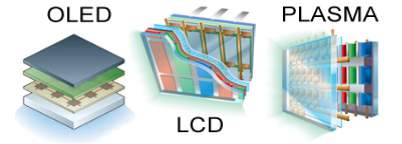
Figure 2.4 Basic structure and architecture of OLED, LCD, Plasma
Organic Light Emitting Diode (OLED)
OLED form from a stack of organic polymers deposited on thin-film transistor (TFT) array without backlight or projection lamp. OLED having the least number of organic polymer layers compared to other devices. OLED does not need to wait for all pixels to fire up in order to respond to signal due to the fast response time and fast switching time in about microseconds. OLED provide the purest colour tone display, better picture quality, high contrast and wide viewing angle (~160º). In future, transparency of OLED displays will reach 100% transparent with thinnest display available (ultra-slim) like a mirror or glass [18]. Power consumption can be dramatically decreased. Manufacturing processes around 6 steps and operation temperature range from 50ºC to 80ºC.
Liquid Crystal Display (LCD)
LCDs are widely used in many electronic products which stand in the mainstream of flat panel displays todays [26]. Two sheets of glass are sandwiching the liquid crystal filled red, green, and blue pixel cells to form a LCD. Voltage is applied on a matrix thin film transistor, the crystals will “untwist” to filter light from the backlight. LCD have the advantages of small volume, light quality, and low power consumption, but it need a backlight to support and light up the display unit. Manufacturing processes steps for LCD was high at about 9 steps and operation temperature range from 0ºC to 100ºC. Inversely, LCD have limited view angle and an average life-span of 3 to 8 years [27].
Plasma
Plasma display has become popular display before with display device uses a gas discharge to transform an electric signal into visible image. Plasma will activate the cell’s coloured phosphor to from image processed. Plasma display panel faces ohmic loss and switching loss while on the sustaining current path [28]. Plasma displays have a superior performance in 3D application due to wide viewing angle availability, high response speed, high dynamic definition, large colour gamut, and high contrast [29].
Effect of Modified Cathode With PEIE
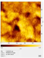
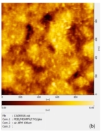
Xiaohui Yang et al. [8] reported 80% ethoxylated polyethylenimine (PEIE) is diluted with 2-methoxyethanol by a factor of 50 and deposited on OLED will increase the luminance of OLED by a factor of ca. 30. The luminance on-set-voltage of OLED with PEIE also reported decreased to ca. 2 V as compared to OLED’s aluminium cathode without PEIE which will have high on-set-voltage of 4 V. The surface root-mean-square (RMS) roughness also improved by 0.2 nm with the implementation of PEIE, the RMS roughness enhanced from 1.1 nm without PEIE in Figure 2.5(a) to 1.3 nm with PEIE in Figure 2.5(b).
 |
 |
| (a) | (b) |
Figure 2.5 Smooth surface with root-mean-square (RMS) roughness of (a) 1.1 nm without PEIE, (b) 1.3 nm with PEIE
Effect of Different Concentration and Spraying Time of PEI/PEIE on Thickness, Roughness and Work Function of OLED using Spray Coating Deposition
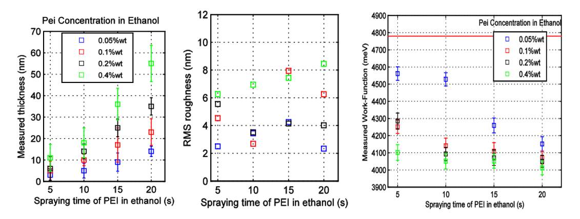
Spray deposition coating [20] is one of the most prominent techniques to obtain easy-to-scale production. Spray coating of Polyethylenimine (PEI) need to follow some important parameters such as nozzle-to-sample distance, heat-plate temperature, atomization pressure, spraying time, choice of solvent, and material concentration. A. Falco et al. [20] reported that PEI concentration of 0.4 %wt in ethanol have the best thin films characteristics at 20 s. The lowest work function found by Falco et al. was 4.0 eV, maximum roughness at 8.5 nm, and maximum thickness of 55 nm as shown in Figure 2.6.
 |
||
| (a) | (b) | (c) |
Figure 2.6 Effect of concentration of PEI in Ethanol on (a) thickness, (b) roughness, and (c) work function with increasing spraying time [20]
Problem Statement
The organic light emitting diode (OLED) is fabricating with few layers of organic material to form electron transport layer, emissive layer, and hole transport layer. Each layer of OLED is fabricating using different material type, thickness and concentration to improve properties such as hole and electron injection, luminance, surface roughness, work function and degradation time of OLED.
Few fabrication methods can be implemented for the fabrication of OLED, such as vacuum deposition or vacuum thermal evaporation (VTE), organic vapor phase deposition (OVPD), inkjet printing, transfer-printing, lamination, spin-coating. The best OLED’s fabrication method need to be chosen for the best material parameters.
Besides, poly[2-methoxy-5-(2-ethylhexyloxy)-1,4-phenylenevinylene] (MEH-PPV) and poly-ethylenimine ethoxylated (PEIE) are suggested as hole transport layer and electron transport layer respectively. MEH-PPV implemented to increase hole injection from anode to MEH-PPV layer. Meanwhile, PEIE also implemented to reduce the work function of cathode about 1.0eV with increasing electron transport from cathode to PEIE layer.
Since MEH-PPV with different concentration has been done in order to improve hole injection, different concentration of PEIE with fixed concentration of MEH-PPV will be implemented to determine electron injection improvement of OLED. I-V and J-V characteristics of OLED may also have improvement with different concentration of PEIE. Work function of cathode may be further reducing more than 1.0eV with different PEIE’s concentration. Hence, different concentration of PEIE need to be produced and to examine the effect of PEIE’s concentration to the OLED’s parameters, luminance, efficiency, and performance which will be the focus of this research work.
Objectives and Scopes
Objectives
To fabricate organic light emitting diode (OLED) with layer orientation of Glass/ITO/MEH-PPV/PEIE/Al using spin-coating fabrication.
To study and improve the performance of organic light emitting diode (OLED) with different concentration of polyethylenimine ethoxylated (PEIE).
To analyse the I-V and J-V characteristics of organic light emitting diode (OLED) with different concentration of polyethylenimine ethoxylated (PEIE).
Scopes
To fabricate the organic light emitting diode (OLED) in sequence of Glass/ITO/MEH-PPV/PEIE/Al using spin-coating fabrication.
To design and pattern the organic light emitting diode (OLED) using lithography process.
To formulate the different solution concentration of polyethylenimine ethoxylated (PEIE).
To identify the effect of different concentration of polyethylenimine ethoxylated (PEIE) to organic light emitting diode (OLED).
To generate the I-V characteristic of organic light emitting diode (OLED) with different concentration of polyethylenimine ethoxylated (PEIE).
To generate the J-V characteristic of organic light emitting diode (OLED) with different concentration of polyethylenimine ethoxylated (PEIE).
To discuss the application of organic light emitting diode (OLED).
To discuss the future improvement of organic light emitting diode (OLED).
Methodology
Generally, OLEDs are fabricated in a class 1000 cleanroom. Clean environment allows OLEDs to be produced with high consistency possible. However, OLEDs relatively tolerant with contaminations like dusts, it is insulating and generally device only stop working when the dust landed on surface [30]. Fabrication steps is discussed from substrate to devices ready for use.
Before fabrication of OLED, materials are prepared. MEH-PPV solution is prepared at concentration of 5mg/ml (Equation 5.1) in toluene solvent due to high conductive, more uniform, less aggregation of active thin films will be produced which reported by N.E.A. Azhar et al. [24]. PEIE solution is prepared with few concentrations, 0.5 %wt, 1.0 %wt, 1.5 %wt, and 2.0 %wt (Equation 5.2), in 2-methoxyethanol solvent.
| weightvolume mg/ml= weight of soluteweight of solution | (Equation 5.1) |
| weight percent (%wt)= weight of soluteweight of solution X 100% | (Equation 5.2) |
Glass with ITO is cleaned in sequence in ultrasonic bath of acetone, isopropanol, detergent, deionized (DI) water, and isopropanol [31]. Glass is dried in vacuum baking oven, and oxygen plasma treatment for 20 minutes. ITO pattern is preparing using masking of Figure 5.1, photolithography, and development of photoresist (PR). Potassium hydroxide (KOH) or sodium hydroxide (NaOH) is implemented to etch PR, and hydrogen chloride (HCl) is deposited to develop ITO.
 |
 |
| (a) | (b) |
 |
 |
| (c) | (d) |
Figure 5.1 OLED’s mask pattern (a) ITO mask, (b)MEH-PPV mask, (c)PEIE mask, (d) Al mask
Organic materials, and metal cathode is deposited following the parameters designed in Figure 5.2. An 80 nm orange-red MEH-PPV solution dip into spin-coater with spin coating speed of 1000rpm for 60 s, followed by 10 nm PEIE diluted with 2-methoxyethanol deposited on ITO glass. OLED is completed by thermal deposition of 160 nm Al. All processes are carried out in dry nitrogen atmosphere.
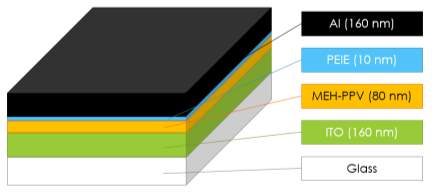
Figure 5.2 OLED’s structures and parameters
Gantt Chart

References
[1] N. Thejo Kalyani and S. J. Dhoble, “Novel materials for fabrication and encapsulation of OLEDs,” Renew. Sustain. Energy Rev., vol. 44, pp. 319–347, 2015.
[2] M. Pope, H. P. Kallmann, and P. Magnante, “Electroluminescence in Organic Crystals,” J. Chem. Phys., vol. 38, no. 8, pp. 2042–2043, Apr. 1963.
[3] M. K. Wei, C. W. Lin, C. C. Yang, Y. W. Kiang, J. H. Lee, and H. Y. Lin, “emission characteristics of organic light-emitting diodes and organic thin-films with planar and corrugated structures,” Int. J. Mol. Sci., vol. 11, no. 4, pp. 1527–1545, 2010.
[4] S. W. Liu, C. C. Lee, C. H. Wang, J. H. Lee, C. T. Chen, and J. K. Wang, “Enhancing performance of planar molecule-based organic light-emitting diodes through deposition-rate optimization: Role of molecular packing,” Chem. Phys. Lett., vol. 474, no. 1–3, pp. 207–211, 2009.
[5] E. Said, Electrolyte-Semiconductor Combinations for Organic Electronic Devices. 2009.
[6] Y. Karzazi, “Organic Light Emitting Diodes: Devices and applications,” Environ. Sci, vol. 5, no. 1, pp. 1–12, 2014.
[7] A. Islam, M. Rabbani, M. H. Bappy, M. A. R. Miah, and N. Sakib, “A review on fabrication process of organic light emitting diodes,” 2013 Int. Conf. Informatics, Electron. Vis., no. May, pp. 1–5, 2013.
[8] X. Yang, R. Wang, C. Fan, G. Li, Z. Xiong, and G. E. Jabbour, “Ethoxylated polyethylenimine as an efficient electron injection layer for conventional and inverted polymer light emitting diodes,” Org. Electron. physics, Mater. Appl., vol. 15, no. 10, pp. 2387–2394, 2014.
[9] S.-C. Dong, L. Xu, and C. W. Tang, “Chemical degradation mechanism of TAPC as hole transport layer in blue phosphorescent OLED,” Org. Electron., vol. 42, pp. 379–386, 2017.
[10] M. G. Helander et al., “Chlorinated indium tin oxide electrodes with high work function for organic device compatibility – SUPP INFO,” Science, vol. 332, no. 6032, pp. 944–7, 2011.
[11] M. R. Krames et al., “Status and future of high-power light-emitting diodes for solid-state lighting,” IEEE/OSA J. Disp. Technol., vol. 3, no. 2, pp. 160–175, 2007.
[12] L. Xiao et al., “Recent progresses on materials for electrophosphorescent organic light-emitting devices,” Advanced Materials, vol. 23, no. 8. pp. 926–952, 2011.
[13] J. Wu et al., “Organic Light-Emitting Diodes on Solution-Processed Graphene Transparent Electrodes,” vol. 4, no. 1, pp. 43–48, 2010.
[14] N. Juhari, W. H. A. Majid, and Z. A. Ibrahim, “Degradation of single layer MEH-PPV Organic Light Emitting Diode (OLED),” IEEE Int. Conf. Semicond. Electron. Proceedings, ICSE, pp. 112–115, 2006.
[15] H. Gorter et al., “Toward inkjet printing of small molecule organic light emitting diodes,” Thin Solid Films, vol. 532, pp. 11–15, 2013.
[16] H. H. Kim et al., “Inverted Quantum Dot Light Emitting Diodes using Polyethylenimine ethoxylated modified ZnO,” Sci. Rep., vol. 5, no. 1, p. 8968, 2015.
[17] S. Choi, Y. Zhou, W. Haske, J. W. Shim, C. Fuentes-Hernandez, and B. Kippelen, “ITO-free large-area flexible organic solar cells with an embedded metal grid,” Org. Electron. physics, Mater. Appl., vol. 17, pp. 349–354, 2015.
[18] C. Y. Lin, N. W. Hu, H. W. Chang, C. Y. Lu, C. Y. Chen, and C. C. Wu, “Efficient transparent small-molecule organic light-emitting devices adopting laminated transparent top electrodes,” Org. Electron. physics, Mater. Appl., vol. 28, pp. 25–30, 2016.
[19] Y. Nishioka, S. Naka, and H. Okada, “MoP-ISCS-129 Semi-transparent OLEDs Fabrication using Lamination Process MoP-ISCS-129,” vol. 7483, no. 2007, pp. 9–10, 2016.
[20] A. Falco, A. M. Zaidi, P. Lugli, and A. Abdellah, “Spray deposition of Polyethylenimine thin films for the fabrication of fully-sprayed organic photodiodes,” Org. Electron. physics, Mater. Appl., vol. 23, pp. 186–192, 2015.
[21] J. Griffin, A. J. Ryan, and D. G. Lidzey, “Solution modification of PEDOT:PSS inks for ultrasonic spray coating,” Org. Electron. physics, Mater. Appl., vol. 41, pp. 245–250, 2017.
[22] A. Alyamani, K. H. Ibnaouf, O. A. Yassin, M. S. Alsalhi, Z. Fekkai, and N. Mustapha, “Spectral, electrical and morphological properties of spin coated MEH-PPV and cresyl violet blended thin films for a light emitting diode,” Optik (Stuttg)., vol. 127, no. 4, pp. 2331–2335, 2016.
[23] J. C. Zhang, Y. L. Jiang, G. D. Zhu, G. P. Ru, and B. Z. Li, “Direct observation of dipole influence induced by a spin coated organic interfacial layer on effective schottky barrier height modulation of Hg/Si contact,” IEEE Electron Device Lett., vol. 35, no. 2, pp. 262–264, 2014.
[24] N. E. A. Azhar, S. S. Shariffudin, I. H. H. Affendi, S. A. H. Alrokayan, H. A. Khan, and M. Rusop, “Characteristic of conjugated polymer MEH-PPV thin films deposited by spin coating method,” 2015 IEEE Student Conf. Res. Dev. SCOReD 2015, no. Cep 2000, pp. 620–624, 2016.
[25] D. Hewidy, A. S. Gadallah, and G. A. Fattah, “Hybrid electroluminescent device based on MEH-PPV and ZnO,” Phys. B Condens. Matter, vol. 507, no. November 2016, pp. 46–50, 2017.
[26] Y. Chen, L. Zhang, and Z. Xu, “Vacuum pyrolysis characteristics and kinetic analysis of liquid crystal from scrap liquid crystal display panels,” J. Hazard. Mater., vol. 327, pp. 55–63, 2017.
[27] F. Cucchiella, I. D’Adamo, S. C. Lenny Koh, and P. Rosa, “Recycling of WEEEs: An economic assessment of present and future e-waste streams,” Renew. Sustain. Energy Rev., vol. 51, pp. 263–272, 2015.
[28] Y. Chung, C. H. Sung, J. H. Kim, S. M. Chae, M. J. Jeon, and B. Kang, “Power-efficient drive circuit for plasma display panel,” Displays, vol. 35, no. 2, pp. 66–73, 2014.
[29] Y. Tu et al., “An ultra-thin shadow mask plasma display panel,” Thin Solid Films, vol. 521, pp. 12–16, 2012.
[30] J. N. Bardsley, “International OLED technology roadmap,” IEEE J. Sel. Top. Quantum Electron., vol. 10, no. 1, pp. 3–9, 2004.
[31] C. Song et al., “The effect of solvent treatment on the buried PEDOT:PSS layer,” Org. Electron. physics, Mater. Appl., vol. 43, pp. 9–14, 2017.
Cite This Work
To export a reference to this article please select a referencing stye below:
Related Services
View all


Related Content
All TagsContent relating to: "Electronics"
Electronics regards the science and technology involved in the development of electrical circuits and electronic devices and equipment that use them.
Related Articles

DMCA / Removal Request
If you are the original writer of this dissertation and no longer wish to have your work published on the UKDiss.com website then please: