Secure Wireless Communication over RF
Info: 19040 words (76 pages) Dissertation
Published: 21st Jan 2022
Tagged: CommunicationsTechnology
CHAPTER 1: INTRODUCTION
1.1 Introduction
This project is about the secure wireless communication over RF. The main advantage of this project is that the data cannot be received until and unless you don’t have receiver code that is compatible to transmitter. At the transmitter, keyboard will be attached to the microcontroller by message entered,and then it is transmitted using radio frequency transmitter. The data which will be entered at the transmitter will also be displayed on LCD for convenient entry. At the receiving end when the encrypted message is received then this message is decrypted by the microcontroller and is displayed on the LCD. The mode of communication that we have used in our project is radio frequency channel. In our project we have used two schemes of data encryption and decryption. One is the Monoalphabetic scheme and the other is Polyalphabetic scheme. The RF modules that we have used for data transmission and reception works at 433MHZ.
To meet the present day technology needs, data transfers at higher speeds are to be achieved which is possible by RF communication. Wireless Data Transfer Using RF Communication Project Report elaborates the working model of RF communication techniques for data transfer. In this we find transmitter section and encoder and decoder are used for the processing of original data.
AT89S52 microcontroller is used for monitoring of the components. The programming part is designed using keil software. The transfer from the pc to controller is done using max 232 cable.
Before transmitting the data, the data will be converted into an unreadable form and will be sent. At the receiving end, the reverse of encryption carries on to get back the original message. Thus the data will be protected in every way by following the encryption and decryption standard formats. Wireless makes this project more flexible. Standard algorithms require software to be installed into the system before actually using them and hardwired connections. The hardware connections and cabling can be completely eliminated in this project.
The most efficient and reliable wireless communication is RF. The RF modules used here are 2.4 GHz UART. The data entered from the PC keyboard is sent to the microcontroller at the transmitter side. The microcontroller converts the data into unreadable form i.e., encrypts the data and then passes the encrypted data to the RF transmitter.
At the receiver end, the RF receiver receives the data from air. The same data is sent to the microcontroller. This microcontroller receives the encrypted data, decrypts the data i.e., finally converts the data into a form suitable for the user to read. This decrypted data can be seen on the receiver PC. Thus, the data is protected while it is transmitted and received between two PCs.
1.2 Project Overview
An embedded system is a combination of software and hardware to perform a dedicated task. Some of the main devices used in embedded products are Microprocessors and Microcontrollers. Microprocessors are commonly referred to as general purpose processors as they simply accept the inputs, process it and give the output. In contrast, a microcontroller not only accepts the data as inputs but also manipulates it, interfaces the data with various devices, controls the data and thus finally gives the result.
1.3 Objective
“The main objective of this project is to ensure security along with better communication”.
CHAPTER 2: EMBEDDED SYSTEMS
2.1 Introduction
An embedded system is a computer system designed to perform one or a few dedicated functions often with real-time computing constraints. It is embedded as part of a complete device often including hardware and mechanical parts. By contrast, a general-purpose computer, such as a personal computer (PC), is designed to be flexible and to meet a wide range of end-user needs. Embedded systems control many devices in common use today.
Embedded systems are controlled by one or more main processing cores that are typically either microcontrollers or digital signal processors (DSP). The key characteristic, however, is being dedicated to handle a particular task, which may require very powerful processors. For example, air traffic control systems may usefully be viewed as embedded, even though they involve mainframe computers and dedicated regional and national networks between airports and radar sites. (Each radar probably includes one or more embedded systems of its own.)
Since the embedded system is dedicated to specific tasks, design engineers can optimize it to reduce the size and cost of the product and increase the reliability and performance. Some embedded systems are mass-produced, benefiting from economies of scale.
Physically embedded systems range from portable devices such as digital watches and MP3 players, to large stationary installations like traffic lights, factory controllers, or the systems controlling nuclear power plants. Complexity varies from low, with a single microcontroller chip, to very high with multiple units, peripherals and networks mounted inside a large chassis or enclosure.
In general, “embedded system” is not a strictly definable term, as most systems have some element of extensibility or programmability. For example, handheld computers share some elements with embedded systems such as the operating systems and microprocessors which power them, but they allow different applications to be loaded and peripherals to be connected. Moreover, even systems which don’t expose programmability as a primary feature generally need to support software updates. On a continuum from “general purpose” to “embedded”, large application systems will have subcomponents at most points even if the system as a whole is “designed to perform one or a few dedicated functions”, and is thus appropriate to call “embedded”. A modern example of embedded system is shown in fig: 2.1.
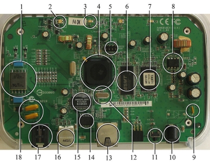
Fig 2.1:A modern example of embedded system
Labeled parts include microprocessor (4), RAM (6), flash memory (7).Embedded systems programming is not like normal PC programming. In many ways, programming for an embedded system is like programming PC 15 years ago. The hardware for the system is usually chosen to make the device as cheap as possible. Spending an extra dollar a unit in order to make things easier to program can cost millions. Hiring a programmer for an extra month is cheap in comparison. This means the programmer must make do with slow processors and low memory, while at the same time battling a need for efficiency not seen in most PC applications. Below is a list of issues specific to the embedded field.
2.1.1 History
In the earliest years of computers in the 1930–40s, computers were sometimes dedicated to a single task, but were far too large and expensive for most kinds of tasks performed by embedded computers of today. Over time however, the concept of programmable controllers evolved from traditional electromechanical sequencers, via solid state devices, to the use of computer technology.
One of the first recognizably modern embedded systems was the Apollo Guidance Computer, developed by Charles Stark Draper at the MIT Instrumentation Laboratory. At the project’s inception, the Apollo guidance computer was considered the riskiest item in the Apollo project as it employed the then newly developed monolithic integrated circuits to reduce the size and weight. An early mass-produced embedded system was the Autonetics D-17 guidance computer for the Minuteman missile, released in 1961. It was built from transistor logic and had a hard disk for main memory. When the Minuteman II went into production in 1966, the D-17 was replaced with a new computer that was the first high-volume use of integrated circuits.
2.1.2 Tools
Embedded development makes up a small fraction of total programming. There’s also a large number of embedded architectures, unlike the PC world where 1 instruction set rules, and the UNIX world where there’s only 3 or 4 major ones. This means that the tools are more expensive. It also means that they’re lowering featured, and less developed. On a major embedded project, at some point you will almost always find a compiler bug of some sort.
Debugging tools are another issue. Since you can’t always run general programs on your embedded processor, you can’t always run a debugger on it. This makes fixing your program difficult. Special hardware such as JTAG ports can overcome this issue in part. However, if you stop on a breakpoint when your system is controlling real world hardware (such as a motor), permanent equipment damage can occur. As a result, people doing embedded programming quickly become masters at using serial IO channels and error message style debugging.
2.1.3 Resources
To save costs, embedded systems frequently have the cheapest processors that can do the job. This means your programs need to be written as efficiently as possible. When dealing with large data sets, issues like memory cache misses that never matter in PC programming can hurt you. Luckily, this won’t happen too often- use reasonably efficient algorithms to start, and optimize only when necessary. Of course, normal profilers won’t work well, due to the same reason debuggers don’t work well.
Memory is also an issue. For the same cost savings reasons, embedded systems usually have the least memory they can get away with. That means their algorithms must be memory efficient (unlike in PC programs, you will frequently sacrifice processor time for memory, rather than the reverse). It also means you can’t afford to leak memory. Embedded applications generally use deterministic memory techniques and avoid the default “new” and “malloc” functions, so that leaks can be found and eliminated more easily. Other resources programmers expect may not even exist. For example, most embedded processors do not have hardware FPUs (Floating-Point Processing Unit). These resources either need to be emulated in software, or avoided altogether.
2.1.4 Real Time Issues
Embedded systems frequently control hardware, and must be able to respond to them in real time. Failure to do so could cause inaccuracy in measurements, or even damage hardware such as motors. This is made even more difficult by the lack of resources available. Almost all embedded systems need to be able to prioritize some tasks over others, and to be able to put off/skip low priority tasks such as UI in favor of high priority tasks like hardware control.
2.2 Need For Embedded Systems
The uses of embedded systems are virtually limitless, because every day new products are introduced to the market that utilizes embedded computers in novel ways. In recent years, hardware such as microprocessors, microcontrollers, and FPGA chips have become much cheaper. So when implementing a new form of control, it’s wiser to just buy the generic chip and write your own custom software for it. Producing a custom-made chip to handle a particular task or set of tasks costs far more time and money. Many embedded computers even come with extensive libraries, so that “writing your own software” becomes a very trivial task indeed. From an implementation viewpoint, there is a major difference between a computer and an embedded system. Embedded systems are often required to provide Real-Time response. The main elements that make embedded systems unique are its reliability and ease in debugging.
2.2.1 Debugging
Embedded debugging may be performed at different levels, depending on the facilities available. From simplest to most sophisticate they can be roughly grouped into the following areas:
- Interactive resident debugging, using the simple shell provided by the embedded operating system (e.g. Forth and Basic)
- External debugging using logging or serial port output to trace operation using either a monitor in flash or using a debug server like the Remedy Debugger which even works for heterogeneous multi core systems.
- An in-circuit debugger (ICD), a hardware device that connects to the microprocessor via a JTAG or Nexus interface. This allows the operation of the microprocessor to be controlled externally, but is typically restricted to specific debugging capabilities in the processor.
- An in-circuit emulator replaces the microprocessor with a simulated equivalent, providing full control over all aspects of the microprocessor.
- A complete emulator provides a simulation of all aspects of the hardware, allowing all of it to be controlled and modified and allowing debugging on a normal PC.
- Unless restricted to external debugging, the programmer can typically load and run software through the tools, view the code running in the processor, and start or stop its operation. The view of the code may be as assembly code or source-code.
Because an embedded system is often composed of a wide variety of elements, the debugging strategy may vary. For instance, debugging a software(and microprocessor) centric embedded system is different from debugging an embedded system where most of the processing is performed by peripherals (DSP, FPGA, co-processor). An increasing number of embedded systems today use more than one single processor core. A common problem with multi-core development is the proper synchronization of software execution. In such a case, the embedded system design may wish to check the data traffic on the busses between the processor cores, which requires very low-level debugging, at signal/bus level, with a logic analyzer, for instance.
2.2.2 Reliability
Embedded systems often reside in machines that are expected to run continuously for years without errors and in some cases recover by them if an error occurs. Therefore the software is usually developed and tested more carefully than that for personal computers, and unreliable mechanical moving parts such as disk drives, switches or buttons are avoided.
Specific reliability issues may include:
- The system cannot safely be shut down for repair, or it is too inaccessible to repair. Examples include space systems, undersea cables, navigational beacons, bore-hole systems, and automobiles.
- The system must be kept running for safety reasons. “Limp modes” are less tolerable. Often backup s are selected by an operator. Examples include aircraft navigation, reactor control systems, safety-critical chemical factory controls, train signals, engines on single-engine aircraft.
- The system will lose large amounts of money when shut down: Telephone switches, factory controls, bridge and elevator controls, funds transfer and market making, automated sales and service.
A variety of techniques are used, sometimes in combination, to recover from errors—both software bugs such as memory leaks, and also soft errors in the hardware:
- Watchdog timer that resets the computer unless the software periodically notifies the watchdog
- Subsystems with redundant spares that can be switched over to software “limp modes” that provide partial function
- Designing with a Trusted Computing Base (TCB) architecture[6] ensures a highly secure & reliable system environment
- An Embedded Hypervisor is able to provide secure encapsulation for any subsystem component, so that a compromised software component cannot interfere with other subsystems, or privileged-level system software. This encapsulation keeps faults from propagating from one subsystem to another, improving reliability. This may also allow a subsystem to be automatically shut down and restarted on fault detection.
- Immunity Aware Programming
2.3 Explanation of Embedded Systems
2.3.1 Software Architecture
There are several different types of software architecture in common use.
Simple Control Loop:
In this design, the software simply has a loop. The loop calls subroutines, each of which manages a part of the hardware or software.
Interrupt Controlled System:
Some embedded systems are predominantly interrupt controlled. This means that tasks performed by the system are triggered by different kinds of events. An interrupt could be generated for example by a timer in a predefined frequency, or by a serial port controller receiving a byte. These kinds of systems are used if event handlers need low latency and the event handlers are short and simple.
Usually these kinds of systems run a simple task in a main loop also, but this task is not very sensitive to unexpected delays. Sometimes the interrupt handler will add longer tasks to a queue structure. Later, after the interrupt handler has finished, these tasks are executed by the main loop. This method brings the system close to a multitasking kernel with discrete processes.
Cooperative Multitasking:
A non-preemptive multitasking system is very similar to the simple control loop scheme, except that the loop is hidden in an API. The programmer defines a series of tasks, and each task gets its own environment to “run” in. When a task is idle, it calls an idle routine, usually called “pause”, “wait”, “yield”, “nop” (stands for no operation), etc.The advantages and disadvantages are very similar to the control loop, except that adding new software is easier, by simply writing a new task, or adding to the queue-interpreter.
Primitive Multitasking:
In this type of system, a low-level piece of code switches between tasks or threads based on a timer (connected to an interrupt). This is the level at which the system is generally considered to have an “operating system” kernel. Depending on how much functionality is required, it introduces more or less of the complexities of managing multiple tasks running conceptually in parallel.
As any code can potentially damage the data of another task (except in larger systems using an MMU) programs must be carefully designed and tested, and access to shared data must be controlled by some synchronization strategy, such as message queues, semaphores or a non-blocking synchronization scheme.
Because of these complexities, it is common for organizations to buy a real-time operating system, allowing the application programmers to concentrate on device functionality rather than operating system services, at least for large systems; smaller systems often cannot afford the overhead associated with a generic real time system, due to limitations regarding memory size, performance, and/or battery life.
Microkernels And Exokernels:
A microkernel is a logical step up from a real-time OS. The usual arrangement is that the operating system kernel allocates memory and switches the CPU to different threads of execution. User mode processes implement major functions such as file systems, network interfaces, etc.
In general, microkernels succeed when the task switching and intertask communication is fast, and fail when they are slow. Exokernels communicate efficiently by normal subroutine calls. The hardware and all the software in the system are available to, and extensible by application programmers. Based on performance, functionality, requirement the embedded systems are divided into three categories:
2.3.2 Stand Alone Embedded System
These systems takes the input in the form of electrical signals from transducers or commands from human beings such as pressing of a button etc.., process them and produces desired output. This entire process of taking input, processing it and giving output is done in standalone mode. Such embedded systems comes under stand alone embedded systems
Eg: microwave oven, air conditioner etc..
2.3.3 Real-time embedded systems
Embedded systems which are used to perform a specific task or operation in a specific time period those systems are called as real-time embedded systems. There are two types of real-time embedded systems.
Hard Real-time embedded systems:
These embedded systems follow an absolute dead line time period i.e.., if the tasking is not done in a particular time period then there is a cause of damage to the entire equipment.
Eg: consider a system in which we have to open a valve within 30 milliseconds. If this valve is not opened in 30 ms this may cause damage to the entire equipment. So in such cases we use embedded systems for doing automatic operations.
Soft Real Time embedded systems:
Eg: Consider a TV remote control system, if the remote control takes a few milliseconds delay it will not cause damage either to the TV or to the remote control. These systems which will not cause damage when they are not operated at considerable time period those systems comes under soft real-time embedded systems.
2.3.4 Network communication embedded systems
A wide range network interfacing communication is provided by using embedded systems.
Eg:
Consider a web camera that is connected to the computer with internet can be used to spread communication like sending pictures, images, videos etc.., to another computer with internet connection throughout anywhere in the world.
Consider a web camera that is connected at the door lock.
Whenever a person comes near the door, it captures the image of a person and sends to the desktop of your computer which is connected to internet. This gives an alerting message with image on to the desktop of your computer, and then you can open the door lock just by clicking the mouse. Fig: 2.2 show the network communications in embedded systems.
Fig 2.2: Network communication embedded systems
2.3.5 Different types of processing units
The central processing unit (c.p.u) can be any one of the following microprocessor, microcontroller, digital signal processing.
- Among these Microcontroller is of low cost processor and one of the main advantage of microcontrollers is, the components such as memory, serial communication interfaces, analog to digital converters etc.., all these are built on a single chip. The numbers of external components that are connected to it are very less according to the application.
- Microprocessors are more powerful than microcontrollers. They are used in major applications with a number of tasking requirements. But the microprocessor requires many external components like memory, serial communication, hard disk, input output ports etc.., so the power consumption is also very high when compared to microcontrollers.
- Digital signal processing is used mainly for the applications that particularly involved with processing of signals
2.4 APPLICATIONS OF EMBEDDED SYSTEMS
2.4.1 Consumer applications
At home we use a number of embedded systems which include microwave oven, remote control, vcd players, dvd players, camera etc….

Fig 2.4.1: Automatic coffee makes equipment
2.4.2 Office automation
We use systems like fax machine, modem, printer etc…
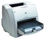
Fig 2.4.2: Fax machine
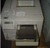
Fig 2.4.3: Printing machine
2.4.3. Industrial automation
Today a lot of industries are using embedded systems for process control. In industries we design the embedded systems to perform a specific operation like monitoring temperature, pressure, humidity ,voltage, current etc.., and basing on these monitored levels we do control other devices, we can send information to a centralized monitoring station.

Fig 2.4.4: Robot
In critical industries where human presence is avoided there we can use robots which are programmed to do a specific operation.
2.4.5 Computer networking
Embedded systems are used as bridges routers etc..
Fig 2.4.5: Computer networking
2.4.6 Tele communications
Cell phones, web cameras etc.

Fig 2.4.6: Cell Phone
Fig 2.4.7: Web camera
CHAPTER 3: HARDWARE DESCRIPTION
3.1 Introduction
In this chapter the block diagram of the project and design aspect of independent modules are considered. Block diagram is shown in fig: 3.1.1:
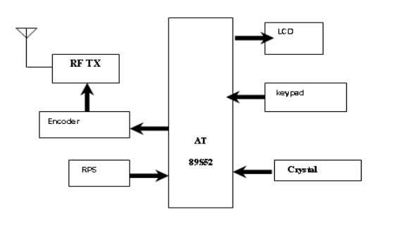
Fig 3.1.1 Block diagram of transmitter
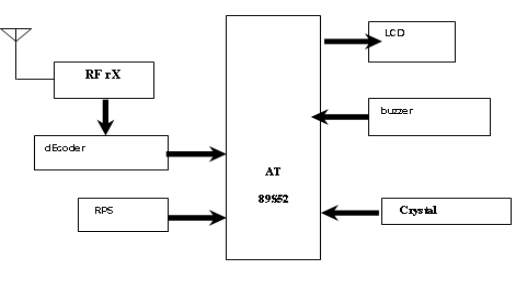
Fig 3.1.2 Block diagram of receiver
The main blocks of this project are:
- Micro controller (AT89S52)
- Reset button
- Crystal oscillator
- Regulated power supply (RPS)
- Led indicator
- Encoder
- Decoder
- RF Transmitter
- RF Receiver
- Keypad
- LCD with driver
- Buzzer
3.2 Micro controller
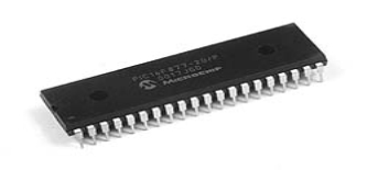
Fig: 3.2 Microcontrollers
3.2.1 Introduction to Microcontrollers
Circumstances that we find ourselves in today in the field of microcontrollers had their beginnings in the development of technology of integrated circuits. This development has made it possible to store hundreds of thousands of transistors into one chip. That was a prerequisite for production of microprocessors, and the first computers were made by adding external peripherals such as memory, input-output lines, timers and other. Further increasing of the volume of the package resulted in creation of integrated circuits. These integrated circuits contained both processor and peripherals. That is how the first chip containing a microcomputer, or what would later be known as a microcontroller came about.
Microprocessors and microcontrollers are widely used in embedded systems products. Microcontroller is a programmable device. A microcontroller has a CPU in addition to a fixed amount of RAM, ROM, I/O ports and a timer embedded all on a single chip. The fixed amount of on-chip ROM, RAM and number of I/O ports in microcontrollers makes them ideal for many applications in which cost and space are critical.
Introduction to AT89S52 Microcontroller:
In this project we interfaced AT89S52 microcontroller with LCD,RF Transmitter, RF Receiver. The AT89S52 is 40 pin IC packaged in DIP package. It is derivative of 8051, from Atmel.
AT89S52 Microcontroller is the heart of the circuit as it controls all the functions of the system. A microcontroller is a single chip that contains the processor ( the CPU), non- volatile memory for the program (ROM or Flash), volatile memory for input and output (RAM), a clock and an I/O control unit. Also called a “Computer on a Chip”.
AT89S52 is an 8-bit high performance microcontroller with low power consumption.
AT89S52 is based on CISC architecture. Most of the instructions execute in one machine cycle.
AT89S52 can work on a maximum frequency of 12MHz.
AT89S52 has 8KB programmable flash memory, static RAM of 256B. It is a 40 pin microcontroller. There are 32 I/O (input/output) lines which are divided into four 8-bit ports designated as P1, P2, P3 and P0.
ATmega32 has various in-built peripherals like UART, TIMERs. Each I/O pin has an alternative task related to in-built peripherals.
PIN DIAGRAM OF AT89S52
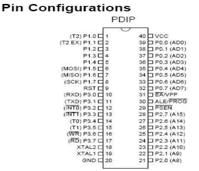
Fig 3.2 .1: Pin Diagram of AT89S52
Pin Description
- Compatible with MCS-51® Products
- 8K Bytes of In-System Programmable (ISP) Flash Memory
- Endurance: 1000 Write/Erase Cycles
- 4.0V to 5.5V Operating Range
- Fully Static Operation: 0 Hz to 33 MHz
- Three-level Program Memory Lock
- 256 x 8-bit Internal RAM
- 32 Programmable I/O Lines
- Three 16-bit Timer/Counters
- Eight Interrupt Sources
- Full Duplex UART Serial Channel
- Low-power Idle and Power-down Modes
- Interrupt Recovery from Power-down Mode
- Watchdog Timer
- Dual Data Pointer
- Power-off Flag
- VCC
- Supply voltage.
- GND
Port 0
Port 0 is an 8-bit open drain bidirectional I/O port. As an output port, each pin can sink eight TTL inputs. When 1s are written to port 0 pins, the pins can be used as high impedance inputs. Port 0 can also be configured to be the multiplexed low order address/data bus during accesses to external program and data memory. In this mode, P0 has internal pullups. Port 0 also receives the code bytes during Flash programming and outputs the code bytes during program verification. External pullups are required during program verification.
Port 1
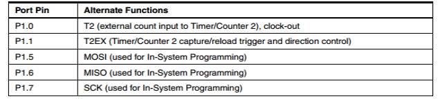
Port 1 is an 8-bit bidirectional I/O port with internal pullups. The Port 1 output buffers can sink/source four TTL inputs. When 1s are written to Port 1 pins, they are pulled high by the internal pullups and can be used as inputs. As inputs, Port 1 pins that are externally being pulled low will source current (IIL) because of the internal pullups. In addition, P1.0 and P1.1 can be configured to be the timer/counter 2 external count input (P1.0/T2) and the timer/counter 2 trigger input (P1.1/T2EX), respectively, as shown in the following table.
Port 1 also receives the low-order address bytes during Flash programming and verification.
Port 2
Port 2 is an 8-bit bidirectional I/O port with internal pullups. The Port 2 output buffers can sink/source four TTL inputs. When 1s are written to Port 2 pins, they are pulled high by the internal pullups and can be used as inputs. As inputs, Port 2 pins that are externally being pulled low will source current (IIL) because of the internal pullups. Port 2 emits the high-order address byte during fetches from external program memory and during accesses to external data memory that use 16-bit addresses (MOVX @ DPTR). In this application, Port 2 uses strong internal pull-ups when emitting 1s. During accesses to external data memory that use 8-bit addresses (MOVX @ RI), Port 2 emits the contents of the P2 Special Function Register. Port 2 also receives the high-order address bits and some control signals during Flash programming and verification.
Port 3
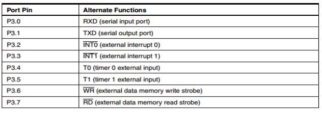
Port 3 is an 8-bit bidirectional I/O port with internal pullups. The Port 3 output buffers can sink/source four TTL inputs. When 1s are written to Port 3 pins, they are pulled high by the internal pullups and can be used as inputs. As inputs, Port 3 pins that are externally being pulled low will source current (IIL) because of the pullups. Port 3 also serves the functions of various special features of the AT89S52, as shown in the following table. Port 3 also receives some control signals for Flash programming and verification.
RST
Reset input. A high on this pin for two machine cycles while the oscillator is running resets the device. This pin drives High for 96 oscillator periods after the Watchdog times out. The DISRTO bit in SFR AUXR (address 8EH) can be used to disable this feature. In the default state of bit DISRTO, the RESET HIGH out feature is enabled.
ALE/PROG
Address Latch Enable (ALE) is an output pulse for latching the low byte of the address during accesses to external memory. This pin is also the program pulse input (PROG) during Flash programming. In normal operation, ALE is emitted at a constant rate of 1/6 the oscillator frequency and may be used for external
timing or clocking purposes. Note, however, that one ALE pulse is skipped during each access to external data memory. If desired, ALE operation can be disabled by setting bit 0 of SFR location 8EH. With the bit set, ALE is active only during a MOVX or MOVC instruction. Otherwise, the pin is weakly pulled high. Setting the ALE-disable bit has no effect if the microcontroller is in external execution mode.
PSEN
Program Store Enable (PSEN) is the read strobe to external program memory. When the AT89S52 is executing code from external program memory, PSEN is activated twice each machine cycle, except that two PSEN activations are skipped during each access to external data memory.
EA/VPP
External Access Enable. EA must be strapped to GND in order to enable the device to fetch code from external program memory locations starting at 0000H up to FFFFH. Note, however, that if lock bit 1 is programmed, EA will be internally latched on reset. EA should be strapped to VCC for internal program executions. This pin also receives the 12-volt programming enable voltage (VPP) during Flash programming.
XTAL1
Input to the inverting oscillator amplifier and input to the internal clock operating circuit.
XTAL2
Output from inverting oscillator amplifier.
3.3 REGULATED POWER SUPPLY
3.3.1 Introduction
Power supply is a supply of electrical power. A device or system that supplies electrical or other types of energy to an output load or group of loads is called a power supply unit or PSU. The term is most commonly applied to electrical energy supplies, less often to mechanical ones, and rarely to others.
A power supply may include a power distribution system as well as primary or secondary sources of energy such as
- Conversion of one form of electrical power to another desired form and voltage, typically involving converting AC line voltage to a well-regulated lower-voltage DC for electronic devices. Low voltage, low power DC power supply units are commonly integrated with the devices they supply, such as computers and household electronics.
- Batteries.
- Chemical fuel cells and other forms of energy storage systems.
- Solar power.
- Generators or alternators.
3.3.2 Block Diagram
REGULATED POWER SUPPLY
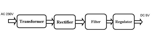
Fig 3.3.2 Regulated Power Supply
The basic circuit diagram of a regulated power supply (DC O/P) with led connected as load is shown in fig: 3.3.3.
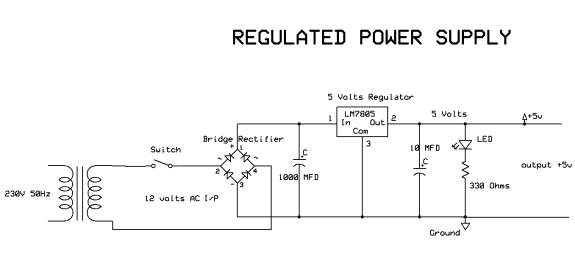
Fig 3.3.3 Circuit diagram of Regulated Power Supply with Led connection
The components mainly used in above figure are
- 230V AC MAINS
- TRANSFORMER
- BRIDGE RECTIFIER(DIODES)
- CAPACITOR
- VOLTAGE REGULATOR(IC 7805)
- RESISTOR
- LED(LIGHT EMITTING DIODE)
The detailed explanation of each and every component mentioned above is as follows:
Transformation:
The process of transforming energy from one device to another is called transformation. For transforming energy we use transformers.
Transformers:
A transformer is a device that transfers electrical energy from one circuit to another through inductively coupled conductors without changing its frequency. A varying current in the first or primary winding creates a varying magnetic flux in the transformer’s core, and thus a varying magnetic field through the secondary winding. This varying magnetic field induces a varying electromotive force (EMF) or “voltage” in the secondary winding. This effect is called mutual induction.
If a load is connected to the secondary, an electric current will flow in the secondary winding and electrical energy will be transferred from the primary circuit through the transformer to the load. This field is made up from lines of force and has the same shape as a bar magnet.
If the current is increased, the lines of force move outwards from the coil. If the current is reduced, the lines of force move inwards.
If another coil is placed adjacent to the first coil then, as the field moves out or in, the moving lines of force will “cut” the turns of the second coil. As it does this, a voltage is induced in the second coil. With the 50 Hz AC mains supply, this will happen 50 times a second. This is called MUTUAL INDUCTION and forms the basis of the transformer.
The input coil is called the PRIMARY WINDING; the output coil is the SECONDARY WINDING. Fig: 3.3.4 shows step-down transformer.
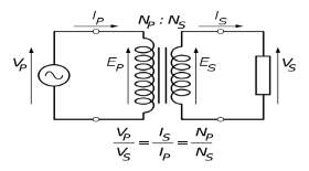
Fig 3.3.4: Step-Down Transformer
The voltage induced in the secondary is determined by the TURNS RATIO.
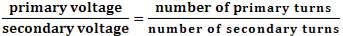
For example, if the secondary has half the primary turns; the secondary will have half the primary voltage.
Another example is if the primary has 5000 turns and the secondary has 500 turns, then the turn’s ratio is 10:1.
If the primary voltage is 240 volts then the secondary voltage will be x 10 smaller = 24 volts. Assuming a perfect transformer, the power provided by the primary must equal the power taken by a load on the secondary. If a 24-watt lamp is connected across a 24 volt secondary, then the primary must supply 24 watts.
To aid magnetic coupling between primary and secondary, the coils are wound on a metal CORE. Since the primary would induce power, called EDDY CURRENTS, into this core, the core is LAMINATED. This means that it is made up from metal sheets insulated from each other. Transformers to work at higher frequencies have an iron dust core or no core at all.
Note that the transformer only works on AC, which has a constantly changing current and moving field. DC has a steady current and therefore a steady field and there would be no induction.
Some transformers have an electrostatic screen between primary and secondary. This is to prevent some types of interference being fed from the equipment down into the mains supply, or in the other direction. Transformers are sometimes used for IMPEDANCE MATCHING.
We can use the transformers as step up or step down.
Step Up transformer:
In case of step up transformer, primary windings are every less compared to secondary winding. Because of having more turns secondary winding accepts more energy, and it releases more voltage at the output side.
Step down transformer:
Incase of step down transformer, Primary winding induces more flux than the secondary winding, and secondary winding is having less number of turns because of that it accepts less number of flux, and releases less amount of voltage.
Battery power supply:
A battery is a type of linear power supply that offers benefits that traditional line-operated power supplies lack: mobility, portability and reliability. A battery consists of multiple electrochemical cells connected to provide the voltage desired. Fig: 3.3.5 shows Hi-Watt 9V battery
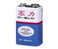
Fig 3.3.5: Hi-Watt 9V Battery
The most commonly used dry-cell battery is the carbon-zinc dry cell battery. Dry-cell batteries are made by stacking a carbon plate, a layer of electrolyte paste, and a zinc plate alternately until the desired total voltage is achieved. The most common dry-cell batteries have one of the following voltages: 1.5, 3, 6, 9, 22.5, 45, and 90. During the discharge of a carbon-zinc battery, the zinc metal is converted to a zinc salt in the electrolyte, and magnesium dioxide is reduced at the carbon electrode. These actions establish a voltage of approximately 1.5 V.
The lead-acid storage battery may be used. This battery is rechargeable; it consists of lead and lead/dioxide electrodes which are immersed in sulfuric acid. When fully charged, this type of battery has a 2.06-2.14 V potential (A 12 volt car battery uses 6 cells in series). During discharge, the lead is converted to lead sulfate and the sulfuric acid is converted to water. When the battery is charging, the lead sulfate is converted back to lead and lead dioxide A nickel-cadmium battery has become more popular in recent years. This battery cell is completely sealed and rechargeable. The electrolyte is not involved in the electrode reaction, making the voltage constant over the span of the batteries long service life. During the charging process, nickel oxide is oxidized to its higher oxidation state and cadmium oxide is reduced. The nickel-cadmium batteries have many benefits. They can be stored both charged and uncharged. They have a long service life, high current availabilities, constant voltage, and the ability to be recharged. Fig: 3.3.6 shows pencil battery of 1.5V.
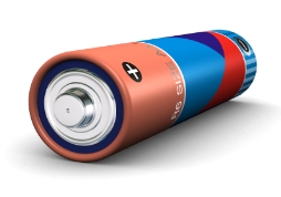
Fig 3.3.6: Pencil Battery of 1.5V
Rectification:
The process of converting an alternating current to a pulsating direct current is called as rectification. For rectification purpose we use rectifiers.
Rectifiers:
A rectifier is an electrical device that converts alternating current (AC) to direct current (DC), a process known as rectification. Rectifiers have many uses including as components of power supplies and as detectors of radio signals. Rectifiers may be made of solid-state diodes, vacuum tube diodes, mercury arc valves, and other components.
A device that it can perform the opposite function (converting DC to AC) is known as an inverter.
When only one diode is used to rectify AC (by blocking the negative or positive portion of the waveform), the difference between the term diode and the term rectifier is merely one of usage, i.e., the term rectifier describes a diode that is being used to convert AC to DC. Almost all rectifiers comprise a number of diodes in a specific arrangement for more efficiently converting AC to DC than is possible with only one diode. Before the development of silicon semiconductor rectifiers, vacuum tube diodes and copper (I) oxide or selenium rectifier stacks were used.
Bridge full wave rectifier:
The Bridge rectifier circuit is shown in fig: 3.3.7, which converts an ac voltage to dc voltage using both half cycles of the input ac voltage. The Bridge rectifier circuit is shown in the figure. The circuit has four diodes connected to form a bridge. The ac input voltage is applied to the diagonally opposite ends of the bridge. The load resistance is connected between the other two ends of the bridge.
For the positive half cycle of the input ac voltage, diodes D1 and D3 conduct, whereas diodes D2 and D4 remain in the OFF state. The conducting diodes will be in series with the load resistance RL and hence the load current flows through RL.
For the negative half cycle of the input ac voltage, diodes D2 and D4 conduct whereas, D1 and D3 remain OFF. The conducting diodes D2 and D4 will be in series with the load resistance RL and hence the current flows through RL in the same direction as in the previous half cycle. Thus a bi-directional wave is converted into a unidirectional wave.
Input Output
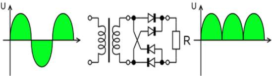
Fig 3.3.7: Bridge rectifier: a full-wave rectifier using 4 diodes
DB107:
Now -a -days Bridge rectifier is available in IC with a number of DB107. In our project we are using an IC in place of bridge rectifier. The picture of DB 107 is shown in fig: 3.3.8.
Features:
- Good for automation insertion
- Surge overload rating – 30 amperes peak
- Ideal for printed circuit board
- Reliable low cost construction utilizing molded
- Glass passivated device
- Polarity symbols molded on body
- Mounting position: Any
- Weight: 1.0 gram
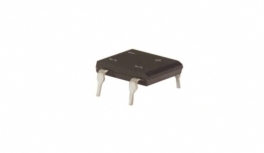
Fig 3.3.8: DB107
Filtration:
The process of converting a pulsating direct current to a pure direct current using filters is called as filtration.
Filters:
Electronic filters are electronic circuits, which perform signal-processing functions, specifically to remove unwanted frequency components from the signal, to enhance wanted ones.
Introduction to Capacitors:
The Capacitor or sometimes referred to as a Condenser is a passive device, and one which stores energy in the form of an electrostatic field which produces a potential (static voltage) across its plates. In its basic form a capacitor consists of two parallel conductive plates that are not connected but are electrically separated either by air or by an insulating material called the Dielectric. When a voltage is applied to these plates, a current flows charging up the plates with electrons giving one plate a positive charge and the other plate an equal and opposite negative charge this flow of electrons to the plates is known as the Charging Current and continues to flow until the voltage across the plates (and hence the capacitor) is equal to the applied voltage Vcc. At this point the capacitor is said to be fully charged and this is illustrated below. The construction of capacitor and an electrolytic capacitor are shown in figures 3.3.9 and 3.3.10 respectively.
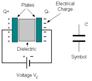
Fig 3.3.9: Construction Of a Capacitor
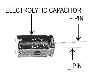
Fig 3.3.10: Electrolytic Capacitor
Units of Capacitance:
Microfarad (μF) 1μF = 1/1,000,000 = 0.000001 = 10-6 F
Nanofarad (nF) 1nF = 1/1,000,000,000 = 0.000000001 = 10-9 F
Pico farad (pF) 1pF = 1/1,000,000,000,000 = 0.000000000001 = 10-12 F
Operation of Capacitor:
Think of water flowing through a pipe. If we imagine a capacitor as being a storage tank with an inlet and an outlet pipe, it is possible to show approximately how an electronic capacitor works.
First, let’s consider the case of a “coupling capacitor” where the capacitor is used to connect a signal from one part of a circuit to another but without allowing any direct current to flow.
 |
If the current flow is alternating between zero and a maximum, our “storage tank” capacitor will allow the current waves to pass through. |
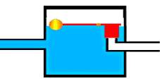 |
However, if there is a steady current, only the initial short burst will flow until the “floating ball valve” closes and stops further flow. |
So a coupling capacitor allows “alternating current” to pass through because the ball valve doesn’t get a chance to close as the waves go up and down. However, a steady current quickly fills the tank so that all flow stops.
A capacitor will pass alternating current but (apart from an initial surge) it will not pass d.c.
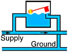 |
Where a capacitor is used to decouple a circuit, the effect is to “smooth out ripples”. Any ripples, waves or pulses of current are passed to ground while d.c. Flows smoothly. |
Regulation:
The process of converting a varying voltage to a constant regulated voltage is called as regulation. For the process of regulation we use voltage regulators.
Voltage Regulator:
A voltage regulator (also called a ‘regulator’) with only three terminals appears to be a simple device, but it is in fact a very complex integrated circuit. It converts a varying input voltage into a constant ‘regulated’ output voltage. Voltage Regulators are available in a variety of outputs like 5V, 6V, 9V, 12V and 15V. The LM78XX series of voltage regulators are designed for positive input. For applications requiring negative input, the LM79XX series is used. Using a pair of ‘voltage-divider’ resistors can increase the output voltage of a regulator circuit.
It is not possible to obtain a voltage lower than the stated rating. You cannot use a 12V regulator to make a 5V power supply. Voltage regulators are very robust. These can withstand over-current draw due to short circuits and also over-heating. In both cases, the regulator will cut off before any damage occurs. The only way to destroy a regulator is to apply reverse voltage to its input. Reverse polarity destroys the regulator almost instantly. Fig: 3.3.11 shows voltage regulator.
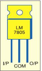
Fig 3.3.11: Voltage Regulator
Resistors:
A resistor is a two-terminal electronic component that produces a voltage across its terminals that is proportional to the electric current passing through it in accordance with Ohm’s law:
V = IR
Resistors are elements of electrical networks and electronic circuits and are ubiquitous in most electronic equipment. Practical resistors can be made of various compounds and films, as well as resistance wire (wire made of a high-resistivity alloy, such as nickel/chrome).
The primary characteristics of a resistor are the resistance, the tolerance, maximum working voltage and the power rating. Other characteristics include temperature coefficient, noise, and inductance. Less well-known is critical resistance, the value below which power dissipation limits the maximum permitted current flow, and above which the limit is applied voltage. Critical resistance is determined by the design, materials and dimensions of the resistor.
Resistors can be made to control the flow of current, to work as Voltage dividers, to dissipate power and it can shape electrical waves when used in combination of other components. Basic unit is ohms.
Theory of operation:
Ohm’s law:
The behavior of an ideal resistor is dictated by the relationship specified in Ohm’s law:
V = IR
Ohm’s law states that the voltage (V) across a resistor is proportional to the current (I) through it where the constant of proportionality is the resistance (R).
Power dissipation:
The power dissipated by a resistor (or the equivalent resistance of a resistor network) is calculated using the following:
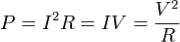
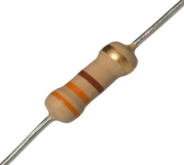
Fig 3.3.12: Resistor
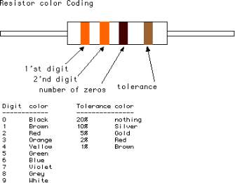
Fig 3.3.13: Color Bands In Resistor
3.4. LED
A light-emitting diode (LED) is a semiconductor light source. LED’s are used as indicator lamps in many devices, and are increasingly used for lighting. Introduced as a practical electronic component in 1962, early LED’s emitted low-intensity red light, but modern versions are available across the visible, ultraviolet and infrared wavelengths, with very high brightness. The internal structure and parts of a led are shown in figures 3.4.1 and 3.4.2 respectively.
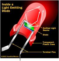
Fig 3.4.1: Inside a LED
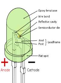
Fig 3.4.2: Parts of a LED
Working:
The structure of the LED light is completely different than that of the light bulb. Amazingly, the LED has a simple and strong structure. The light-emitting semiconductor material is what determines the LED’s color. The LED is based on the semiconductor diode.
When a diode is forward biased (switched on), electrons are able to recombine with holes within the device, releasing energy in the form of photons. This effect is called electroluminescence and the color of the light (corresponding to the energy of the photon) is determined by the energy gap of the semiconductor. An LED is usually small in area (less than 1 mm2), and integrated optical components are used to shape its radiation pattern and assist in reflection. LED’s present many advantages over incandescent light sources including lower energy consumption, longer lifetime, improved robustness, smaller size, faster switching, and greater durability and reliability. However, they are relatively expensive and require more precise current and heat management than traditional light sources. Current LED products for general lighting are more expensive to buy than fluorescent lamp sources of comparable output. They also enjoy use in applications as diverse as replacements for traditional light sources in automotive lighting (particularly indicators) and in traffic signals. The compact size of LED’s has allowed new text and video displays and sensors to be developed, while their high switching rates are useful in advanced communications technology. The electrical symbol and polarities of led are shown in fig: 3.4.3.
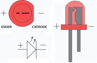
Fig 3.4.3: Electrical Symbol & Polarities of LED
LED lights have a variety of advantages over other light sources:
- High-levels of brightness and intensity
- High-efficiency
- Low-voltage and current requirements
- Low radiated heat
- High reliability (resistant to shock and vibration)
- No UV Rays
- Long source life
- Can be easily controlled and programmed
Applications of LED fall into three major categories:
- Visual signal application where the light goes more or less directly from the LED to the human eye, to convey a message or meaning.
- Illumination where LED light is reflected from object to give visual response of these objects.
- Generate light for measuring and interacting with processes that do not involve the human visual system.
3.5 Personal computer
PC is the main element of the communication between the PC and the Micro Controller, PC sends the data to be transmitted to the receiver side device, but the data cannot be transmitted directly from the computer, so it employs a serial communication with the Micro Controller. This requires a Micro Controller to be connected to the PC, so that it is programmed in order to receive data from the computer and transmit the data to the receiver section through the transmitting antenna.
3.6 LCD DISPLAY
LCD Background:
One of the most common devices attached to a micro controller is an LCD display. Some of the most common LCD’s connected to the many microcontrollers are 16×2 and 20×2 displays. This means 16 characters per line by 2 lines and 20 characters per line by 2 lines, respectively.
Basic 16x 2 Characters LCD
Figure 3.6.1: LCD Pin diagram
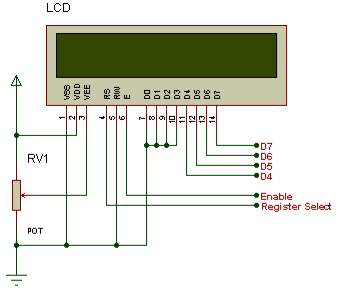
Pin description:
| Pin No. | Name | Description |
| Pin no. 1 | VSS | Power supply (GND) |
| Pin no. 2 | VCC | Power supply (+5V) |
| Pin no. 3 | VEE | Contrast adjust |
| Pin no. 4 | RS | 0 = Instruction input 1 = Data input |
| Pin no. 5 | R/W | 0 = Write to LCD module 1 = Read from LCD module |
| Pin no. 6 | EN | Enable signal |
| Pin no. 7 | D0 | Data bus line 0 (LSB) |
| Pin no. 8 | D1 | Data bus line 1 |
| Pin no. 9 | D2 | Data bus line 2 |
| Pin no. 10 | D3 | Data bus line 3 |
| Pin no. 11 | D4 | Data bus line 4 |
| Pin no. 12 | D5 | Data bus line 5 |
| Pin no. 13 | D6 | Data bus line 6 |
| Pin no. 14 | D7 | Data bus line 7 (MSB) |
Table 3.6.2: Character LCD pins with Microcontroller
The LCD requires 3 control lines as well as either 4 or 8 I/O lines for the data bus. The user may select whether the LCD is to operate with a 4-bit data bus or an 8-bit data bus. If a 4-bit data bus is used the LCD will require a total of 7 data lines (3 control lines plus the 4 lines for the data bus). If an 8-bit data bus is used the LCD will require a total of 11 data lines (3 control lines plus the 8 lines for the data bus). The three control lines are referred to as EN, RS, and RW.
The EN line is called “Enable.” This control line is used to tell the LCD that we are sending it data. To send data to the LCD, our program should make sure this line is low (0) and then set the other two control lines and/or put data on the data bus. When the other lines are completely ready, bring EN high (1) and wait for the minimum amount of time required by the LCD datasheet (this varies from LCD to LCD), and end by bringing it low (0) again.
The RS line is the “Register Select” line. When RS is low (0), the data is to be treated as a command or special instruction (such as clear screen, position cursor, etc.). When RS is high (1), the data being sent is text data which should be displayed on the screen. For example, to display the letter “T” on the screen we would set RS high.
The RW line is the “Read/Write” control line. When RW is low (0), the information on the data bus is being written to the LCD. When RW is high (1), the program is effectively querying (or reading) the LCD. Only one instruction (“Get LCD status”) is a read command. All others are write commands–so RW will almost always be low. Finally, the data bus consists of 4 or 8 lines (depending on the mode of operation selected by the user). In the case of an 8-bit data bus, the lines are referred to as DB0, DB1, DB2, DB3, DB4, DB5, DB6, and DB7.
Schematic:
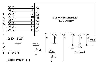
Figure 3.6.3: LCDSchematic Pin diagram
Circuit Description:
Above is the quite simple schematic. The LCD panel’s Enable and RegisterSelect is connected to the Control Port. The Control Port is an open collector / open drain output. While most Parallel Ports have internal pull-up resistors, there is a few which don’t. Therefore by incorporating the two 10K external pull up resistors, the circuit is more portable for a wider range of computers, some of which may have no internal pull up resistors.
We make no effort to place the Data bus into reverse direction. Therefore we hard wire the R/W line of the LCD panel, into write mode. This will cause no bus conflicts on the data lines. As a result we cannot read back the LCD’s internal Busy Flag which tells us if the LCD has accepted and finished processing the last instruction. This problem is overcome by inserting known delays into our program.
The 10k Potentiometer controls the contrast of the LCD panel. Nothing fancy here. As with all the examples, I’ve left the power supply out. We can use a bench power supply set to 5v or use an onboard +5 regulator. Remember a few de-coupling capacitors, especially if we have trouble with the circuit working properly.
SETB RW
Handling the EN control line:
As we mentioned above, the EN line is used to tell the LCD that we are ready for it to execute an instruction that we’ve prepared on the data bus and on the other control lines. Note that the EN line must be raised/ lowered before/after each instruction sent to the LCD regardless of whether that instruction is read or write text or instruction. In short, we must always manipulate EN when communicating with the LCD. EN is the LCD’s way of knowing that we are talking to it. If we don’t raise/lower EN, the LCD doesn’t know we’re talking to it on the other lines.
Thus, before we interact in any way with the LCD we will always bring the EN line low with the following instruction:
CLR EN
And once we’ve finished setting up our instruction with the other control lines and data bus lines, we’ll always bring this line high:
SETB EN
The line must be left high for the amount of time required by the LCD as specified in its datasheet. This is normally on the order of about 250 nanoseconds, but checks the datasheet. In the case of a typical microcontroller running at 12 MHz, an instruction requires 1.08 microseconds to execute so the EN line can be brought low the very next instruction. However, faster microcontrollers (such as the DS89C420 which executes an instruction in 90 nanoseconds given an 11.0592 MHz crystal) will require a number of NOPs to create a delay while EN is held
high. The number of NOPs that must be inserted depends on the microcontroller we are using and the crystal we have selected.
The instruction is executed by the LCD at the moment the EN line is brought low with a final CLR EN instruction.
Checking the busy status of the LCD:
As previously mentioned, it takes a certain amount of time for each instruction to be executed by the LCD. The delay varies depending on the frequency of the crystal attached to the oscillator input of the LCD as well as the instruction which is being executed.
While it is possible to write code that waits for a specific amount of time to allow the LCD to execute instructions, this method of “waiting” is not very flexible. If the crystal frequency is changed, the software will need to be modified. A more robust method of programming is to use the “Get LCD Status” command to determine whether the LCD is still busy executing the last instruction received.The “Get LCD Status” command will return to us two tidbits of information; the information that is useful to us right now is found in DB7. In summary, when we issue the “Get LCD Status” command the LCD will immediately raise DB7 if it’s still busy executing a command or lower DB7 to indicate that the LCD is no longer occupied. Thus our program can query the LCD until DB7 goes low, indicating the LCD is no longer busy. At that point we are free to continue and send the next command.
Applications:
- Medical equipment
- Electronic test equipment
- Industrial machinery Interface
- Serial terminal
- Advertising system
- EPOS
- Restaurant ordering systems
- Gaming box
- Security systems
- R&D Test units
- Climatizing units
- PLC Interface
- Simulators
- Environmental monitoring
- Lab development
- Student projects
- Home automation
- PC external display
- HMI operator interface.
3.7 BUZZER
A buzzer or beeper is an audio signaling device, which may be mechanical, electromechanical, or piezoelectric. Typical uses of buzzers and beepers include alarm devices, timers and confirmation of user input such as a mouse click or keystroke.
Mechanical
A joy buzzer is an example of a purely mechanical buzzer.
Fig 3.7.1 (a) : Mechanical joy buzzer
Electromechanical
Early devices were based on an electromechanical system identical to an electric bell without the metal going. Similarly, a relay may be connected to interrupt its own actuating current, causing the contacts to buzz. Often these units were anchored to a wall or ceiling to use it as a sounding board. The word “buzzer” comes from the rasping noise that electromechanical buzzers made.
Piezoelectric
Nowadays, it is more popular to use a ceramic-based piezoelectric sounder like a Son alert which makes a high-pitched tone. Usually these were hooked up to “driver” circuits, which varied the pitch of the sound or pulsed the sound on and off.
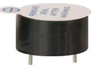
Fig(3.7.2): picture of buzzer
A piezoelectric element may be driven by an oscillating electronic circuit or other audio signal source, driven with a piezoelectric audio amplifier. Sounds commonly used to indicate that a button has been pressed are a click, a ring or a beep. Piezo buzzer is an electronic device commonly used to produce sound. Light weight, simple construction and low price make it usable in various applications like car/truck reversing indicator, computers, call bells etc.
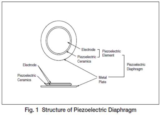
Basically, the sound source of a piezoelectric sound component is a piezoelectric diaphragm as shown in fig(3.7.3). A piezoelectric diaphragm consists of a piezoelectric ceramic plate which has electrodes on both sides and a metal plate (brass or stainless steel, etc.).
A piezoelectric ceramic plate is attached to a metal plate with adhesives. Applying D.C. voltage between electrodes of a piezoelectric diaphragm causes mechanical distortion due to the piezoelectric effect. For a misshaped piezoelectric element, the distortion of the piezoelectric element expands in a radial direction. And the piezoelectric diaphragm bends toward the direction. The metal plate bonded to the piezoelectric element does not expand.
Conversely, when the piezoelectric element shrinks, the piezoelectric diaphragm bends in the direction Thus, when AC voltage is applied across electrodes, the bending is repeated, producing sound waves in the air.
Buzzers typically provide a user with an alert when a given condition within the circuit has occurred. Normally man’s audible frequency range is 20Hz to 20kHz , but we can hear up to frequency ranges from 2kHz to 4kHz .
To interface a buzzer the standard transistor interfacing circuit is used(Fig 2). Note that if a different power supply is used for the buzzer, the 0V rails of each power supply must be connected to provide a common reference. If a battery is used as the power supply, it is worth remembering that piezo sounders draw much less current than buzzers. Buzzers also just have one ‘tone’, whereas a piezo sounder is able to create sounds of many different tones. Here transistor acts as a switch.
To switch on buzzer -high 1
To switch off buzzer -low 1

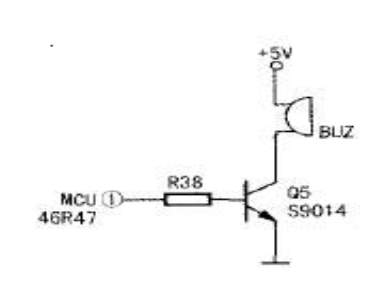
Fig.3.7.4 Buzzer with transistor interfacing circuit
Notice (Handling) In Using Self Drive Method:
1) When the piezoelectric buzzer is set to produce intermittent sounds, sound may be heard continuously even when the self drive circuit is turned ON / OFF at the “X” point shown in Fig(b). This is because of the failure of turning off the feedback voltage.
2) Build a circuit of the piezoelectric sounder exactly as per the recommended circuit shown in the catalog. Life of the transistor and circuit constants is designed to ensure stable oscillation of the piezoelectric sounder.
3) Design switching which ensures direct power switching.
4) The self drive circuit is already contained in the piezoelectric buzzer. So there is no need to prepare another circuit to drive the piezoelectric buzzer.
5) Rated voltage (3.0 to 20Vdc) must be maintained. Products which can operate with voltage higher than 20Vdc are also available.
6) Do not place resistors in series with the power source, as this may cause abnormal oscillation. If a resistor is essential to adjust sound pressure, place a capacitor (about 1μF) in parallel with the piezo buzzer.
7) Do not close the sound emitting hole on the front side of casing.
8) Carefully install the piezo buzzer so that no obstacle is placed within 15mm from the sound release hole on the front side of the casing.
3.8 ENCODERS & DECODERS SECTIONS
The Encoders are the devices which are used to encode the data where the Decoder is the device which is quite opposite to the Encoder. The Encoder used in the project are HT12E and Decoder is HT 12D.
HT 12E as RF encoder, HT 12D as RF decoder
The radio frequency spectrum is filled with noise and other signals, especially those frequencies where unlicensed transmitter operation under FCC part 15 rules is allowed. When using a wireless remote control system it is desirable to have a way of filtering out or ignoring those unwanted signals to prevent false data from being received.
A simple way to accomplish this is to use an encoder IC at the transmitter and a decoder IC at the receiver. The encoder generates serial codes that are automatically sent three times and must be received at least twice before data is accepted as valid by the decoder circuit and the information is being decoded using decoder circuitry.
HT12A/HT12E/212Series of Encoders
General Description:
The 2^12 encoders are a series of CMOS LSIs for remote control system applications. They are capable of encoding information which consists of N address bits and 12-N data bits. Each ad- dress/data input can be set to one of the two logic states. The programmed addresses/data are transmitted together with the header bits via an RF or an infrared transmission medium upon receipt of a trigger signal. The capability to select a TE trigger on the HT12E or a DATA trigger on the HT12A further enhances the application flexibility of the 212 series of encoders. The HT12A additionally provides a 38 kHz carrier for infrared systems.
- Minimum transmission word
- Four words for the HT12E
- One word for the HT12A
- Built-in oscillator needs only 5% resistor
- Data code has positive polarity
- Minimal external components
- HT12A/E: 18-pin DIP/20-pin SOP package
Features
- Operating voltage
- 2.4V~5V for the HT12A
- 2.4V~12V for the HT12E
- Low power and high noise immunity CMOS
- technology
- Low standby current: 0.1mA (type.) at
- VDD=5V
- HT12A with a 38kHz carrier for infrared
- transmission medium
Applications
- Burglar alarm system
- Smoke and fire alarm system
- Garage door controllers
- Car door controllers
- Car alarm system
- Security system
- Cordless telephones
- Other remote control systems
HT12D/HT12F/212 Series of Decoders:
The 212decoders are a series of CMOS LSI’s for remote control system applications. They are paired with Holtek’s 212series of encoders (refer to the encoder/de-coder cross reference table). For proper operation, a pair of encoder/decoder with the same number of ad-dresses and data format should be chosen. The decoders receive serial addresses and data from a programmed 212series of encoders that are transmitted by a carrier using an RF or an IR transmission medium. They compare the serial input data three times continuously with their local addresses. If no error or un-matched codes are found, the input data codes are decoded and then transferred to the output pins. The VT pin also goes high to indicate a valid transmission. The 212series of decoders are capable of decoding information that consist of N bits of address and 12-Nbits of data. Of this series, the HT12D is arranged to pro-vide 8 address bits and 4 data bits, and HT12F is used to decode 12 bits of address information.
Features
- Operating voltage: 2.4V~12V
- Low power and high noise immunity CMOS technology
- Low standby current
- Capable of decoding 12 bits of information
- Binary address setting
- Received codes are checked 3 times
- Address/Data number combination
- HT12D: 8 address bits and 4 data bits
- HT12F: 12 address bits only
- Built-in oscillator needs only 5% resistor
- Valid transmission indicator
- Easy interface with an RF or an infrared transmission medium
- Minimal external components
- Pair with Holtek’s 212series of encoders
- 18-pin DIP, 20-pin SOP package
Applications:
- Burglar alarm system
- Smoke and fire alarm system
- Garage door controllers
- Car door controllers
- Car alarm system
- Security system
- Cordless telephones
- Other remote control systems
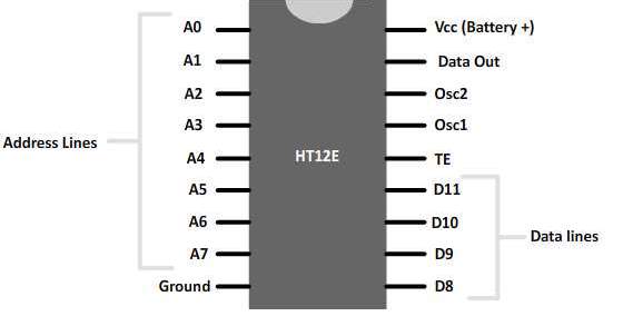
Fig: 3.8.1 Encoder
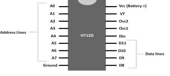
Fig: 3.8.2 Decoder
3.9 RS-232 Interface
The RS-232 interface is the Electronic Industries Association (EIA) standard for the interchange of serial binary data between two devices. It was initially developed by the EIA to standardize the connection of computers with telephone line modems. The standard allows as many as 20 signals to be defined, but gives complete freedom to the user. Three wires are sufficient: send data, receive data, and signal ground. The remaining lines can be hardwired on or off permanently. The signal transmission is bipolar, requiring two voltages, from 5 to 25 volts, of opposite polarity.
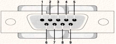
Fig 3.9.1. DB9 connector
3.9.1 Communication Standards
The industry custom is to use an asynchronous word consisting of: a start bit, seven or eight data bits, an optional parity bit and one or two stop bits. The baud rate at which the word sent is device-dependent. The baud rate is usually 150 times an integer power of 2, ranging from 0 to 7 (150, 300, 600, and 19,200). Below 150 baud, many system-unique rates are used. The standard RS-232-C connector has 25 pins, 21 pins which are used in the complete standard. Many of the modem signals are not needed when a computer terminal is connected directly to a computer.
The pin numbering used in the original DB-25 connector and that now commonly used with a DB-9 connector is normally used in modern computers. Specifying compliance to RS-232 only establishes that the signal levels in two devices will be compatible and that if both devices use the suggested connector, they may be able to be connected. Compliance to RS-232 does not imply that the devices will be able to communicate or even acknowledge each other’s presence.
Fig 3.9.2 Direct-to-computer rs-232 interface
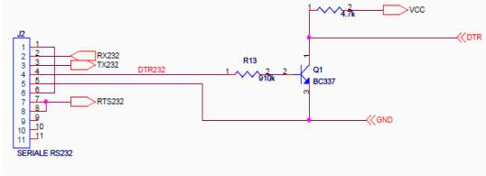
Fig :3.9.3 schematic of RS-232 Interface
Fig: 3.9.4Table RS-232 DB9 Pins
| Pin | Description |
|
|
Data carrier detect (DCD) |
|
|
Received data (RXD) |
|
|
Transmitted data (TXD) |
|
|
Data Terminal Ready (DTR) |
|
|
Ground(GND) |
|
|
Data Set Ready (DSR) |
| 7 | Request To Send (RTS) |
| 8 | Clear To Send (CTS) |
| 9 | Ring Indicator (RI) |
RS – 232 Interface
Port RS232 is signal RS232 level that has already transformed to be signal Level of MAX232, so it can be connected with signal RS232 to send/receive data. Additionally, it can be used with Switch LOAD and Switch RESET to Download Hex File into CPU.
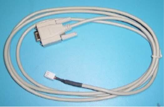
Fig 3.9.5 RS-232 cable
MAX232
MAX232 is compatible with RS-232 standard, and consists of dual transceiver. Each receiver converts TIA/EIA-232-E levels into 5V TTL/CMOS levels. Each driver converts TTL/COMS levels into TIA/EIA-232-E levels. The MAX232 is characterized for operation from -40°C to +85°C for all packages. MAX232 is purposed for application in high-performance information processing systems and control devices of wide application.The max 232 are a dual driver/receiver that includes a capacitive voltage generator to supply TIA/EIA-232F voltage levels from a single 5v supply. Each receiver converts TIA/EIA-232F inputs to 5vTTL/CMOS levels. These receivers have a typical threshold of 1.3V, a typical hysteresis of 0.5V, and can accept ±30V inputs. Each driver converts TTL/CMOS input level into TIA/EIA-232F levels.
Recommended operating conditions
| Min Nom Max | UNIT | |
| Vcc Supply voltage | 4.5 5 5.5 | V |
| VIH High-Level input voltage(T1IN,T2IN) | 2 | V |
| VIL Low-Level input voltage(T1IN,T2IN) | 0.8 | V |
| R1IN,R2IN Receiver input voltage | ±30 | V |
Fig 3.9.6 Table recommended operating conditions
Functions tables
Each Driver
| INPUT Tin | OUTPUT Tout |
| L | H |
| H | L |
Each receiver
| INPUT Tin | OUTPUT Tout |
| L | H |
| H | L |
H= high level, L = low level
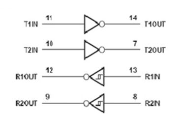
Fig: 3.9.7 Function Tables
Fig 3.9.8 logic diagram of MAX232
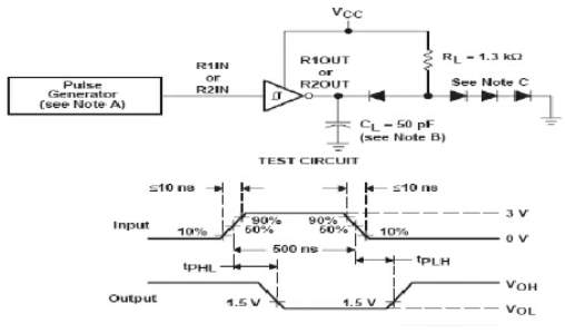
Fig 3.9.9 Parameter measurement information
The pulse generator has the following characteristics: ZO = 50 Ω, duty cycle ≤ 50%.B. All diodes are 1N3064 or equivalent.
Fig 3.9.10 receiver test circuit and waveforms for tPHL and tPLH measurements
Schematic of max-232
The MAX232 is a dual driver/receiver that includes a capacitive voltage generator to supply EIA-232 voltage levels from a single 5-V supply. Each receiver converts EIA-232 inputs to 5-V TTL/CMOS levels. The schematic of MAX 232 is shown in Fig
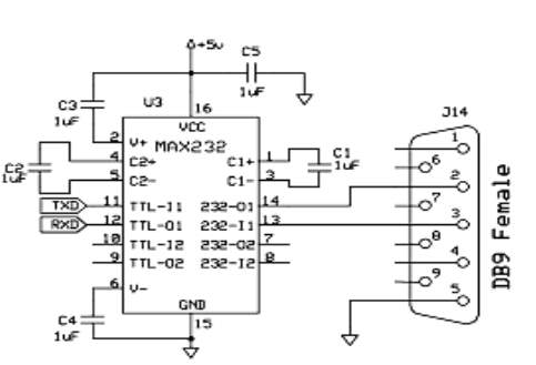
Fig 3.9.11 Schematic diagram of MAX-232
These receivers have a typical threshold of 1.3 V and a typical hysteresis of 0.5 V, and can accept ±30-V inputs. Each driver converts TTL/CMOS input levels into EIA-232 levels.
RF SECTION
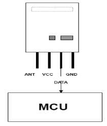
This section is basically used to transmit and receive the data wirelessly. The devices used to do the same are RF Transmitter and RF Receiver.
3.10 RF TRANSMITTER
RF transmitters are electronic devices that create continuously varying electric current, encode sine waves, and broadcast radio waves. RF transmitters use oscillators to create sine waves, the simplest and smoothest form of continuously varying waves, which contain information such as audio and video. Modulators encode these sign wives and antennas broadcast them as radio signals. There are several ways to encode or modulate this information, including amplitude modulation (AM) and frequency modulation (FM). Radio techniques limit localized interference and noise. With direct sequence spread spectrum, signals are spread over a large band by multiplexing the signal with a code or signature that modulates each bit. With frequency hopping spread spectrum, signals move through a narrow set of channels in a sequential, cyclical, and predetermined pattern.
Selecting RF transmitters requires an understanding of modulation methods such as AM and FM. On-off key (OOK), the simplest form of modulation, consists of turning the signal on or off. Amplitude modulation (AM) causes the baseband signal to vary the amplitude or height of the carrier wave to create the desired information content. Frequency modulation (FM) causes the instantaneous frequency of a sine wave carrier to depart from the center frequency by an amount proportional to the instantaneous value of the modulating signal. Amplitude shift key (ASK) transmits data by varying the amplitude of the transmitted signal. Frequency shift key (FSK) is a digital modulation scheme using two or more output frequencies. Phase shift key (PSK) is a digital modulation scheme in which the phase of the transmitted signal is varied in accordance with the base band data signal.
Additional considerations when selecting RF transmitters include supply voltage, supply current, RF connectors, special features, and packaging. Some RF transmitters include visual or audible alarms or LED indicators that signal operating modes such as power on or reception. Other devices attach to coaxial cables or include a connector or port to which an antenna can be attached. Typically, RF transmitters that are rated for outdoor use feature a heavy-duty waterproof design. Devices with internal calibration and a frequency range switch are also available.
RF transmitters are used in a variety of applications and industries. Often, devices that are used with integrated circuits (ICs) incorporate surface mount technology (SMT), Through Hole Technology (THT), and flat pack. In the telecommunications industry, RF transmitters are designed to fit in a metal rack that can be installed in a cabinet. RF transmitters are also used in radios and in electronic article surveillance systems (EAS) found in retail stores. Inventory management systems use RF transmitters as an alternative to barcodes.
ASK Transmitter Module (ST-TX01-ASK (Saw Type)
General Description:
The ST-TX01-ASK is an ASK Hybrid transmitter module. ST-TX01-ASK are designed by the Saw Resonator, with an effective low cost, small size, and simple-to-use for designing.
Frequency Range: 315 / 433.92 MHZ.
Supply Voltage: 3~12V.
Output Power: 4~16dBm.
Circuit Shape: Saw.
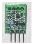
Fig:3.10.1 315/434 MHz ASK TRANSMITTER
Applications
- Wireless security systems
- Car Alarm systems
- Remote controls.
- Sensor reporting
- Automation systems
Here in this project the RF transmitter module is not directly connected to microcontroller. An Encoder is connected between the RF module and the controller, in order to encode the data for efficient transmission of the data
3.11 RF RECEIVER
RF receivers are electronic devices that separate radio signals from one another and convert specific signals into audio, video, or data formats. RF receivers use an antenna to receive transmitted radio signals and a tuner to separate a specific signal from all of the other signals that the antenna receives. Detectors or demodulators then extract information that was encoded before transmission. There are several ways to decode or demodulate this information, including amplitude modulation (AM) and frequency modulation (FM). Radio techniques limit localized interference and noise. With direct sequence spread spectrum, signals are spread over a large band by multiplexing the signal with a code or signature that modulates each bit. With frequency hopping spread spectrum, signals move through a narrow set of channels in a sequential, cyclical, and predetermined pattern.
Selecting RF receivers requires an understanding of modulation methods such as AM and FM. On-off key (OOK), the simplest form of modulation, consists of turning the signal on or off. Amplitude modulation (AM) causes the base band signal to vary the amplitude or height of the carrier wave to create the desired information content. Frequency modulation (FM) causes the instantaneous frequency of a sine wave carrier to depart from the center frequency by an amount proportional to the instantaneous value of the modulating signal. Amplitude shift key (ASK) transmits data by varying the amplitude of the transmitted signal. Frequency shift key (FSK) is a digital modulation scheme using two or more output frequencies. Phase shift key (PSK) is a digital modulation scheme in which the phase of the transmitted signal is varied in accordance with the base band data signal.
RF receivers vary in terms of performance specifications such as sensitivity, digital sampling rate, measurement resolution, operating frequency, and communication interface. Sensitivity is the minimum input signal required to produce a specified output signal having a specified signal-to-noise (S/N) ratio. Digital sampling rate is the rate at which samples can be drawn from a digital signal in kilo samples per second. Measurement resolution is the minimum digital resolution, while operating frequency is the range of received signals. Communication interface is the method used to output data to computers. Parallel interfaces include general-purpose interface bus (GPIB), which is also known as IEEE 488 and HPIB Protocol. Serial interfaces include universal serial bus (USB), RS232, and RS485.
Additional considerations when selecting RF receivers include supply voltage, supply current, receiver inputs, RF connectors, special features, and packaging. Some RF receivers include visual or audible alarms or LED indicators that signal operating modes such as power on or reception. Other devices attach to coaxial cables or include a connector or port to which an antenna can be attached. Typically, RF receivers that are rated for outdoor use feature a heavy-duty waterproof design. Devices with internal calibration and a frequency range switch are also available.
Description:
The RX04 is a low-power ASK Receiver IC which is fully compatible with the Mitel KESRX01 IC and is suitable for use in a variety of low power radio applications including remote keyless entry. The RX04 is based on a single-conversion, super-heterodyne receiver architecture and incorporates an entire phase-locked loop (PLL) for precise local oscillator generation.
Applications:
- Car security system
- Wireless security systems
- Sensor reporting
- automation system
- Remote Keyless entry
Features
- Low power consumption.
- Easy for application.
- On-Chip VCO with integrated PLL using crystal oscillator reference.
- Integrated IF and data filters.
- Operation temperature range : ﹣10℃~+60℃
- Operation voltage: 5 Volts.
- Available frequency at : 315/434 MHz
Functional description:
Fig: 3.11.1 315/434 MHz ASK RECEIVER
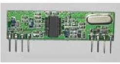
PIN DIAGRAM
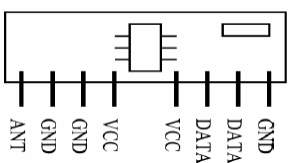
Fig 3.11.2 RF receiver module
In this RF receiver is connected as shown in the schematic. The DATA pin is connected to the decoder HT648L which decodes the received signal and gives to the microcontroller.
CHAPTER 4: SOFTWARE DESCRIPTION
4.1 EXPRESS PCB
Breadboards are great for prototyping equipment as it allows great flexibility to modify a design when needed; however the final product of a project, ideally should have a neat PCB, few cables, and survive a shake test. Not only is a proper PCB neater but it is also more durable as there are no cables which can yank loose.
Express PCB is a software tool to design PCBs specifically for manufacture by the company Express PCB (no other PCB maker accepts Express PCB files). It is very easy to use, but it does have several limitations.
It can be likened to more of a toy then a professional CAD program.
It has a poor part library (which we can work around).
It cannot import or export files in different formats.
It cannot be used to make prepare boards for DIY production.
Express PCB has been used to design many PCBs (some layered and with surface-mount parts. Print out PCB patterns and use the toner transfer method with an Etch Resistant Pen to make boards. However, Express PCB does not have a nice print layout. Here is the procedure to design in Express PCB and clean up the patterns so they print nicely.
4.2 Keil software
- Click on the Keil u Vision Icon on Desktop
- The following fig will appear
- Click on the Project menu from the title bar
- Then Click on New Project
- Save the Project by typing suitable project name with no extension in u r own folder sited in either C: or D:

- Then Click on Save button above.
- Select the component for u r project. i.e. Atmel……
- Click on the + Symbol beside of Atmel
- Select AT89C51 as shown below
- Then Click on “OK”
- The Following fig will appear
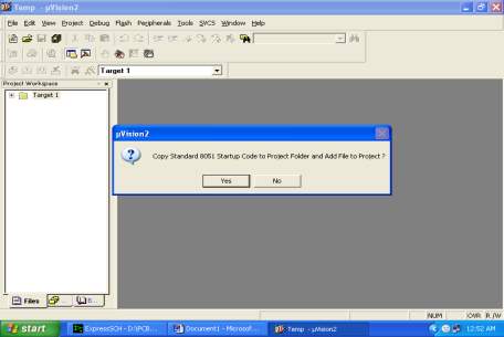
- Then Click either YES or NO………mostly “NO”
- Now your project is ready to USE
- Now double click on the Target1, you would get another option “Source group 1” as shown in next page.
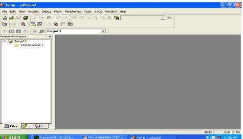
- Click on the file option from menu bar and select “new”
- The next screen will be as shown in next page, and just maximize it by double clicking on its blue boarder.
- Now start writing program in either in “C” or “ASM”
- For a program written in Assembly, then save it with extension “. asm” and for “C” based program save it with extension “ .C”
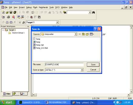
- Now right click on Source group 1 and click on “Add files to Group Source”
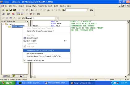
- Now you will get another window, on which by default “C” files will appear.
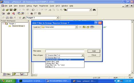
- Now select as per your file extension given while saving the file
- Click only one time on option “ADD”
- Now Press function key F7 to compile. Any error will appear if so happen.
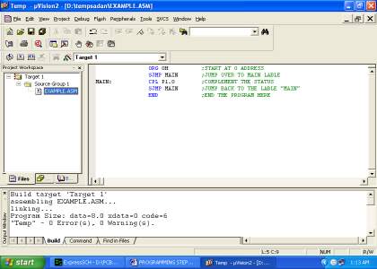
- If the file contains no error, then press Control+F5 simultaneously.
- The new window is as follows
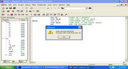
- Then Click “OK”
- Now Click on the Peripherals from menu bar, and check your required port as shown in fig below
- Drag the port a side and click in the program file.
- Now keep Pressing function key “F11” slowly and observe.
- You are running your program successfully
4.3 Flash magic
Flash Magic is an application developed by Embedded Systems Academy to allow you to easily access the features of a microcontroller device. With this program you can erase individual blocks or the entire Flash memory of the microcontroller.
This application is very useful for those who work in the electronics field. The main window of the program is composed of five sections where you can find the most common functions in order to program a microcontroller device. Using the “Communications” section you will be able to choose the way a specific device connects to your computer. Select the COM port to be used and the baud rate. It is recommended that you choose a low baud rate first and increase it afterwards. This way you will determine the highest speed with which your system works. In order to select which parts of the memory to erase, choose from the items in the “Erase” section. The third section is optional. It offers you the possibility to program a HEX file. In the next section you will be able to find different programming options, such as “verify after programming”, “gen block checksums”, “execute” and others. When you’re done, click the Start button that can be found in the “Start” section. The program will start the device, and you will able to see the progress of the operations at the bottom of the main window.
Using Flash Magic, you are able to perform different operations to a microcontroller device, operations like erasing, programming and reading the flash memory, modifying the Boot Vector, performing a blank check on a section of the Flash memory and many others.
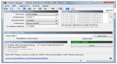
Fig: 4.3.1 Flash magic main window
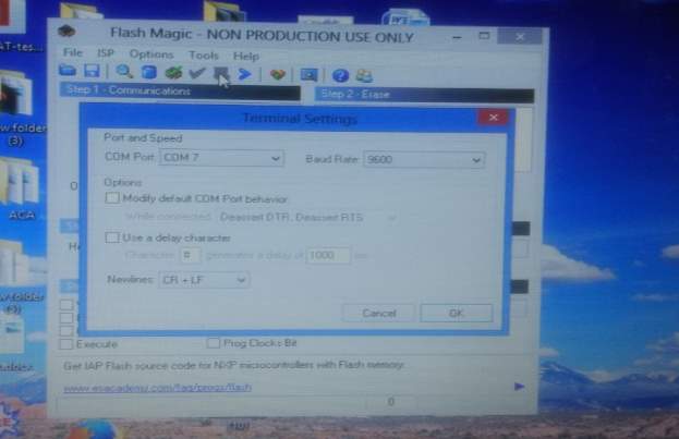
Fig 4.3.2 (terminal)
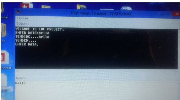
Fig 4.3.3 (text window)
CHAPTER 5: PROJECT DESCRIPTION
In this chapter, schematic diagram and interfacing of AT89S52 microcontroller with each module is considered
5.1 Working
There is a detailed description in this project about secured wireless communication. This means that our data which is to be sent through wireless medium should be safe. At the transmitter there is attached a keyboard which is used to input our message. This message will be encrypted and then transmitted through RF transmitter. These characters which are to be transmitted will also be displayed on the PC which is attached to microcontroller. At the receiver end when the encrypted message is received then this message is decrypted by the microcontroller and is displayed on the LCD. The mode of communication that we have used in our project is radio frequency.
The data is transmitted serially from pc to the controller is done using max232 cables. The encoder, encodes the data and is transmitted by using a RF transmitted from the transmitter circuit. The transmitted data is caught hold at the receiver circuit and is receiver circuit and is decoded by using the decoder and the decode data Can be seen in the LCD.
The circuit works on the +5v RPS. We will use TX and RX, for transmission and reception of the RF signals. The software part is programmed in keil software depending upon the program the microcontroller works.
The AT89S52 micro controller has reusable flash memories which are an added advantage. The operating frequency of transmitter and receiver of RF module is about 433mhz.
Transmitter section
The input is given to the system using computer keyboard. This input is fed into the AT89S52 microcontroller. In this microcontroller the message which being entered is encrypted according to a specific algorithm. After this it is encoded using RF encoder and finally this encoded signal is sent to the RF transmitter which transmits that message.
Fig : 5.1.1 Schematic diagram of Transmitter section
Receiver section
In the receiver section RF receiver receives the encrypted message and then sends this message to the RF decoder. After decoding that signals the RF decoder then send this signal to the microcontroller which decrypts that message and finally that message is displayed on the LCD.
Fig : 5.1.2 Schematic diagram of receiver section
Program :
Transmitter section Program:
/*************** PC-PC COMMUNICATION WITH CRYPTOGRAPHY UISNG 4-BIT RF***********
MODULES :
Transmitter section:
PC (P3.0,P3.1)
AT89S52
RF TX 4-bit DATA (P1.0-P1.3) TE -P3.2
Receiver section:
AT89S52
RF RX 4-bit DATA (P1.0-P1.3) VT -P3.2
PC (P3.0,P3.1)
**********************************************************/
/***************** HEADDER FILES ********************/
#include
#include
/*********** PIN CONNECTIONS ************/
sfr rfdata =0x90;
sbit te=P3^2;
/************* VARIABLE DECLARATIONS ************/
unsigned char a[30],i,k,t;
bit f1;
/*************** SERIAL ISR **********/
void serialint (void) interrupt 4
{
if (RI)
{
t=SBUF;
a[i]=t;
if(a[i]==0x0d){f1=1;a[i]=’�′;}
else{EA=0;serial_tx(a[i]);EA=1;}
i++;
RI=0;delay1(10);
}
}
/******************* RF TRANS fun***************/
void trans_tx(unsigned char t)
{
unsigned char t1,t2;
serial_tx(t);
t1=t & 0x0f;t1=t1|0xf0;
t2=t & 0xf0;t2=t2>>4;t2=t2|0xf0;
rfdata=t2;
te=0;
delay1(20);
te=1;
delay1(30);
rfdata=t1;
te=0;
delay1(20);
te=1;
}
void trans(unsigned char *x)
{
while(*x!=’�′)
{
trans_tx(*x++);
delay1(50);
}
}
/*************** MAIN FUNCTION ****************/
void main()
{
te=1;
/************ SERIAL INITILISATIONS *******/
sconfig();
serial_tx(0x0d);
serial_tx(0x0a);
serial(“WELCOME TO THE PROJECT:”);
serial_tx(0x0d);
serial_tx(0x0a);
serial(“ENTER DATA:”);
EA=1;
ES=1;
f1=0;i=0;
while(1)
{
if(f1==1)
{
EA=0;
serial_tx(0x0a);
serial(“SENDING….”);
delay1(250);
trans(a);
trans_tx(0x0d);
serial(“SENDED….”);
serial_tx(0x0d);
serial_tx(0x0a);
serial(“ENTER DATA:”);
EA=1;f1=0;i=0;
}
}
}
Receiver section Program:
/****** PC-PC COMMUNICATION WITH CRYPTOGRAPHY UISNG 4-BIT RF*******
MODULES :
Transmitter section:
PC (P3.0,P3.1)
AT89S51
RF TX 4-bit DATA (P1.0-P1.3) TE -P3.2
Reciver section:
AT89S1
PC (P3.0,P3.1)
RF RX 8-bit DATA (P1.0-P1.3) VT -P3.2
**********************************************************/
/***************** HEADDER FILES ********************/
#include
#include
#include
/*********** PIN CONNECTIONS ************/
sfr rfdata =0x90;
sbit vt=P3^2;
/************* VARIABLE DECLARATIONS ************/
static unsigned char a[60],c[30];
unsigned char t,k,i;
bit f1,f2;
/*************** EXTERNAL ISR **********/
void externalint (void) interrupt 0 using 1
{
t=rfdata&0x0f;
t=t|0xf0;
a[i]=t;
if((a[i-1]==0xf0)&& (a[i]==0xfd))
{f2=1;a[i-1]=’�′;}
i++;
}
void receive (unsigned char *s)
{
unsigned char t1,t2;k=0;
while(*s!=’�′)
{
t2=*s++;
t2=t2 & 0x0f;t2=t2
t1=*s++;
t1=t1&0x0f;
c[k]=t1|t2;
lcd_disp(c[k++]);
}
c[k]=’�′;
}
/*************** MAIN FUNCTION ****************/
void main()
{
rfdata=0xff;vt=1;
/************** SERIAL INITILISATIONS ***/
EA=1;
EX0=1;IT0=1;i=0;
f1=0;f2=0;ES=1;
while(1)
{lcd_cmd(0X80);
lcd_disp(“WELCOME TO “);
lcd_cmd(0XC0);
lcd_disp(“THE PROJECT”);
if(f2==1)
{
EA=0;EX0=0;
receive(a);
}
}
}
CHAPTER 6: ADVANTAGES, DISADVANTAGES, APPLICATIONS
6.1 ADVANTAGES
- Security.
- No line of sight is required.
- Speed of transmission.
- Not as sensitive to weather/environmental conditions .
- Easy to implement.
- Unlimited data transfer
6.2 DISADVANTAGES
- Since it is a wireless communication sometimes the atmosphere may disturb the Signals this results data loss.
- wireless Phones, scanners, wrist radios and personal locators can interfere with Transmission.
- We have to use separate radio band, which may be expensive.
6.3 APPLICATIONS
- Military application
- Government’s secure data transmission
- Storage devices ( USB )
- Wireless devices
- ATMs
CHAPTER 7: RESULTS
7.1 RESULTS
This project was designed to protect the data from hackers wirelessly using RF. This project is implemented 8051 based At89s52 developed board interfaced with RF Tx, RF Rx, Encoder, Decoder, keypad and LCD for displaying the data. Wireless communication is very important in many fields where secure data communication is required.
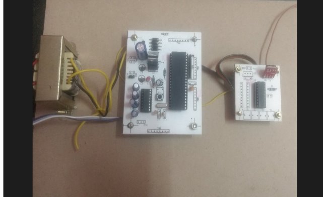
Fig 7.1.1 Screenshot of Transmitter Section of Wireless Secured Data Transmisssion using RF
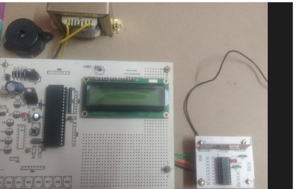
Fig 7.1.2 Screenshot of Receiver Section of Wireless Secured Data Transmission using RF
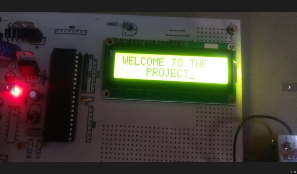
Fig7.1.3 Screenshot of Receiver Section when “ON” condition of Wireless Secured Data Transmission using RF
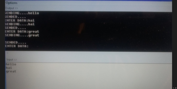
Fig 7.1.4 Screenshot of input given by the transmitter to receiver with PC
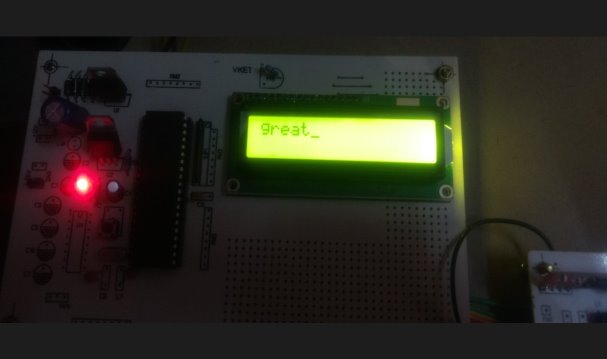
Fig 7.1.5 Screenshot of output displayed at receiver on LCD
CHAPTER 8: CONCLUSION, FUTURE PROSPECTS
8.1 CONCLUSION
Through this technique we can send any type of data with high level of security, by making the modifications in input and output devices. This is embedded based so we can make our own algorithm in micro controller for more security concern. We can use these high level security transfer systems for banking , military and online shopping . We can use the powerful antennas for longer communication.
8.2 FUTURE PROSPECTS
This project can be modified in many ways. Some of the additional features that can be added to this project are:
- The project that we have designed is based on simplex communication. It can be enhanced to a duplex mode of communication.
- A proper key management scheme for the encryption and decryption processes can also be implemented on this project to ensure more data security
- This project can also be implemented using long range RF modules
- This device is only a secure text terminal capable of transmitting alphabets and characters.
- Instead of present one to one communication protocol the device can be enhanced for working with other devices in a local area network.
- This project should be upgraded and enhanced to allow transmission and reception even under jammer on conditions.
REFERENCES
The sites which were used while doing this project:
Books referred
- Raj kamal –Microcontrollers Architecture, Programming, Interfacing and System Design.
- Mazidi and Mazidi –Embedded Systems.
- PCB Design Tutorial –David.L.Jones.
- Embedded C –Michael.J.Pont.
Cite This Work
To export a reference to this article please select a referencing stye below:
Related Services
View all


Related Content
All TagsContent relating to: "Technology"
Technology can be described as the use of scientific and advanced knowledge to meet the requirements of humans. Technology is continuously developing, and is used in almost all aspects of life.
Related Articles

DMCA / Removal Request
If you are the original writer of this dissertation and no longer wish to have your work published on the UKDiss.com website then please: