Single Phase Multi-channel Inverter
Info: 9078 words (36 pages) Dissertation
Published: 16th Dec 2019
Tagged: ElectronicsEnergy
CHAPTER-1
INTRODUCTION
The conventional energy supplied by the electricity department is not able to meet the demand, & because of the power deficiency people are accepting power cuts. Particularly at domestic side many groups of people are facing many problems because of frequent power cuts, to avoid this problem alternative power source is essential. In this regard power inverters are essential to overcome this problem and hence this project work is taken up. The main concept involved in the system is to provide stand-by power in emergencies. In general for most applications, single power source is used as stand-by power. This concept is aimed to provide supply to the load during the absence of main power. But in many cases, we find that power systems often fails due to many reasons, for emergency services like hospitals additional stand-by power source essential and there by this multi-channel power source concept is presented in this project work. The same system can be used for domestic applications to drive domestic loads like ceiling fan, TV, tube light, etc. Since it is a prototype module, low power inverter is designed so that each channel can deliver a maximum power output of 80W. The charging circuit is designed to charge any one battery and desired battery can be selected through mode switch. If required solar panels can be used to charge the batteries.
Since it is a prototype module, the battery used here is not sufficient run the appliances continuously, to run the devices continuously huge rating batteries are essential. The power system designed here can be utilized to drive a maximum load of 80Watts. The prototype module contains all required devices including 7.5AH battery, which makes the system as real working. The first & important application is to run a ceiling fan, for this purpose single phase supply is generated from 12V battery, latest technology is implemented such that if required fan speed can be varied linearly by switching the power
MOSFETS through PWM chip. Here high efficiency inverter is designed to minimize the energy losses.
The power system is designed to deliver 220V ac from 12V DC source availed from the battery. For this purpose high power rechargeable battery is used a back-up source, there by the system can be used to drive the load when required. As this power system can be modified according to the requirements, and by using solar energy to charge the battery, it is quite useful for remote areas, where the availability of main power is critical.
We are using solar energy for charging battery, it is essential to describe about utilization of solar energy, because these days lot of importance is given for solar energy. Solar energy is increasingly used these days for wide variety of applications. As the availability of fossil fuel declines, there is need to find alternate energy sources, of the many sources, solar energy available in abundance and renewable is the ultimate source of all known forms of energy. It is clear, safe, and free, does not pollute the environment and thus will be an extremely viable alternative in the days to come.
One way to utilize the solar energy is to generate electricity directly from the sunlight by photovoltaic conversion. Since photovoltaic modules have now become extensively available in the country. Solar energy has long been regarded as an ideal energy source but for the fact that we knew little to tap or use it to our advantage. The advancement in science and technology brought out by mankind had lead to developments like the photovoltaic cell. Solar panels comprise of a number of such P V Cells. The output of the Solar Panel is proportional to the intensity of incident radiation from the sun.
As the power generated is dependent on incident radiation and also the intensity varies with time and season at a particular point, the efficiency of the fixed system is far less to exploit commercially. For optimum generation of electric power the PV Panels need to be maintained or positioned normal always to the incident radiation. This technique, known as Solar tracking, is therefore essential for improved system performance and efficiency. The resulting increase in efficiency is significant enough to make the tracking a viable proportion in-spite of the enhancement in the system cost. As this system is designed as prototype module, here panel is set to a fixed angle and it will not move according to the Sun direction. The panel used in the project work can deliver a maximum power of 10 watts under the bright Sun.
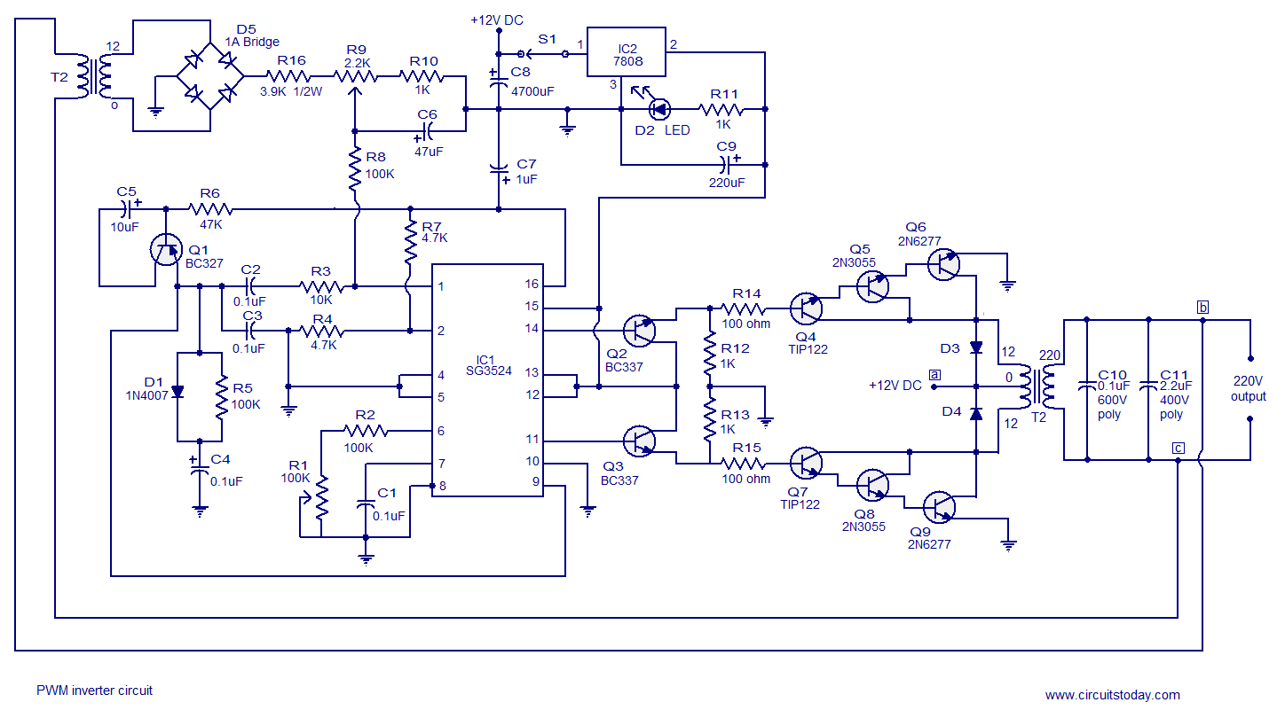
Now coming to the project work, In order to generate 230V ac from 12V battery for the inverter application, the best method of inverter with higher efficiency technique is to be evolved which shall be high efficient, less power consumption, easy interface, and modular design. For this purpose an IC 3524 based (pulse width modulator) circuit is designed which can work on a 12V sealed maintenance free battery there by it can provide an uninterruptible power supply. The main function of this power system is to provide power to the low power home appliances like fan, TV, light, etc., because the power system designed here can generate less power.
Initially the ac pulses at 50Hz in the form of square waves are generated from the inverter chip; this device generates duel inverted outputs. The output of the oscillator is amplified in terms of voltage and current, the drive circuit is designed with power mosfets & main output transformer, & it is configured as push-pull amplifier. With the help of a duty cycle control circuit interfaced with 3524 chip, output voltage is can be controlled linearly.
CHAPTER-2
BLOCK DIAGRAM
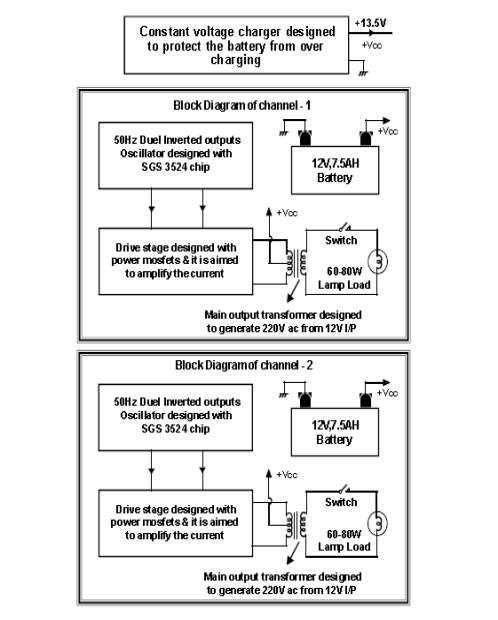
Fig 2.1-Block diagram
2.1 DESCRIPTION
The block diagram and its description of the project work “Single phase multi-channel inverter” is explained as per the individual blocks. The complete block diagram of the project work is shown above. The functional description of each block as per the main block diagram is explained in this chapter, in this regard the process starts from the battery. The required electrical energy to charge the battery is derived from main source, for this purpose step down transformer is used, rectified & filtered and is stored in the battery. With help of a regulator chip, constant voltage source is generated to protect the battery from over charging. The stored energy is used to drive the load through power system. This is the main function of power system.
As the line voltage varies, transformer secondary voltage also varies, another reason is, and according to the load applied to the secondary voltage levels will be varied. Based on these two reasons, the charger output as it is cannot be used for charging. Therefore here using a voltage regulator circuit, charger output is regulated at 13.5V. Means under any condition, the final output voltage will not exceed more than 13.5V. This regulated source is used to charge the battery. As the battery is charged with constant voltage source, the life of the battery can be increased.
The battery used here is rated for 12V at 7.5 AH (Ampere Hour), since the battery is charged with low current transformer, the battery will take lot of time to charge fully. As the transformer generates a maximum power of 0.8Amps, the charging time is defined as, battery rating, i.e. 7.5AH / charging current, i.e. 0.8Amps = 9.3 hours approximately. If the battery is charged with high power transformer, charging time can be reduced.
When compared with power system configurations, the battery used in the demo module can be said as low power battery, in general high power inverters contains high power batteries of 60Ah and above ratings are preferred for long back-up time. The application aimed to implement here requires more high power battery, therefore the battery should able provide long back-up time. Though the battery is not charged for a period of 1 to 2 days, the battery should able to generate required power. Accordingly the battery back-up time must be calculated & implemented. As it is a prototype module, here less power battery is used.
The battery back-up time can be defined as battery rating / consumed energy by the power system. The power system designed here generates 0.3Amps at 220V output, i.e. the power output is 66Watts approximately. When the system is connected with 0.3A load, then the system may consume nearly 6.5 Amps from the battery, this is the input power. According to the energy consumed from the battery, the input power is defined as 78 watts. Therefore the power system efficiency is defined as 84.6%. When average power of battery is considered as 6.5Ah, the back-up time will be 1 hour approximately. During utilization of battery power, when solar panel is connected parallel to battery, if panel is also producing energy then back-up time will be increased slightly. For example, if a higher rating panel is used, which can generate more than 6.5 amps, irrespective of battery power, the power system consumes energy directly from the panel. Since the concept is to focus about the stand-by power, multi-channel inverter is designed here for various applications.
The battery is charged with constant voltage charger, this circuit is designed with 7815 three terminal voltage regulator chip, as the regulator itself can not generate sufficient current, with the help of a power transistor configured as series pass regulator, energy produced by the transformer is supplied to the battery at constant voltage. The output of the voltage regulator is applied to the transistor base; the final output is taken from transistor emitter. The regulator establishes the base voltage for the transistor, this voltage is stabilized at 15V, but the voltage at the emitter will be about 0.7V less, and the difference will become grater as the load current increases. In addition to the above loss, as this circuit contains power diode connected in series with the charging circuit to prevent from flow of reverse current, another 0.7V drop will be occurred across the diode junction. After estimating these losses approximately, it is concluded that the charging circuit is generating nearly 13.5V, means finally the voltage applied to the battery will be 13.5V. If the battery is fully discharged, then it will consume more power from the charger, in this condition the voltage may fall down by less than 12V. As the battery is getting charged, the voltage level will be boosted slowly. Once the battery is charged fully, the battery terminal voltage will become equal to the charger voltage, when both levels are equal; battery will not consume energy from the charger.
The battery used in this project work is known as lead acid type of rechargeable battery, these batteries are supposed to be charged with constant voltage chargers. During charging condition, though the battery is fully charged, the battery terminal voltage should not exceed more than 13.5V, otherwise it may damage due to the excess voltage charging.
The power ‘P’ produced by the charger can be calculated easily, initially the battery that consumes energy from the charger for storing in to it is denoted as product of the voltage & current (E & I). Thus P = E X I watts, if E is in volts and I in amperes, and the voltage across the battery terminals can be measured with a volt meter, similarly current can be measured with an ammeter connected in series with the load. Finally the power is calculated in watts by multiplying voltage & currents produced by the charger. If the value of the load resistance (battery terminal resistance) RL is known in ohms, power in watts can also be calculated by use of the formula P = I2 RL or P = E2 / RL.
The power system designed with power mosfets is aimed to generate 230V ac from 12 V dc, since it is a prototype module a low power system is designed which can deliver a maximum power of around 70-80Watts. Since the system consumes more power, the output of the charger is not sufficient to drive the system. Therefore stored energy is used to energize the load when required. The following is the description of basic oscillator of the power system that generates 50Hz ac signal in duel inverted output.
FLOW CHART
2.2 Duel inverted outputs Oscillator
The oscillator circuit designed with 3524 chip can generate inverted square pulses at two different output pins of the IC. Based on this signal, the drive stage is configured in push-pull mode of operation. This circuit consisting of two power mosfets switches the transformer alternatively; there by continuous output can be obtained from the transformer secondary. The advantage of generating duel inverted outputs is that the transformer primary remains in energized condition continuously. As this transformer primary is having centre tap, it is divided in to two equal sections, and both sections are energized continuously one after another. In this regard switching losses can be minimized.
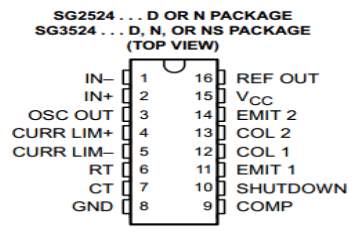
Fig 2.2-IC 3524 pin out
The output voltage of the single-phase inverter is roughly square wave and it can be controlled by means of pulse width Modulation. PWM technique is a control within the inverter and is also known as variable duty cycle regulation. This method of regulation employs variation of the conduction time per cycle to alter the RMS output voltage of the inverter. PWM oscillator is constructed using IC 3524. It consists of built in oscillator, comparators, error amplifiers and output control circuitry. In this IC, a 5V internal regulator is also provided. Internally, for the comparators one input is fed with a saw-tooth voltage and the other input is fed with a feedback monitoring voltage. As this inverter is configured in open loop operation PWM technique is not implemented here, there by output voltage is not regulated. The output voltage will be varied according to the load applied to the inverter. In our trail runs we found that the power system generates around 240V in no load condition, when the system is connected with rated load of around 70 watts, the voltage is fallen down by 220V.
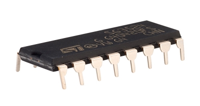
Fig 2.3-IC 3524 CHIP
The oscillator operates at a fixed frequency that is programmed by one timing resistor, RT and one timing capacitor, C; RT establishes a constant charging current for C. This results in a linear voltage ramp at C, which is fed to the comparator, providing linear control of the output pulse duration (width) by the error amplifier. The IC on board 5V regulator that serves as a reference, as well as supplying the internal regulator control circuitry. The internal reference voltage is divided externally by a resistor ladder network to provide a reference within the common mode range of the error amplifier. The output is sensed by a second resistor divider network and the error signal is amplified. This voltage is then compared to the linear ramp at C. The resulting modulated pulse out of the high-gain comparator then is steered to the appropriate output pass transistor (Q1 to Q2) by the pulse-steering flip-flop, which is synchronously toggled by the oscillator output.
2.3 DRIVER STAGE USING POWER MOSFETS
The driver stage designed with power mosfets is configured as class ‘B’ mode of push-pull amplifier. The advantage of class ‘B’ push-pull amplifiers are, it provides linear amplification. Apart from that the DC collector current is less than the peak AC current. Thus, less collector dissipation results and the efficiency increases. In the project work, center tapped transformer is used, which supplies two base currents of equal amplitudes but 1800 out of phase. There by in the first half cycle one MOSFET is off and the other MOSFET is conducting. Whereas in the second half cycle other MOSFET is conducting i.e., roles of power MOSFETS are reversed. The current in the conducting MOSFET flows through the upper half of the primary winding and the resulting time varying flux in the transformer core induce a voltage in the secondary winding. The voltage in turn produces the first half cycle of the current through the load. Similarly, when the MOSFET roles are changing, the flux in the transformer core in a direction opposite to the flux of previous half cycle of the load current. The final current of the load under these conditions is thus directly proportional to the signal current. In practice the load current would be extremely distorted near the zero crossing. This effect is called cross over distortion and is due to Gate-source voltage in MOSFET ‘VGS’ being zero when no signal is applied. However linear operation of the (transistor) MOSFET begins only when (base) Gate current is positive enough to cross the cut in voltage. To eliminate the distortion base-emitter junction is biased at approximately 0.7V. The result is class ‘AB’ rather than class ‘B’ operation but is very close to class ‘B’ mode. The bias is called the turn-on bias in practice, one often allows cross over distortion and relies on the transformer and internal and stray capacitors to filter it out.
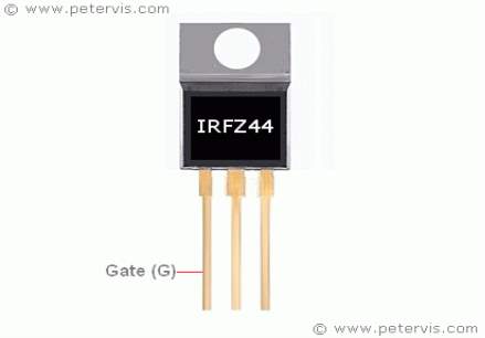
Fig 2.4-IRFZ44 MOSFET
2.4 MAIN OUTPUT TRANSFORMER
The main output transformer used in the driver stage is designed to deliver 0.35 amps current at the secondary. This is a step up transformer and the primary of this transformer is designed for 12V. This is a center tapped primary transformer and the primary is wounded with by-filler winding, i.e., the primary is wounded with two copper enameled wires simultaneously. Starting of the one winding is clubbed with ending of another wire to form a center tap. The advantage of adopting by-filler winding concept at primary side of the transformer is to maintain the accurate balance; there by the current flowing through both sections of primary remains equal.
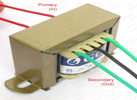
Fig 2.5- CENTR TAP TRANSFORMER
CHAPTER-3
CIRCUIT DIAGRAM
Fig 3.1- CIRCUIT DIAGRAM
3.1 DESCRIPTION
The complete circuit diagram shown above is explained in detail, as the oscillator circuit designed with SGS3524 IC playing major roll, the description is concentrated over internal structure of this device. Though the PWM technique is not implemented here, it is explained well because this device offers good regulated output at lower voltages. This IC is having 16 pins with all built-in features and this device is used for wide variety of applications like inverters, converters, switch mode power supplies, etc. The following are the key points.
It offers wide range frequency output; the frequency can be adjusted from 1Hz to 50 KHz. Pin numbers 6 & 7 are the frequency compensation pins, by connecting a resistor & capacitor externally to these pins, frequency can be set to required level. Here the required frequency is 50Hz, according to that the values of RT & CT (Resistor for timing & Capacitor for timing) can be selected. The capacitor is charged with constant current through a fixed resistor, there by regulated pulse output can be obtained either from common emitters or common collectors.
The pre-drive stage built in with the chip can able to supply a maximum current of 150ma from each output, hence additional pre-amplifier to drive the power stage is not required.
As this chip is designed to generate duel inverted outputs, drive stage is configured in push-pull amplifier. The advantage of using this amplifier is that the output transformer remains in energized condition continuously, thereby continuous output can be achieved from the power system.
This chip offers +5V regulated output from pin number 16; this can be used as a reference voltage for the control circuit. This voltage remains constant irrespective of variations in the input source.
In this IC pin number 10 is a shut-down pin, always it remains in zero state, whenever any control circuit generates high signal & it is fed to this pin, automatically output of this chip will become zero. (As the inverter designed here doesn’t contain any protection circuits, this facility is not used.)
Soft start provision is made in the oscillator circuit, such that the power system is protected burning from sudden switching. This circuit is designed with RC network and it is connected to 9TH pin, this is a compensation pin. When the power system is switched on, the capacitor charges through resistor, based on the values of capacitor and resistor, the capacitor will take some time to charge fully, until then the outputs will not be adjusted to its maximum levels.
The main important feature offered by this chip is varying the duty cycle very linearly. This can be done by varying the voltage at compensation pin through a potential dividing network designed with a preset.
Although many switching techniques can be employed to implement a switched mode power supply, either it is converter or inverter, the fixed frequency PWM system, a square wave pulse is normally generated to drive the switching transistor / MOSFETS ON or OFF. By varying the width of the pulse, the conduction time of the MOSFET is accordingly increased or decreased, thus regulating the output voltage. The PWM control circuit may be single ended, capable of driving a single MOSFET converter, such as Fly back or forward. If two or more MOSFET’S have to be driven, as with half-bridge or full-bridge circuits, a dual channel PWM circuit is necessary. In this project work dual inverted outputs are taken from the PWM IC, so that the drive stage is designed in push-pull configuration with two power Mosfets.
3.2 General description of an integrated PWM controller
In recent years, a number of integrated circuits have been developed which include all the functions necessary to build a PWM switching power supply in a single package with little addition of few external components. The basic building blocks of simple PWM controller and its associated waveforms are shown below.
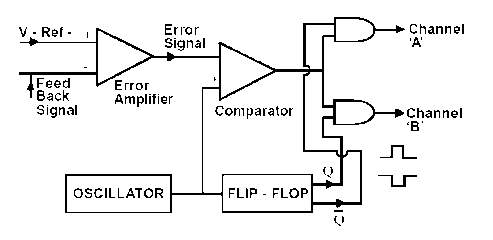
Fig 3.2- PWM CONTROLLER
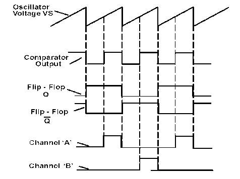
Fig 3.3-wave forms of PWM
An op-amp compares the feedback signal from the output of the power supply to a fixed reference voltage (V-ref). The error signal is amplified and fed in to the inverting input of a comparator. The non-inverting input of the comparator accepts a saw-tooth waveform with a linear slope, generated by a fixed frequency oscillator. The oscillator output is also used to toggle a flip-flop, producing square wave outputs Q and Q. The comparator square wave output and the Flip-Flop outputs are both used to drive the AND gates, enabling each output when both inputs to the gate are high. The result is a variable duty cycle pulse train at channels ‘A’ and ‘B’. In the above figure shows the output pulse width is modulated when the error signal changes its amplitude, as detected by the dotted lines. Normally the outputs of the PWM controller are externally buffered to drive the main power switching power MOSFETS. This type of circuit may be used to drive two transistors / MOSFETS or a single Transistor or MOSFET. The merits of a PWM controller are pro-found, including the programmable fixed frequency oscillator, Linear PWM section with duty cycle from 0 to 100 percent, adjustable dead time to prevent output transistor or MOSFET simultaneous conduction, and above all simplicity, reliability, and cost effectiveness. The PWM control circuit is IC 3524, which was designed to become the industry standard. These PWM controllers are the heart for the complete switching power supply design and may be used equally well in single ended or dual channel applications. The PWM comparator provides a means for the error amplifier to adjust the output pulse width from the maximum percent on time, established by the dead-time control input, down to zero, as the voltage at the feedback varies from 0.5V to 3.5V. The error amplifier outputs are active high. With this configuration, the amplifier that demands minimum output on time dominates control of the loop.
3.3 Internal block diagram of PWM chip SG3524
The oscillator output pulse also acts as an inhibiting pulse to make sure that both the transistors are never turned ON simultaneously. The duration of this pulse is determined by the value of CT.
The pin 11 and 14 are connected to the TIP transistor for driving the transformer. T1 is a 12-0-12 V primary, 220V secondary, 300VA transformer.
When signal at pin 14 is high, upper transistor is switched ON and current flows from the +12V source via the upper half of the transformer to the ground.
When 11 of the IC pin goes high, lower transistor gets switched ON and current flows from the +12V source via the lower half of the transformer primary and sinks to the ground.
Thus we got positive and negative half cycles of 220V AC supply.
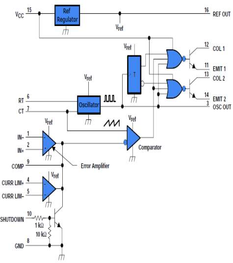
Fig 3.4- internal block diagram of 3524
3.4 The following are the salient features of PWM controllers
1) Fixed frequency operation, user programmable by a simple RC Network.
2) A variable slope Ramp generator for constant volt per second operation, providing open loop line regulation and minimizing, or in some cases eliminating the need for feedback control.
3) A drive switch for low current start-up with direct off-line bias.
4) A precision reference generator with internal over voltage protection
5) Under voltage and over current protection including programmable shutdown and re-start.
6) A high current, single ended PWM output optimized for fast turn-off of an external power switch.
7) Logic control for pulse commendable or DC power sequencing
In this IC 3524, the internal linear saw-tooth oscillator is frequency programmable by resistor ‘RT’ and capacitor ‘CT’ (0.1 uF) which are connected to Pins 6 and 7 of the IC. To tune the frequency, in addition to 100K Resistor, 50K potentiometer is also connected. The oscillator frequency f out = 1 / RT CT. The Ramp voltage swings approximately 2.5V to change the comparator output from 0 to 1, by comparing it to either one of two control signals, i.e., the error amplifier output or the current limit amplifier output. The error amplifier input range exceeds beyond 5V, eliminating the need for a pair of dividers, for 5V outputs. To provide a reference voltage to the error amplifier, the on board 5V regulator provides with an accuracy of ± 1 percent. In this, the output pulse width modulation is accomplished by steering the resulting modulated pulse output of the high gain comparator to the PWM latch along with the pulse steering Flip-Flop, which is synchronously toggled by the oscillator output.
The PWM latch insures, freedom from multiple pulsing within a period, even in noisy environments in addition, the shutdown circuit feeds directly to this latch, which will disable the outputs within 200 n. sec. of activation. The current limit amplifier is a wide-band, high gain amplifier, which is useful for either linear or pulse by pulse current limiting in the ground or power supply lines. Its threshold is set at 200mv. An under voltage lockout will disable the internal circuitry, except the reference, until the input voltage is 8V. This action holds stand by current low until turn on, simplifies the design of low power, off line switchers. These are the advantages of this versatile controller, there by this can be used in a variety of Isolated or non-isolated switching power supplies like inverters or converters. Hence, in this project work, this controller is selected for usage and the inverter is designed using this PWM controller.
The basic concept of pulse width Modulation is given below; In the case of op-amp, when it is configured in open loop configuration, the output will go to either +V sat or –V sat due to its high gain. The switching of +V sat and –V sat is, whenever the inverting input is slightly more than Non-inverting input voltage, the output will be in –V sat. i.e., if inverting input dominates Non-inverting input, immediately the output will be –V sat. The V sat will be V ± 1.5V. Similarly, if the non-inverting voltage is slightly more over the inverting input voltage, the output voltage will be +V sat. Thus, the output will be only either +V sat or –V sat. Now we will give RAMP or saw-tooth voltage to the non-inverting input and the feedback or some variable DC voltage will be given to the inverting input and we will see how the output voltage changes. There by the output pulse width modulation takes place depending upon the feedback voltage. These are best described with the waveforms, which are given below.
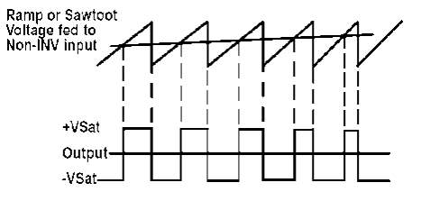
Fig 3.5 output waveforms from ramp signal
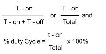
As we see the output, it’s on / off periods is changing every cycle depending up on the feedback voltage. This concept is called pulse width Modulation. Also this concept is called duty cycle variation. Duty cycle is equals to
The following is the circuit diagram of PWM Oscillator
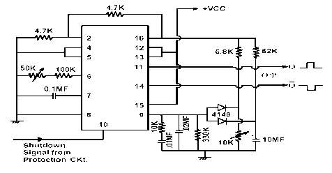
Fig 3.6- PWM oscillator
In the above circuit, the inverting input of Error amplifier (Pin No.2) is fed from V ref, built in 5V regulator through a voltage divider of two 4.7K resistors. This +5V regulator is available inside the IC.
The voltage at Pin NO.2 is 5V x 4.7K / 4.7K + 4.7K = 2.5V.
The current limit amplifier is not used at present, hence are connected to ground. The frequency of the internal Oscillator is adjusted with RT and CT. The Ramp generator is internally connected inside the IC to the pulse width Modulator. For details related to the internal details of the IC, it was described in the Chapter Hardware details. To shutdown the IC, i.e., to disable the PWM output, such as excess current drawn by load, the high signal to shutdown pin disables the output, and thereby inverter is protected from overload. The built in PWM generator, the complementary ‘Q’ and ‘Q’ output from the internal Flip-Flop and passes through internal NOR gates clocked by the internal Oscillator. These outputs are at 50Hz frequency (approximately) PWM output, are further amplified using class ‘B’ push-pull stages. The Pin .9 compensation input is connected with soft start circuit. This makes the PWM regulator to generate the output, when the switch ‘ON’ the unit, slowly, thereby it avoids false triggering of the protection circuits. The time constant RC is designed with 82K x 10MF = 820m sec. To reduce this delay a 6.8K and 10K potentiometer are connected as a voltage divider.
By varying the voltage at Pin no.9 (Compensation Pin) output duty cycle can be changed, for this purpose 10K Pot (variable resistor) is connected between Pin NO.9 and ground. By varying the resistance reference voltage at compensation pin also can be varied very linearly. Hence by varying duty cycle output voltage can be controlled.
3.5 Description about drive stage
As described in previous chapters, the drive stage is configured as push-pull amplifier. The main purpose of this amplifier is to amplify the voltage and current levels to the required level; the required level is to drive a 60Watts load, which may consume a maximum current of 300ma at 220V ac. Therefore to be safe side, this amplifier is designed to generate 350ma maximum. In a voltage amplifier, the output voltage is many times greater than the input voltage. Similarly current is also amplified. The components in an amplifier are selected to give high gain or amplification which is the ratio of the output voltage to input voltage. The output of the oscillator, where ac signal is produced at low voltage and low currents is extremely small, and need amplification before being really useful to drive the motor. A power amplifier may have voltage gain, but the main consideration is the power output which is the product of current and voltage.
In a class ‘B’ push-pull amplifier consists of two identical drive stages at output circuitry, designed with power mosfets drives the main transformer. These mosfets are excited with equal but opposite (180 degrees out of phase) voltages from the input signal. When operated in this manner, one of the mosfet amplifies the positive half cycles of the signal voltage while the other mosfet amplifies the negative half cycles. The amplified half cycles are then combined in the output transformer in such a manner as to produce an amplified reproduction of the input voltage and current. In actual practice, the two mosfets are switched in a sequence one after another according to the biasing signals produced by the oscillator. This avoids crossover distortion. The mosfets are conducted one after another according to the time period, based on this frequency produced by the oscillator, a gap between the time when one mosfet shuts off and the other is turned on and this produces a clipping effect on the output voltage. In this condition output is distorted, this type of distortion is called crossover distortion.
The following is the circuit diagram driver stage.
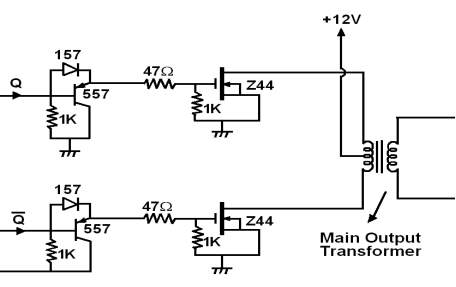
Fig 3.7- Driver circuit
In the above circuit, BC 557 general-purpose PNP switching transistors are used to drive the Power MOSFETS. The PWM outputs of regulator, which are obtained from emitters of A and B transistors (provided inside IC) are amplified to drive the load. For this, class ‘B’ push-pull stages are used in pre-driver stage and driver stage. Thus, a great deal of this distortion introduced by the Non-linearity of the dynamic transfer characteristic may be eliminated by push-pull configuration. In this case when the signal on one MOSFET is positive, the signal on other is negative by an equal amount. The advantage of push-pull amplifier is it will eliminate even harmonics. The fact that the output current contains no-even-harmonic terms means that the push-pull possesses ‘Half wave’ or ‘mirror’ symmetry in addition to the zero axis symmetry. Because no even harmonics are present in the output of a push-pull amplifier, such a circuit will give more output per active device for a given amount of distortion. For the same reason, the push-pull arrangement is used to obtain less distortion for a given power output per MOSFET. Another advantage of push-pull arrangement is that the DC components of the collector current oppose each other magnetically in the transformer core. This eliminates any tendency toward core saturation and consequent Non-linear distortion that might arise from the curvature of the transformer magnetization curve. Another advantage is effects of ripple voltages that may be contained in the power supply because of inadequate filtering will be balanced out.
The advantage of using power MOSFETS, when compared with bipolar power transistors, because of its input high impedance No load current can be reduced and efficiency can be increased.
CHAPTER-4
POWER SOURCE DESCRIPTION
4.1 BATTERY
This device can be called as chemical voltage source; a chemical voltage source is one of the most important sources of electrical energy. It is a self contained voltage source and does not need any outside energy. When the battery is discharged it is supposed to be charged with suitable power source either from solar panel or from mains supply, i.e. single phase conventional energy source. The electrical energy supplied by a chemical source of voltage is produced by chemical action within the source itself. Chemical voltage sources normally exist in the form of batteries and cells of various types. These batteries are extensively used for mobile applications.
Whenever the power system is energized and it is loaded, the required power to drive the load is generated from the inverter & it is powered through battery. Here heavy duty battery of 7.5AH (Ampere Hour) current rating is used for long back-up time, means when average power is considered the battery can withstand up to one hour. This is a maintenance free battery built in with a group of cells combined together to increase the voltage and current to the required level. A cell or battery is classified as a ‘primary’ or ‘secondary’ depending up on the manner in which the chemical energy is converted in to electrical energy. The primary cell cannot be re-charged, it is a type use and through concept battery. A secondary cell must be charged with electrical energy first to enable it to convert the chemical energy into electrical energy. Because of its action of storing energy supplied to it, a battery consisting of secondary cells is often called a storage battery. Here in this project work this kind of re-chargeable storage battery is used. As it is a prototype module, the battery used here can withstand for one hour, but for real applications heavy duty battery can be used for long back-up.
As the inverter operates at 12V DC, here 12V DC lead acid re-chargeable battery is used and it is accommodated along with the power system. As the inverter is loaded with 60watts lamp, it consumes nearly 6Amps continuous current from the battery. To calculate the backup time, first we must calculate the overall power consumption, it is assumed as 6A, therefore back-up time = battery rating / consumption, i.e. 7.5/6 = 1.25 hours approximately. In general the average power of battery is considered as 20% less than the rating. According to this equation back up time is depends up on the power consumption & average power of the battery, there by back-up time can be defined as 1 hour only.
Batteries are maintenance free sealed lead acid rechargeable batteries. The batteries are having excellent economy stability and superior output. Various characteristics have been improved such as leak proof, overcharging and over discharging. This compact & powerful sealed lead-acid battery with higher performance can be used as a power source for portable instruments and also for power backup use. Batteries are now being used in a wide range of applications.
4.2 Charging method
These Batteries are maintenance free. There is no need to add water. Battery performance and service life are greatly affected by the charging method. There are various different charging methods: constant voltage charging, constant current charging, tapered current charging and some combination systems. Batteries can be charged by any of those methods. However, constant voltage charging combined with limited current is recommended for obtaining maximum capacity and service life together with acceptable recharge times and economy. Here the battery is charged with constant voltage source.
Here Solar Energy is used; the following is the description of solar power source
In today’s climate of growing energy needs and increasing environmental concern, alternatives to the use of non-renewable and polluting fossil fuels have to be investigated. One such alternative is solar energy. Solar energy is quite simply the energy produced directly by the sun and collected where required. The sun creates its energy through a thermonuclear process that converts about 650,000,000 tons of hydrogen to helium every second. The process creates heat and electromagnetic radiation. The heat remains in the sun and is instrumental in maintaining the thermonuclear reaction. The electromagnetic radiation (including visible light, infra-red light, and ultra-violet radiation) streams out into space in all directions.
Only a very small fraction of the total radiation produced reaches the Earth. The radiation that does reach the Earth is the indirect source of nearly every type of energy used today. The exceptions are geothermal energy, and nuclear fission and fusion. Even fossil fuels owe their origins to the sun; they were once living plants and animals whose life was dependent upon the sun. Much of the world’s required energy can be supplied directly by solar power. More still can be provided indirectly. The practicality of doing so will be examined, as well as the benefits and drawbacks.
Due to the nature of solar energy, two components are required to have a functional solar energy generator. These two components are a collector and a storage unit. The collector simply collects the radiation that falls on it and converts a fraction of it to other forms of energy (either electricity and heat or heat alone). The storage unit is required because of the non-constant nature of solar energy; at certain times only a very small amount of radiation will be received. At night or during heavy cloud cover, for example, the amount of energy produced by the collector will be quite small. The storage unit can hold the excess energy produced during the periods of maximum productivity, and release it when the productivity drops. In practice, a backup power supply is usually added, too, for the situations when the amount of energy required is greater than both what is being produced and what is stored in the container. Lithium Ion batteries normally have an anode made of graphite. Using an anode made of silicon (Si) can increase the capacity up to 6 times, because the Si-anode can accept much more Lithium-ion than a graphite-anode. A problem was that the Si-anode expands 300–400% when charged. The Si-anode had only a small lifespan. Researchers of the university of Stuttgart (institute of photovoltaic (IPV), Prof. Dr. Jorgen H. Werner and his team) found a way making the Si-anode porous, so that accepting so many Lithium-ion will no longer increase the volume of the Si-anode, so that the lifespan of the battery with Si-anode is now four times higher than batteries with graphite-anode. The battery is ready for production.
John B. Goodenough, one of the inventors of lithium-ion battery, recently (2017) helped develop the glass battery, a developmental battery with a glass electrolyte that is reported to exceed current lithium-ion batteries in energy density, operating temperature range, and safety.
CHAPTER-5
DESCRIPTION OF TRANSISTORS
A transistor is device used to amplify or switch electronic signals and electrical power. It is composed of semiconductor material usually with at least three terminals for connection to an external circuit. A voltage or current applied to one pair of the transistor’s terminals controls the current through another pair of terminals. Because the controlled (output) power can be higher than the controlling (input) power, a transistor can amplify a signal. Today, some transistors are packaged individually, but many more are found embedded in integrated circuits.
The transistor is the fundamental building block of modern electronic devices, and is ubiquitous in modern electronic systems. Julius Edgar Lilienfeld patented a field-effect transistor in 1926 but it was not possible to actually construct a working device at that time. The first practically implemented device was a point-contact transistor invented in 1947 by American physicists John Bardeen, Walter Brattain, and William Shockley. The transistor revolutionized the field of electronics, and paved the way for smaller and cheaper radios, calculators, and computers, among other things. The transistor is on the list of IEEE milestones in electronics, and Bardeen, Brattain, and Shockley shared the 1956 Nobel Prize in Physics for their achievement.
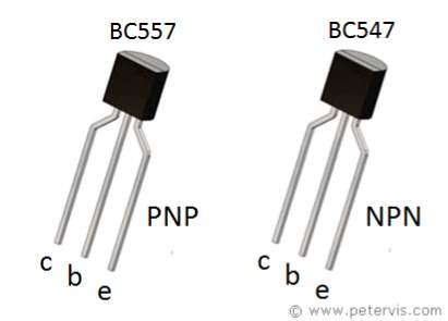
Fig 5.1 transistors
5.1 Transistor as a switch
Transistors are commonly used in digital circuits as electronic switches which can be either in an “on” or “off” state, both for high-power applications such as switched-mode power supplies and for low-power applications such as logic gates. Important parameters for this application include the current switched, the voltage handled, and the switching speed, characterized by the rise and fall times.
In a grounded-emitter transistor circuit, such as the light-switch circuit shown, as the base voltage rises, the emitter and collector currents raise exponentially. The collector voltage drops because of reduced resistance from collector to emitter. If the voltage difference between the collector and emitter were zero (or near zero), the collector current would be limited only by the load resistance (light bulb) and the supply voltage. This is called saturation because current is flowing from collector to emitter freely. When saturated, the switch is said to be on.
Providing sufficient base drive current is a key problem in the use of bipolar transistors as switches. The transistor provides current gain, allowing a relatively large current in the collector to be switched by a much smaller current into the base terminal. The ratio of these currents varies depending on the type of transistor, and even for a particular type, varies depending on the collector current. In the example light-switch circuit shown, the resistor is chosen to provide enough base current to ensure the transistor will be saturated.
In a switching circuit, the idea is to simulate, as near as possible, the ideal switch having the properties of open circuit when off, short circuit when on, and an instantaneous transition between the two states. Parameters are chosen such that the “off” output is limited to leakage currents too small to affect connected circuitry; the resistance of the transistor in the “on” state is too small to affect circuitry; and the transition between the two states is fast enough not to have a detrimental effect.
5.2 Transistor as an amplifier
The common-emitter amplifier is designed so that a small change in voltage (Vin) changes the small current through the base of the transistor; the transistor’s current amplification combined with the properties of the circuit means that small swings in Vin produce large changes in Vout.
Various configurations of single transistor amplifier are possible, with some providing current gain, some voltage gain, and some both.
From mobile phones to televisions, vast numbers of products include amplifiers for sound reproduction, radio transmission, and signal processing. The first discrete-transistor audio amplifiers barely supplied a few hundred milliwatts, but power and audio fidelity gradually increased as better transistors became available and amplifier architecture evolved.
Modern transistor audio amplifiers of up to a few hundred watts are common and relatively inexpensive.
CHAPTER-6
HARDWARE DETAILS
The IC’s and other important components used in this project work are procured from the Hyderabad Electronics Market. The details or data sheets of the IC 3524 are down loaded from the Internet.
The following are the IC and other important components used in this project work
1) SG 3524 Regulating Pulse Width Modulation
2) Z44 Power MOSFET
3) Voltage Regulator
4) Mains output transformer
5) Current Transformer
The required PCB’S (Printed Circuit boards) for the project work fabricated by SUN RISE CIRCUITS, Kushaiguda Industrial Estate, Hyderabad. Kushaiguda Industrial Estate is very famous for fabricating the Industrial grade PCB’s.
CHAPTER-7
RESULTS OF THE PROJECT
Fig 7.1 CHANNEL-1 output
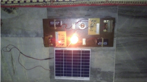
Fig 7.2 CHANNEL-2 output
CHAPTER-8
CONCLUSIONS
The project work “Single phase multi-channel Inverter” is successfully designed tested and a demo unit is fabricated. Since it is a demonstration unit, two similar type of low power inverters are designed which can able to deliver a maximum current of 350 milliamps each at 220V at the system output. But for the practical applications, a higher rating inverter can be designed which can be used for the multiple applications simultaneously.
As the power system is designed to deliver less power, protection circuits are not included. In general the higher rating inverters are equipped with thermal protection over load cut off circuits. With the help of a load monitoring circuit often designed with CT, the load applied to the inverter will be monitored continuously, whenever the load exceeds more than the rated value, immediately system will be shut-down. After reducing the load and by activating the reset button power will be resumed. Similarly thermal protection system also protects the power system burning due to over temperature. These are the features to be added in our feature work.
In this project work solar energy is not used for charging the battery, but if it is used it can be said as this is one type of best method for charging the battery, which comes under non-conventional method of power generation. Sun is the primary source of the energy; the energy radiated by the sun is in the form of electro-magnetic waves. The winds produced by the nature are used to drive small power generators called as windmills. Such generators are also can be used for charging the batteries. The great advantage of using the above two methods in non-conventional energy resources, the energy produced by these two methods is plentiful, inexhaustible, non-polluting and it does not require in a operator and also does not require any maintenance. These kinds of systems are very rugged systems so that during the long run they may not create any problems.
CHAPTER-9
REFERENCES
In order to select a suitable topic for the project, few books are referred. The list is as follows:
Power systems By: J.B. GUPTA
Solar Energy Utilization By: G.D. Rai
Power from the Sun – A practical guide to solar electricity by Dan Chiras
Wind and solar power systems By: Mukund R. Patil
Solar electricity hand book By: Michael boxwel
National Semiconductors (Company Catalog)
Power Electronics By: P.C. Sen.
http://www.petervis.com/electronics/bc547/bc547/bc547
https://en.wikipedia.org/wiki/Solar_panel
http://www.circuitstoday.com/wp-content/uploads/2011/08/PWM-inverter-circuit.png
https://en.wikipedia.org/wiki/Power_MOSFET#/media/File:Bv_rdson.png
Cite This Work
To export a reference to this article please select a referencing stye below:
Related Services
View all


Related Content
All TagsContent relating to: "Energy"
Energy regards the power derived from a fuel source such as electricity or gas that can do work such as provide light or heat. Energy sources can be non-renewable such as fossil fuels or nuclear, or renewable such as solar, wind, hydro or geothermal. Renewable energies are also known as green energy with reference to the environmental benefits they provide.
Related Articles

DMCA / Removal Request
If you are the original writer of this dissertation and no longer wish to have your work published on the UKDiss.com website then please: