VLSI Implementation of a Key Distribution Server based Data Security Scheme for RFID
Info: 19040 words (76 pages) Dissertation
Published: 24th Feb 2022
Abstract
RFID Technology is now a globally accepted technology which is rapidly emerging in every field of science and applications. It’s excellent feature of very fast auto identification without line of sight has made it popular in different areas of wire-less communication based system. But, during data transmission/exchange, security of personal or confidential data, it exposes serious threats to the security and privacy of individuals and organizations. Data security for RFID technology is now a mandatory condition to be provided by the manufacturer for better customer support and services. In this paper, we have proposed a security scheme which introduces a trusted Key management system. In this system, not a single key but several keys will be maintained, controlled and provided by the Key distribution server system (KDSS). It will be extremely useful for military persons in remote places where it is useful to identify specific item or guide to right route. Data will be encrypted using different programmable cellular automata (PCA) rules which is also provided with the key by the server.
CHAPTER 1: INTRODUCTION
1.1 Introduction
There was a great deal of interest in RFID from researchers, awesome arrangement of enthusiasm for RFID from scientists, engineers and scholarly organizations in the 1970s and RFID technology achieve its momentum. Commercial applications of RFID enter mainstream in early 1980’s and RFID emerged as wide applications in 1990’s period. Recently, advancements proceeded in the 1990s with incorporated circuit improvement and size diminishment until microwave RFID labels were decreased to a solitary coordinated circuit. Impressive work is being undertaken in many commercial applications. There are now more than 350 patents have been registered with the US Patent Office related to RFID and its applications. It is also used for access control. different applications under thought, for instance, the consolidation of RFID labels into essential records, for example, birth endorsements, driver licenses, instructive declarations, original copies, therapeutic enlistments et cetera. Truth be told it is utilized as a part of any archive where validness and veracity are basic.
RFID devices must be very low cost to provide successful globalization in every field. To cut down the cost, these are generally passive devices with limited functionality. Affordable tags having only 500–5000 gates cannot perform standard cryptographic operations necessary for privacy and security. Advanced Encryption Standard (AES) algorithm for data security requires almost 20,000 to 30,000 entryways to deal with the cryptographic security. Security for the present era of detached RFID labels along these lines speaks to an extensive test.
RFID (Radio frequency identification)
RFID labels, or just “labels”, are little transponders that react to inquiries from a peruser by remotely transmitting a serial number or comparable identifier. They are intensely used to track things underway conditions and to mark things in general stores. The protest of any RFID framework is to convey information in reasonable transponders, by and large known as labels, and to recover information, by machine-comprehensible means, at an appropriate time and place to fulfill specific application needs. Information inside a tag may give distinguishing proof to a thing in make, merchandise in travel, an area, the personality of a vehicle, a creature or person. By including extra information the prospect is accommodated supporting applications through thing particular data or guidelines promptly accessible on perusing the tag. For instance, the shade of paint for an auto body entering apaint splash region on the generation line, the set-up directions for an adaptable assembling cell or the show to go with a shipment of merchandise. A framework requires, notwithstanding labels, a methods for perusing or examining the labels and a few methods for imparting the information to a host PC or data administration framework. A framework will likewise incorporate an office for entering or programming information into the labels, if this is not embraced at source by the producer. Regularly a reception apparatus is recognized as though it were a different piece of a RFID framework. While its significance legitimizes the consideration it must be viewed as an element that is available in both perusers and labels, fundamental for the correspondence between the two.
Recurrence Bands
RFID labels fall into three areas in regard to recurrence: Low recurrence (LF, 30 – 500kHz) High recurrence (HF, 10 – 15MHz) Ultra high recurrence (UHF, 850 – 950MHz, 2.4 – 2.5GHz, 5.8GHz) Low recurrence labels are less expensive than any of the higher recurrence labels. They are sufficiently quick for most applications, however for bigger measures of information the time a tag needs to remain in a perusers range will increment. Another favorable position is that low recurrence labels are slightest influenced by the nearness of liquids or metal. The hindrance of such labels is their short perusing range. The most widely recognized frequencies utilized for low recurrence labels are 125 – 134.2 kHz and 140 – 148.5 kHz. High recurrence labels have higher transmission rates and ranges additionally cost more than LF labels. Keen labels are the most widely recognized individual from this gathering and they work at 13.56MHz
Principles
The extensive variety of conceivable applications requires a wide range of sorts of labels, frequently with clashing objectives (e.g. minimal effort versus security). That is reflected in the quantity of benchmarks. A short rundown of RFID guidelines takes after: ISO 11784, ISO 11785, ISO 14223, ISO 10536, ISO 14443, ISO 15693, ISO 18000. Take note of that this rundown is not comprehensive. Since the RFID innovation is not straightforwardly Internet related it is not amazing that there are no RFCs accessible. The current buildup around RFID innovation has brought about a blast in licenses. As of now there are more than 1800 RFID related licenses issued (from 1976 to 2001) and more than 5700 licenses portraying RFID frameworks or applications are accumulated.
RFID Systems
A RFID peruser and a couple labels are when all is said in done of little utilize. The recovery of a serial number does not give much data to the client nor does it monitor things in a generation chain. The genuine energy of RFID comes in blend with a backend that stores extra data, for example, depictions for items and where and when a specific tag was filtered. As a rule a RFID framework has a structure as delineated in figure 2. RFID perusers check labels, and after that forward the data to the backend. The backend all in all comprises of a database and an all around characterized application interface. At the point when the backend gets new data, it adds it to the database and if necessary plays out some calculation on related fields. The application recovers information from the backend. As a rule, the application is gathered with the peruser itself. An illustration is the checkout point in a grocery store (Note that the given case utilizes standardized identifications rather than RFID labels since they are more typical; notwithstanding, the framework would carry on in the very same way if labels were utilized). At the point when the peruser examines the scanner tag, the application utilizes the determined identifier to query the present cost. Likewise, the backend additionally gives markdown data to qualifying items. The backend likewise diminishes the quantity of accessible results of that kind and advises the supervisor if the sum falls beneath a specific edge.
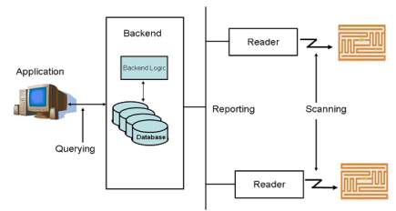
Figure 1: A rearranged RFID framework
Security
The normal multiplication of RFID labels into the billions has raised numerous protection and security concerns. A typical concern is the loss of protection when organizations check labels to gain data about clients and after that utilizing information mining methods to make singular profiles. This area portrays conceivable situations where RFID labels can be abused. At that point it depicts what instruments exist to crush those dangers or if nothing else make them harder to execute. After that the area focuses on assaults that are coordinated against RFID frameworks. As RFID innovation turns out to be more modern and thing level labeling guarantees more control and vast funds in the inventory network administration, organizations are labeling things inside their creation procedure. To expand the advantages organizations begin to require their providers to mark all things conveyed to the organization.
Hostile to RFID activists made a couple of situations to show conceivable endeavors if no precautionary measures are taken. The most widely recognized one the unapproved checking of labels keeping in mind the end goal to make client profiles. Different situations are checking the prescription a man is conveying to guess what sickness the individual may endure, or a mugger examining a horde of individuals and singling out a man conveying numerous significant things (even cash, if labeled as proposed). In the event that labels are supplanting Mastercards listening in turns out to be additionally an issue and should be tended to. The previously mentioned issues are security concerns, yet they are not by any means the only issue. Validation is likewise required. For instance, more current labels have rewritable memory accessible to store additional data amid the generation procedure. In the event that stores depend on that data to decide the business cost for instance, mind must be taken so clients don’t change the sort of the thing to a less expensive one utilizing convenient perusers. Additionally the execute summon, a system to for all time debilitate a tag, must be shielded from unapproved get to. As of late a paper brought a few worries up in the RFID people group that asserted that phones can be reinvented to handicap HF labels. On the off chance that that labels convey individual data, (for example, therapeutic history, Mastercard numbers) a peruser must be confirmed and approved before it is permitted get to the information. In the past illustrations the peruser needs to confirm to the tag, there are likewise situations when the tag needs to validate to the peruser, for instance to identify manufactured labels.
Verification
The objective of verification is to ensure that an element is the thing that it cases to be. With regards to RFID it implies that labels can recognize approved perusers from different perusers. This should be possible by utilizing encryption with a preshared key. The other path around is a great deal more troublesome. Here a peruser needs to guarantee that the label it is perusing is not modified or duplicated. Incidentally it is a somewhat difficult issue. Encryption is commonly used to set up some trust between both members of a discussion (notwithstanding protection). The principle issue for this approach is simply the exceptionally constrained assets on the label itself. Most labels have just a couple of hundred rationale entryways, yet most encryption plans require a few thousand doors. A few lightweight encryption conventions have been executed, for example, AES. In any case, it has been demonstrated that they have numerous feeble focuses and can be broken. For instance the Digital Signature Transponder (DST) calculation ensuring the Speed Passwas broken by specialists from the John Hopkins University [Bono05] permitting them to bring gas with a cloned speed-pass. Notwithstanding shortcomings in encryption calculations themselves, RFID labels give unwillingly more help to break those calculations. Numerous present labels “send out” lower layer properties, for example, the power and timing of the back scattered flag and the preparing postpone which contrast from contribution to enter. That additional data can be utilized to break encryption considerably more effectively. More up to date labels attempt to settle that issue by two free circuits for calculation and back dispersing. The expectation that future eras of RFID labels will give more assets to actualize more grounded encryptions won’t not materialize. The purpose behind this is there is (and there might dependably be) the value weight that requests less expensive labels for thing level labeling. What’s more, more assets mean higher costs.
1.2 Objective
The goal of the project is to study and analysis of Key Distribution Server based Data Security Scheme for RFID framework utilizing VLSI Technology.
1.3 Motivation
In this Project affordable tags having only 500–5000 gates cannot perform standard cryptographic operations necessary for privacy and security. Advanced Encryption Standard (AES) algorithm for data security requires almost 20,000 to30,000 entryways to deal with the cryptographic security. Security for the present era of aloof RFID labels in this way speaks to an extensive test.
1.4 Issue Statement
In this during data transmission/exchange, security of personal or confidential data, it exposes serious threats to the security and privacy of individuals and organizations.
1.5 Proposed Methodology
In a security zone like defence, it is more important to deliver right message to right person without intimating others. Extreme secret is maintained during data reporting related to defence plan or operating manuals of specific weapons for special activities.
1.6 Scope and Outline of thesis
A novel trusted key distribution server based high security scheme for RFID based system has been proposed and implemented in this work. Where communication system is abruptly disturbed/ unavailable, this security scheme provides ultimate security of information and person.
1.7 Main Contribution
Application of RFID is now in advance stage in defence and military and other high ends, this scheme are useful to protect data and access data securely. FPGA implementation of this scheme provides a single chip solution with minimum hardware, high speed operation with negligible power consumption.
CHAPTER 2: LITERATURE SURVEY
Mubarak et al present a review of the RFID system towards security, trust and privacy. According to them, most of the RFID work discusses security and privacy as two different solutions. Their approach presents security, trust and privacy as a one complete RFID solution. This also helped them to sort out the issues related with tag tracking and privacy of the data on the tag. The combination of all the three approaches will help in protecting the data within the system, i.e., when the data is at rest and also when it’s within the communication channels. In their approach, they propose the use of a lightweight encryption solution such as modified AES or ECC can be used to encrypt the data. This will help in providing the security aspect of their proposed approach when the data is in motion through the communication channel. In order to provide the security to data at rest, they propose to make the use of Trusted Platform Module (TPM).
Based on their previous work related to mutual attestation and integrity verification, the authors propose to provide the trust component of their proposed protocol. They make the use of process of Attestation which is similar to challenge response protocol between the platform to be verified and already verified platforms. The TPM provides the integrity values that need to be verified. The privacy part of the proposed approach is given by the use of anonymizer. An annonymizer is a device that annoymizes each tag id when it participates in the communication process. The published work is a first of its kind which has taken into account all the three aspects i.e. security, trust and privacy and presented them as a one solution. The major drawback with this approach is that they did not provide any kind of results or proof of concepts to support their claims. The discussed approach is a theoretical one and has not been implemented. The authors are taking up the best of the already available optimal solutions for each of security, trust and privacy and trying to come up with the optimal global solution. This approach does not always provide with the best solution.
Kim et al proposed a lightweight RFID Authentication protocol with a new set of keys generated at each step of the communication process. The problem they tried to address is related to location tracking and user privacy. They make the use of AES for authentication. The symmetric keys are updated with each communication through Random Number Generator generated by the Tag, Reader and the Server. This results in a new set of keys for encryption for each communication. They have assumed that the communication channel between the reader and the server is safe where as the communication medium between the tag and the reader is assumed to be open to attack by the adversary. The proposed protocol is broken into two stages.
The first stage is known as the initialization stage. The tag and the server have the same symmetric key at start. The reader and the tag have the same secret number and this would help the tag to authenticate the server. This approach helps in mitigating several attacks such as eavesdropping, replay attack and location tracking. This is due to the random number generated through the Pseudo Random Number Generator. Since it is not possible to get the previous key and the key changes for new communication, it gets difficult to use the keys to get a pattern. Different messages are transmitted in each communication and also the tag identification is never sent in open. This approach is safe against tag tracking problem. The major drawback of this approach is that it uses a static number ‘m’ across all the tags and the readers. This number helps the tag to authenticate reader through a simple encryption XOR operation. This number remains static throughout the life time of the system. If an adversary gets hold of this number, this will eventually lead to compromising the security of the whole system and eventually bring it down. Another problem with the proposed approach is that it suffers from the de synchronization attack. The random number generators are updated with each message assuming that other two entities will also update their random number generators in successive messages. The problem will arise if the message is lost during the transmission or an adversary blocks the messages from reaching the next entity. This will lead to de synchronization of random number generators between the three entities and they would not be able to decrypt the messages being received. This will result in failing to authenticate even a genuine set of readers or tags or both by each other.
Trecketal proposed two non-deterministic light weight protocols for security and privacy in RFID systems. These proposed protocols are known as non deterministic because when a reader gets a response from a tag for a challenge, the expected values of the response are not unique nor discrete but they lie in an interval; this puts the calculation overhead on the reader and the backend system. The interval range is predefined and the tag and the reader share a same secret numbers which remains static. The tag is assumed to store up to four different numbers. These numbers are basically the time stamps of the reader that has inquired the tag. These protocols are suitable for single as well as multiple tag environments. When the reader queries the tag, the tag computes the random number from the given time stamps and concatenates it with the secret number and sends it back to the reader
On receiving the message, the reader calculates the expected response from the given interval and compares the response with received message. If the match occurs, the tag is said be an authentic one. In the second protocol, the reader sends out the challenge to the tag. The tag checks if the received message is already present in the list of stored numbers. If the challenge is a new one, the tag stores it in its stack, otherwise it is discarded. Based on the received challenge, the tag computes a random number Δr. This random number is basically the difference between any two stored numbers in a tag. It concatenates the obtained result with the already stored secret number s. This result is further XORed with Δr. The reader on receiving this message calculates Δr and then concatenates it with secret number s.
This result is Xored with the range of Δr’s obtained from the set of timestamps the reader has already stored with it. The process continues until the match occurs. The proposed approach helps in mitigating several well known attacks such as man in the middle, passive eaves dropping and the replay attack. The major drawback with this approach is the use of time stamps. This is a serious issue if the different readers having different values of time stamps are used to query a same tag. These protocols will face serious issue if they are deployed in a multi tag and a multi reader environment. These proposed approaches may also suffer from a de synchronization attack. These approaches put up a lot of computational strain on the readers. This could potentially decrease the performance in a scenario where several tags are read by the reader at the same time. Furthermore, the shared secrets remains static throughout the system i.e. it’s same for all the readers and the tags. If an adversary gets hold of this shared secret, it will potentially compromise the security of the whole system.
Lopez et al proposed an authentication scheme for a low cost RFID tags operating under the EPC global Framework. In 2006, EPC global and the International Organization for standards specified universal standards for low cost RFID tags. The major concern with these specifications was that the security issues were not properly addressed. Konidala et al tried to address this issue with their proposed scheme. But Lim an Li showed that a passive eavesdropping attack can be launched on this scheme and thus it could lead to the password recovery if the eavesdropping can be done through multiple sessions and the packets can be reverse engineered.
Konidala et al tried to mitigate the problem in the extended version of their protocol but it again failed for almost a similar kind of attack. Lopez et al tried to mitigate these problems in the third version of the protocol known as M3 Authentication Protocol. This scheme is basically an extension of Konidala and Kim’s scheme. The main focus of the new proposed approach is to provide mutual authentication between the RFID tag and the RFID reader. They have assumed the communication between the reader and the server to be secure. In this scheme they tried to introduce a mix bits function to enhance the security of their proposed scheme. The proposed scheme is safe against the common attacks such as correlation attack, dictionary attack as well as tag killing attack. Some of the drawbacks of this approach include sending out the EPC i.e. Electronic Product Code for the tag in open. This is not a good practice as it may lead to tag tracking. Thus it makes this approach difficult to use in a scenario where there is a lot of emphasis on user privacy. This approach would be really ineffective in a case if user tag tracking is a real issue. The other attacks which it might be prone to includes replay attacks, offline as well as active brute force attacks as well as de synchronization attacks. The authors are aware of the problem with the tag tracking and emphasized that implementing the counter measures may result in higher costs. Another problem with this approach is that it generates a lot of random numbers. This might cause problems in a scenario where passive tags are to be used or there are severe resource restrictions. This is so because it would requires lot more memory as well as power resources to store and manipulate the stored data on the tag. This might in turn slow the performance of the system as a whole.
Sadeghi et al proposed an anonymizer based security and privacy for RFID. The problem they are trying to address relates to inability of the tags to perform heavy cryptographic functions. Apart from a RFID tag, RFID reader and the backend server, their approach involves the use of another entity known as the anonymizer. These are the separate devices that are specifically designed to protect the privacy of tags and perform the heavy cryptographic encryption on the behalf of tags. These devices basically take off the computational workload from the tags. This would help in use of better and more secure cryptographic operation for ensuring the privacy and security of the tag data. The security analysis of the proposed approach shows that the scheme is able to authenticate the legitimate tags. The security analysis is implemented as a proof of concept and validated by the contradiction hypothesis. The proposed security scheme is robust against denial of service attacks. It achieves most of the security, privacy and functional requirements for a practical RFID system.
2.1 Title1: A critical review of RFID systems towards security trust and privacy
Main theme: Security based on an encryption solution such as AES or ECC or any light weight type of encryption. Trust based on their previous work i.e. the use of Tpm to provide integrity value which can be verified by a remote party. Privacy based on the concept of Anonymizer and Tpm which provide security to data at rest.
Advantages
The first work of its kind in which they have summarized Security, Trust and Privacy.
Drawback:
No proof of concept to validate their claims. No tests results to prove their claims of novel system. A set of local optimum solutions does not always gives you a general optimum solution.
2.2 Title 2: Non-Deterministic Light Weight Protocol for security and privacy in RFID environments
Main theme:
Takes into account the authentication between the tag and the reader.
Advantages:
Helps in mitigating several attacks such as Man in the middle, passive eaves dropping, reply attack
Drawback:
Uses the time stamp from the reader for challenging the tag which could cause issues if several different readers are used. This could suffer from a de synchronization attack. Puts a lot of strain on the reader for performing calculations. This could potentially decrease the reader performance if it has to read many tags at the same time. The shared secret and the number n are static and potentially could lead to compromising the whole system.
2.3 Title 3: A lightweight RFID Authentication Protocol using step by step Symmetric Key Change
Main theme: Takes into account the authentication between the tag, the reader and the server
Advantage:
Helps to address the issues relating to eaves dropping attack, replay attack and the location tracking. Uses the new key for encryption for each communication which is secure for communication.
Draw back
Uses the static number m in all the three entities. If that is compromised it will bring the downfall of the whole system.
2.4 Title 4: Providing stronger Authentication at a low cost to RFID tags Operating under the Epc global framework
Main theme:
The authentication is between the tag and the reader. It doesn’t take into account the backend server.
Advantages
The new approach tries to mitigate the attacks such as correlation attack on the previous versions of the protocol
Draw back
The tag sends its unique Epc number in the open which could lead to tracking of the tag and give arise to a privacy issue. This generates lot of random numbers and puts a lot of calculation strain on the reader and the tag and it may cause some problems if the reader has to read tags at the same time
CHAPTER 3: PROPOSED SYSTEM
In a security zone like defense, it is more important to deliver right message to right person without intimating others. Extreme secret is maintained during data reporting related to defense plan or operating manuals of specific weapons for special activities. In a remote area where some specific identification node is placed to guide the traveler to reach the destination or to find the friend node (station) to get correct information, this service will play excellent. Only the authentic Reader will be successful in retrieving proper information after decryption of the data stored in the detected tag. In this system, user can choose Key and specific PCA rule to encrypt data to be stored in a tag. The Key Distribution Server will distribute keys and PCA rules and control them. To decrypt data from a specific tag, the Reader will request the server to provide key & PCA rule for that tag. Server will check the authentication of this Reader and provide the information.
3.1 Proposed High Security Algorithm:
Step 1: User request the Key Distribution server for key(Ki)
Step 2: User request server for PCA rule(PCAi)
Step 3: Information is encrypted using Ki and PCAi
Step 4: Encrypted information is stored in tag Key Distribution server maintains a LUT of key(Ki) & PCA rule(PCAi)
Step 5: Reader detects tag, request the Key Distribution server to provide Ki & PCAi quoting tag ID and its own identity code
Step 6: The Server checks authentication of Reader looking into the LUT of authenticated Reader with specific ID code of each.
If it matches then go to Step 7
else Step9
Step 7: Server provides Ki & PCAi for that specific tag ID
Step 8: Reader decrypt information stored using this Ki & PCAi
Step 9: Exit
3.2 Key distribution system:
Use of single Key may cause leakage and security may break, another major drawback is ‘replay attack’ where user may use the secret key when he is even out of the scenario and harm the security system. To avoid these problems we have proposed a random distribution of key and PCA rules through a trusted server which will store several combinations of keys and PCA rules. User may choose any combination at a time, but once it is chosen, it will be recorded by the server as Look-up-table along with tag’s identity and secret code for its authentic Reader’s identity. When a Reader detects a tag within its detection range, it requests the server to provide K & PCA informing the ID of the detected tag and its own code for authenticity. As the server checks authenticity of the reader, it acts accordingly. The prime advantage of the system is that the responsibility and security entirely depends on the trusted server. Neither the Reader nor the Tag has to store or remember the Keys and PCA rules. Memory size, thus reduce the size of the Reader processor. A single server can control several readers and tags but a large number of users cause congestion and malfunctioning of the server.
3.3 Proposed server based RFID security system
In Fig3.1, the proposed model for high security RFID system has shown. The trusted server working as the middle-person takes the responsibility to provide right information to the right person. In modern age of RFID technology, where hackers can attack and hack data from information stored in a tag, proper security measure of stored information plays an important role.
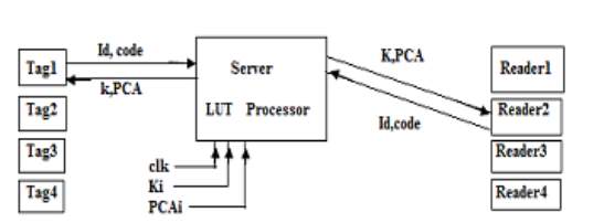
Fig 3.1. Proposed system using trusted Key Distribution Server
Figure 3.1 shows that the server maintains a LUT of tag ID and its corresponding security information. It consists of a series of keys and PCA rules combination. For experimental purpose, we have used four keys and four PCA rules. Several readers and tags come in to the scenario. Each time the key & rule combination differs and maintained by a simple clock triggered way.
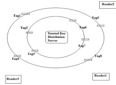
Fig 3.2. Proposed Scenario for the high security RFID system
Proposed Scenario for the high security RFID system is shown in Fig3.2. This figure shows three Reader and eight tag working at a time, where only tag1,2,3 are readable by Reader1 whereas tag4&5 are readable by Reader2 and tag6,7&8 are readable by Reader3 though all the tags are detected by all Readers, data read permission is given to specific reader only. This is very important feature of this scheme that it imposes an extra data read protection to the RFID system reducing extra memory/chip size of reader/tag. The data format of a tag will be as shown in Fig 3.3

Fig 3.3 Data format of RFID tag
Data frame of RFID tag consists of three main particulars, Tag ID, information stored by the user and the ‘Code’, which denotes the ID code for specific Reader. Either tag or reader need not remember the encryption key or PCA rule. Once data has been encrypted and stored into tag by the user, the Trusted key distribution server store as a LUT in its memory along with tag ID and ‘code’ to detect the right Reader. In a scientific research laboratory, it is very common to steal the experimental reports by other person having bad intention or may cause harm to the people. Though several techniques are which are adopted by the scientist to keep secrecy of their results, our server based security scheme will provide good performance. Some time, researcher’s contribution may be leaked through resource person to another research lab inside/outside country.
3.4 DESIGN AND IMPLEMENTATION
3.4.1 Processor for Server:
This module consists of a look-up-table incorporating a list of authentic Readers, their specific identification code, targeted tag IDs for respective Readers. Another table consists of different cellular automata rules and different Key matrices. In this work, for simplicity, we have chosen four rules with four different keys. Whenever the server receives request from a Reader, it looks in to the identification LUT and check whether the code matches with the list of authenticated Reader or not. If it is reliable, then the server acknowledges the Reader otherwise neglects the request. After receiving acknowledgement from server end, the Reader request for specific key and CA rule to decrypt the information from the tag identified by it sending the ID of the tag to the server. The server sends the information instantly to the reader.
a) Programmable Cellular Automata Rules:
Different Cellular Automata Rules are depicted in Table 1 and their rules are logical expression are listed below: The binary number (01011010)2 represents the decimal number 90 and the binary number (10010110)2 represents the decimal number 150.
TABLE 1: Programmable cellular automata rules
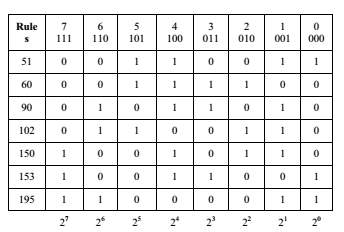
b) The PCA rules can be expressed as follows:
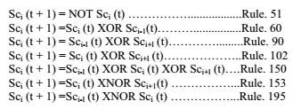
B. Tag Frame Generator:
In this proposed scheme, Tags are consists of a module named as secret code generator, which generates the code and encrypted the stored information within the tag itself. Here is an example of code generation following CA rules 90 & 150.
Secret code Generation:
Suppose we choose key Matrix as K=
Now, according to condition we have applied for this scheme, if the Ki0=’0’ then the entire row of the Key matrix will follow the rule 150 and if Ki0=’1’ then it will follow rule 90. From the chosen key Matrix, 1st, 3rd and 4th row will follow rule 90 whereas only 2nd row will follow rule 150.
For rule 90:
Data of 1st column of secret code Matrix Sc will be as Sci = Ki  Ki+1
Ki+1
Data of 4th column of secret code Matrix Sc will be as
Sci = Ki-1 Ki
Ki
Data of other column of secret code Matrix Sc will be as
Sci = Ki-1  Ki
Ki  Ki+1
Ki+1
For rule 150:
Data of 1st column of secret code Matrix Sc will be as
Sci = Ki+1
Data of 4th column of secret code Matrix Sc will be as
Sci = Ki-1
Data of other column of secret code Matrix Sc will be as
Sci = Ki-1  Ki+1
Ki+1
Following these rules,
The code Matrix for Sc will be as, Sc=
Now if this code Matrix is integrated with the tag ID, only the Reader, who knows the exact Key Matrix, will be able to decode the ID and the data or information stored within the tag. Thus prevents the data hacking by unauthorized Reader.
CHAPTER 4: HARDWARE REQUIREMENTS
4.1 GENERAL
Coordinated circuit (IC) innovation is the empowering innovation for an entire host of creative gadgets and frameworks that have changed the way we live. Jack Kil by and Robert Noyce got the 2000 Nobel Prize in Physics for their development of the incorporated circuit; without the coordinated circuit, neither transistors nor PCs would be as imperative as they are today. VLSI frameworks are substantially littler and expend less power than the discrete parts used to fabricate electronic frameworks before the 1960s.
Reconciliation permits us to manufacture frameworks with numerous more transistors, permitting substantially more registering energy to be connected to taking care of an issue. Coordinated circuits are additionally considerably less demanding to outline and make and are more solid than discrete frameworks; that makes it conceivable to create extraordinary reason frameworks that are more productive than broadly useful PCs for the main job.
4.2 APPLICATIONS OF VLSI
Electronic frameworks now play out a wide assortment of assignments in every day life. Electronic frameworks now and again have supplanted components that worked mechanically, using pressurized water, or by different means; gadgets are typically littler, more adaptable, and less demanding to benefit. In different cases electronic frameworks have made absolutely new applications. Electronic frameworks play out an assortment of undertakings, some of them unmistakable, some more covered up:
Individual excitement frameworks, for example, compact MP3 players and DVD players perform advanced calculations with strikingly little vitality.
Electronic frameworks in autos work stereo frameworks and showcases; they likewise control fuel infusion frameworks, modify suspensions to fluctuating territory, and play out the control capacities required for antilock braking (ABS) frameworks.
Computerized hardware pack and decompress video, even at top quality information rates, on-the-fly in purchaser gadgets.
Minimal effort terminals for Web perusing still require complex hardware, in spite of their committed capacity.
PCs and workstations give word-preparing, money related investigation, and recreations. PCs incorporate both focal handling units (CPUs) and extraordinary reason equipment for plate get to, quicker screen show, and so on.
Restorative electronic frameworks measure substantial capacities and perform complex handling calculations to caution about surprising conditions. The accessibility of these perplexing frameworks, a long way from overpowering purchasers, just makes interest for significantly more unpredictable frameworks. The developing modernity of uses constantly pushes the plan and assembling of incorporated circuits and electronic frameworks to new levels of intricacy.
What’s more, maybe the most stunning normal for this gathering of frameworks is its assortment as frameworks turn out to be more perplexing, we construct not a couple broadly useful PCs but rather an ever more extensive scope of uncommon reason frameworks. Our capacity to do as such is a demonstration of our developing dominance of both coordinated circuit assembling and outline, however the expanding requests of clients keep on testing the cutoff points of plan and assembling.
4.3 ADVANTAGES OF VLSI
While we will focus on incorporated circuits in this book, the properties of coordinated circuits what we can and can’t productively put in a coordinated circuit largely decide the engineering of the whole framework. Coordinated circuits enhance framework attributes in a few basic ways. ICs have three key focal points over advanced circuits worked from discrete segments:
Measure: Integrated circuits are much smaller both transistors and wires are contracted to micrometer sizes, contrasted with the millimeter or centimeter sizes of discrete parts. Little size prompts favorable circumstances in speed and power utilization, since littler segments have littler parasitic resistances, capacitances, and inductances.
Speed: Signals can be exchanged between rationale 0 and rationale 1 substantially speedier inside a chip than they can between chips. Correspondence inside a chip can happen several times quicker than correspondence between chips on a printed circuit load up.
The fast of circuits on-chip is because of their little size smaller parts and wires have littler parasitic capacitances to back off the flag.
Control utilization: Logic operations inside a chip additionally take a great deal less power. At the end of the day, bring down power utilization is to a great extent because of the little size of circuits on the chip littler parasitic capacitances and resistances require less energy to drive them.
4.4 VLSI AND SYSTEMS
These favorable circumstances of coordinated circuits convert into points of interest at the framework level:
Littler physical size: Smallness is frequently leeway in itself consider compact TVs or handheld cell phones.
Bring down power utilization: Replacing a modest bunch of standard parts with a solitary chip decreases add up to power utilization. Decreasing force utilization has a gradually expanding influence on whatever is left of the framework: a littler, less expensive power supply can be utilized; since less power utilization implies less warmth, a fan may never again be vital; a less difficult bureau with less protecting for electromagnetic protecting might be practical, as well.
Diminished cost: Reducing the quantity of parts, the power supply prerequisites, bureau expenses, et cetera, will unavoidably decrease framework cost. The gradually expanding influence of combination is with the end goal that the cost of a framework worked from custom ICs can be less, despite the fact that the individual ICs cost more than the standard parts they supplant. Understanding why incorporated circuit innovation has such significant impact on the outline of computerized frameworks requires understanding both the innovation of IC assembling and the financial matters of ICs and advanced frameworks.
4.5 INTEGRATED CIRCUIT MANUFACTURING
Coordinated circuit innovation depends on our capacity to make colossal quantities of little devices today, more transistors are fabricated in California every year than raindrops fall on the state. In this area, we quickly overview VLSI fabricating.
Innovation
Most assembling procedures are decently firmly coupled to the thing they are assembling. A sequential construction system worked to deliver Buicks, for instance, would need to experience direct revamping to fabricate Chevys tools like sheet metal molds would need to be supplanted, and even a few machines would need to be adjusted. Also, either mechanical production system would be far expelled from what is required to create electric drills.
4.6 MASK-DRIVEN MANUFACTURING
- Coordinated circuit fabricating innovation, then again, is astoundingly flexible. While there are a few assembling forms for various circuit types CMOS, bipolar, etc. a fabricating line can make any circuit of that sort basically by changing a couple of essential devices called veils. For instance, a solitary CMOS fabricating plant can make both microchips and microwave stove controllers by changing the veils that shape the examples of wires and transistors on the chips.
- Silicon wafers are the crude material of IC assembling. The manufacture procedure frames designs on the wafer that make wires and transistors. a progression of indistinguishable chips are designed onto the wafer (with some space saved for test circuit structures which permit assembling to gauge the consequences of the assembling procedure).
- The IC fabricating procedure is effective in light of the fact that we can create numerous indistinguishable chips by handling a solitary wafer. By changing the covers that figure out what examples are set down on the chip, we decide the advanced circuit that will be made.
- The IC creation line is a non specific assembling line we can rapidly retool the line to make extensive amounts of another sort of chip, utilizing a similar handling steps utilized for the linear past item.
4.7 CIRCUITS AND LAYOUTS
- We could assemble a breadboard circuit out of standard parts. To manufacture it on an IC creation line, we should go above and beyond and plan the design, or examples on the veils. The rectangular shapes in the design (appeared here as an outline called a stick chart) frame transistors and wires which fit in with the circuit in the schematic.
- Making formats is extremely tedious and exceptionally important the size of the design decides the cost to produce the circuit, and the states of components in the design decide the speed of the circuit also. Amid assembling, a photolithographic (photographic printing) process is utilized to exchange the design designs from the veils to the wafer. The examples left by the veil are utilized to specifically change the wafer: contaminations are included at chosen areas in the wafer; protecting and leading materials are included top of the wafer also.
- These creation steps require high temperatures, little measures of exceedingly lethal chemicals, and amazingly clean conditions. Toward the finish of preparing, the wafer is isolated into various chips.
4.8 MANUFACTURING DEFECTS
- Since no assembling procedure is flawless, a portion of the chips on the wafer may not work. Since no less than one deformity is certain to happen on every wafer, wafers are cut into littler, working chips; the biggest chip that can be sensibly fabricated today is 1.5 to 2 cm on a side, while a wafer is in moving from 30 to 45 cm. Each chip is independently tried; the ones that breeze through the test are spared after the wafer is diced into chips. The working chips are set in the bundles recognizable to advanced creators.
- In a few bundles, little wires associate the chip to the packages pins while the bundle body shields the chip from taking care of and the components; in others, patch knocks straightforwardly interface the chip to the bundle. Incorporated circuit assembling is a capable innovation for two reasons: all circuits can be made out of a couple sorts of transistors and wires; and any mix of wires and transistors can be based on a solitary manufacture line just by changing the veils that decide the example of segments on the chip. Coordinated circuits run quick on the grounds that the circuits are little.
- Similarly as vital, we are not stuck building a couple of standard chip types we can fabricate any capacity we need. The adaptability given by IC producing gives we a chance to assemble quicker, more intricate advanced frameworks in ever more prominent assortment.
4.9 ECONOMICS
Since incorporated circuit fabricating has so much leverage incredible number of parts a be worked with a couple of standard assembling procedures extraordinary arrangement of exertion has gone into enhancing IC producing. Be that as it may, as chips turn out to be more perplexing, the cost of planning a chip goes up and turns into a noteworthy piece of the general cost of the chip.
Moore Law
In the 1960s Gordon Moore anticipated that the quantity of transistors that could be made on a chip would develop exponentially. His expectation, now known as Moores Law, was strikingly farsighted. Moore extreme forecast was that transistor check would twofold like clockwork, a gauge that has held up astoundingly well. Today, an industry bunch keeps up the International Technology Roadmap for Semiconductors (ITRS), that maps out systems to keep up the pace of Moore Law.
Phrasing
The most fundamental parameter related with an assembling procedure is the base channel length of a transistor. (In this book, for instance, we will use for instance an innovation that can fabricate 180 nm transistors.) An assembling innovation at a specific channel length is known as an innovation hub. We regularly allude to a group of innovations at comparative component sizes: micron, submicron, profound submicron, and now nanometer advancements. The term nanometer innovation is by and large utilized for advancements underneath 100 nm.
4.10 COST OF MANUFACTURING
- IC producing plants are greatly costly. A solitary plant costs as much as $4 billion. Given that another, best in class fabricating procedure is produced like clockwork, that is a sizeable venture. The venture bodes well on the grounds that a solitary plant can produce such a variety of chips and can without much of a stretch be changed to fabricate distinctive sorts of chips.
- In the early years of the incorporated circuits business, organizations concentrated on building vast amounts of a couple of standard parts. These parts are commodities one 80 ns, 256Mb element RAM is pretty much the same as whatever other, paying little heed to the maker.
- Organizations focused on item parts to some degree since assembling procedures were less surely knew and producing varieties are less demanding to monitor when a similar part is being manufactured for quite a while.
- Standard parts additionally seemed well and good since outlining incorporated circuits was hard not just the circuit, however the format must be planned, and there were few PC projects to help mechanize the plan procedure.
4.11 COST OF DESIGN
- One of the less blessed outcomes of Moore Law is that the time and cash required to plan a chip goes up consistently. The cost of planning a chip originates from a few elements:
- Gifted originators are required to determine, planner, and execute the chip. A plan group may run from about six individuals for a little chip to 500 individuals for an expansive, superior microchip
- These originators can’t work without access to an extensive variety of PC helped outline (CAD) devices. These apparatuses incorporate rationale, make formats, reproduce, and confirm outlines. Computer aided design apparatuses are for the most part authorized and you should pay a yearly expense to keep up the permit. A permit for a solitary duplicate of one instrument, for example, rationale combination, may cost as much as $50,000 US.
- The CAD instruments require an extensive register cultivate on which to run. Amid the most serious piece of the outline procedure, the plan group will keep many PCs running persistently for quite a long time or months.
- An expansive ASIC, which contains a great many transistors however is not manufactured on the cutting edge process, can without much of a stretch cost $20 million US and as much as $100 million. Outlining an extensive chip costs a huge number of dollars.
Configuration COSTS AND IP
We can spread these plan costs over more chips in the event that we can reuse all or some portion of the outline in different chips. The high cost of configuration is the essential inspiration for the ascent of IP-based outline, which makes modules that can be reused in a wide range of plans
4.12 TYPES OF CHIPS
- The dominance of standard parts pushed the issues of building modified frameworks back to the board-level fashioners who utilized the standard parts.
- Since a capacity worked from standard parts generally requires a bigger number of segments than if the capacity were worked with specially crafted ICs, planners tended to assemble littler, less complex frameworks. The modern pattern, be that as it may, is to make accessible a more extensive assortment of incorporated circuits. The more prominent assorted qualities of chips incorporates:
More specific standard parts:
- In the 1960s, standard parts were rationale entryways; in the 1970s they were LSI segments. Today, standard parts incorporate genuinely particular segments: correspondence organize interfaces, representation quickening agents, skimming point processors. Every one of these parts are more specific than microchips however are utilized as a part of enough volume that outlining uncommon reason chips is justified regardless of the exertion.
- Truth be told, putting an intricate, superior capacity on a solitary chip regularly makes different applications possible for case, single-chip drifting point processors make fast numeric calculation accessible on even cheap PCs.
Application-particular incorporated circuits (ASICs)
Instead of construct a framework out of standard parts, architects can now make a solitary chip for their specific application. Since the chip is specific, the elements of a few standard parts can frequently be pressed into a solitary chip, lessening framework estimate, power, warmth, and cost. Application-particular ICs are conceivable in view of PC instruments that help people configuration chips substantially more rapidly.
Systems-on-chips (SoCs).
- Manufacture innovation has progressed to the point that we can put a total framework on a solitary chip. For instance, a solitary chip PC can incorporate a CPU, transport, I/O gadgets, and memory. SoCs permit frameworks to be made at much lower cost than the identical board-level framework. SoCs can likewise be higher execution and lower control than board-level counterparts in light of the fact that on-chip associations are more productive than chip-to chip associations.
- A more extensive assortment of chips is presently accessible to a limited extent since manufacture techniques are better comprehended and more solid. All the more vitally, as the quantity of transistors per chip develops, it winds up plainly less demanding and less expensive to plan unique reason ICs. At the point when just a couple of transistors could be put on a chip, cautious plan was required to guarantee that even unobtrusive capacities could be put on a solitary chip. Today VLSI fabricating forms, which can put a large number of painstakingly outlined transistors on a chip, can likewise be utilized to put countless less-precisely planned transistors on a chip.
- Despite the fact that the chip could be made littler or speedier with more plan exertion, the benefits of having a solitary chip usage of a capacity that can be immediately planned frequently exceed the lost potential execution.
- The issue and the test of the capacity to produce such substantial chips is design the capacity to make successful utilization of the a huge number of transistors on a chip to play out a helpful capacity.
4.13 CMOS TECHNOLOGY
CMOS is the predominant coordinated circuit innovation. In this segment we will present some essential ideas of CMOS to comprehend why it is so boundless and a portion of the difficulties presented by the inborn qualities of CMOS.
4.13.1 POWER CONSUMPTION
CONTROL CONSUMPTION CONSTRAINTS:
- The tremendous chips that can be manufactured today are conceivable simply because of the generally minor utilization of CMOS circuits. Control utilization is basic at the chip level since a great part of the power is scattered as warmth, and chips have restricted warmth dissemination limit. Regardless of the possibility that the framework in which a chip is put can supply a lot of energy, most chips are bundled to disperse less than 10 to 15 Watts of energy before they endure perpetual harm (however a few chips scatter well more than 50 Watts on account of extraordinary bundling).
- The power utilization of a rationale circuit can, in the most pessimistic scenario, confine the number transistors we can adequately put on a solitary chip. Restricting the quantity of transistors per chip changes framework plan in a few ways. Most clearly, it expands the physical size of a framework. Utilizing powerful circuits additionally expands control supply and cooling necessities.
- A more unobtrusive impact is brought about by the way that the time required to transmit a flag between chips is substantially bigger than the time required to send a similar flag between two transistors on a similar chip; accordingly, a portion of the upside of utilizing a higher-speed circuit family is lost. Another inconspicuous impact of diminishing the level of joining is that the electrical plan of multi-chip frameworks is more mind boggling: minuscule wires on-chip display parasitic resistance and capacitance, while perceptible wires between chips have capacitance and inductance, which can bring about various ringing impacts that are considerably harder to investigate.
- The cozy connection between power utilization and warmth makeslow-control outline procedures imperative information for each CMOS originator. Obviously, low-vitality configuration is particularly vital in battery-worked frameworks like cell phones. Vitality, interestingly, must be spared by maintaining a strategic distance from superfluous work.
- We will see all through whatever is left of this book limiting force and vitality utilization requires cautious meticulousness at each level of reflection, from framework engineering down to design.
- As CMOS elements wind up noticeably littler, extra power utilization instruments become possibly the most important factor. Customary CMOS devours control when signs change however expends just immaterial power when sit out of gear. In present day CMOS, spillage components begin to deplete current
4.13.2 DESIGN AND TESTABILITY
Outline VERIFICATION
- Our capacity to assemble substantial chips of boundless assortment presents the issue of checking whether those chips have been made accurately. Originators acknowledge the need to check or approve their outlines to ensure that the circuits play out the predefined work. (A few people utilize the terms confirmation and approval conversely; a better qualification saves check for formal evidences of rightness, leaving approval to mean any method which builds trust in accuracy, for example, recreation.)
- Chip outlines are mimicked to guarantee that the chips circuits figure the best possible capacities to a succession of sources of info practiced the chip. Fabricating test however each chip that falls off the assembling line should likewise experience
Fabricating test:
- The chip must be practiced to show that no assembling abandons rendered the chip futile. Since IC fabricating has a tendency to present certain sorts of deformities and in light of the fact that we need to limit the time required to test each chip, we can simply utilize the info successions made for plan check to perform producing test. Each chip must be intended to be completely and effortlessly testable. Discovering that a chip is terrible simply after you have connected it to a framework is irritating, best case scenario and unsafe even under the least favorable conditions. Clients are probably not going to continue utilizing makers who frequently supply awful chips.
- Absconds presented amid assembling range from the catastrophic sullying that devastates each transistor on the wafer to the subtle a single broken wire or a crystalline deformity that slaughters just a single transistor. While some awful chips can be discovered effectively, each chip must be altogether tried to discover even inconspicuous defects that deliver incorrect outcomes just every so often. Tests intended to exercise usefulness and uncover configuration bugs don’t dependably reveal fabricating deserts. We utilize blame models to recognize potential assembling issues and decide how they influence the chips operation.
- The most well-known blame model is trapped at-0/1: the imperfection causes a rationale gates yield to be dependably 0 (or 1), autonomous of the gates input values. We can frequently decide if a rationale gates yield is stuck regardless of the possibility that we cant specifically watch its yields or control its data sources. We can produce a decent arrangement of assembling tests for the chip by accepting every rationale gates yield is stuck at 0 (then 1) and finding a contribution to the chip which causes diverse yields when the blame is available or truant.
4.13.3 TESTABILITY AS A DESIGN PROCESS
- Shockingly, not all chip outlines are similarly testable. A few issues may require long info arrangements to uncover; different shortcomings may not be testable by any means, despite the fact that they cause chip glitches that aren’t secured by the blame model. Generally, chip architects have overlooked testability issues, abandoning them to a different test build who must locate an arrangement of contributions to sufficiently test the chip. In the event that the test build can’t change the chip configuration to settle testability issues, his or her employment winds up plainly both troublesome and offensive. The outcome is regularly inadequately tried chips whose assembling issues are discovered simply after the client has connected them to a framework.
- Organizations now perceive that the best way to convey top notch chips to clients is to make the chip planner in charge of testing, similarly as the architect is in charge of making the chip keep running at the required speed. Testability issues can frequently be settled effectively ahead of schedule in the plan procedure at moderately little cost in territory and execution. In any case, current fashioners must comprehend testability prerequisites, investigation systems which recognize hard-to-test segments of the plan, and outline methods which enhance testability
4.13.4 RELIABILITY
Unwavering quality IS A LIFETIME PROBLEM
- Prior eras of VLSI innovation were sufficiently powerful that testing chips at assembling time was adequate to distinguish working parts a chip either worked or it did not. In today’s nanometer-scale advances, the issue of deciding if a chip works is more mind boggling. Various systems can bring about transient disappointments that cause periodic issues yet are not repeatable. Some other disappointment instruments, such as overheating, cause lasting disappointments yet simply after the chip have worked for quite a while. Also, more perplexing assembling issues cause issues that are harder to analyze and may influence execution instead of usefulness.
4.13.5 DESIGN-FOR MANUFACTURABILITY
- Various methods, alluded to as plan for-manufacturability or outline for-yield, are being used today to enhance the dependability of chips that fall off the assembling line. We can make chips more dependable by outlining circuits and models that lessen configuration stresses and check for issues. For instance, warmth is one noteworthy reason for chip disappointment. Appropriate power administration hardware can decrease the chip warm dispersal and diminish the harm brought on by overheating. We likewise need to change the way we configuration chips.
- A portion of the helpful levels of deliberation that served us well in before advancements are no longer completely proper in nanometer innovations. We have to check all the more altogether and take care of unwavering quality issues by changing plan choices made before.
4.13.6 INTEGRATED CIRCUIT DESIGN TECHNIQUES
To make utilization of the surge of transistors given to us by Moore Law, we should outline vast, complex chips rapidly. The impediment to making huge chips work effectively is complexity many intriguing thoughts for chips have kicked the bucket in the marsh of points of interest that must be made right before the chip really works. Coordinated circuit configuration is hard in light of the fact that originators must juggle a few unique issues:
Multiple levels of reflection:
IC configuration requires refining a thought through many levels of detail. Beginning from a determination of what the chip must do, the planner must make an engineering which plays out the required capacity, extend the design into a rationale outline, and further grow the rationale outline into a format like the one in Figure 1-2. As you will learn before the finish of this book, the determination to-format configuration process is a great deal of work.
Multiple and clashing expenses:
Notwithstanding drawing a plan through many levels of detail, the originator should likewise consider costs not dollar costs, yet criteria by which the nature of the outline is judged. One basic cost is the speed at which the chip runs. Two designs that execute a similar capacity (increase, for instance) may keep running at altogether different velocities. We will see that chip zone is another basic outline cost: The cost of assembling a chip is exponentially identified with its zone, and chips considerably bigger than 1 cm2 can’t be fabricated by any means. Moreover, if different cost criteria such as territory and speed requirements must be fulfilled, many plan choices will enhance one cost metric to the detriment of the other. Configuration is commanded by the way toward adjusting clashing imperatives.
Short plan time:
In a perfect world, a creator would have sufficient energy to think about the impact of a plan choice. We don’t, be that as it may, live in a perfect world. Chips which show up past the point of no return may profit since contenders have grabbed piece of the overall industry. Along these lines, fashioners are under weight to configuration chips as fast as could be expected under the circumstances. Configuration time is particularly tight in application-particular IC outline, where just half a month might be accessible to transform an idea into a working ASIC.
4.14 FIELD-PROGRAMMABLE GATE ARRAYS (FPGA)
- A field-programmable door exhibit (FPGA) is a square of programmable rationale that can execute multi-level rationale capacities. FPGAs are most ordinarily utilized as partitioned product chips that can be customized to execute vast capacities.
- Be that as it may, little squares of FPGA rationale can be helpful segments on-chip to permit the client of the chip to redo some portion of the chip coherent capacity. A FPGA piece must execute both combinational rationale capacities and interconnect to have the capacity to develop multi-level rationale capacities. There are a few unique innovations for programming FPGAs, yet most rationale procedures are probably not going to execute hostile to wires or comparable hard programming advances, so we will focus on SRAM-customized FPGAs.
4.14.1 LOOKUP TABLES
- The essential technique used to fabricate a combinational rationale piece (CLB) additionally called a rationale element in a SRAM-based FPGA is the query table (LUT). As appeared in Figure , the query table is a SRAM that is utilized to actualize a truth table.
- Each address in the SRAM speaks to a mix of contributions to the rationale component. The esteem put away at that address speaks to the estimation of the capacity for that information Combination an info work requires a SRAM with area.
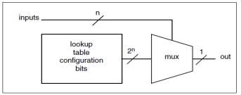
Figure 4.1 Lookup Tables
Since an essential SRAM is not timed, the query table rationale component works much as whatever other rationale entryway as its data sources changes, its yield changes after some postponement. Each address in the SRAM speaks to a mix of contributions to the rationale component. The esteem put away at that address speaks to the estimation of the capacity for that info Combination an information work requires a SRAM with area.
4.14.2 PROGRAMMING A LOOKUP TABLE
Not at all like a run of the mill rationale door, the capacity spoke to by the rationale component can be changed by changing the estimations of the bits put away in the SRAM. Subsequently, the n-input rationale component can speak to capacities (however some of these capacities are stages of each other).

Figure 4.2 Programming A Lookup Table
A commonplace rationale component has four data sources. The postponement through the query table is autonomous of the bits put away in the SRAM, so the deferral through the rationale component is the same for all capacities. This implies, for instance, a query table-based rationale component will display a similar postponement for a 4-input XOR and a 4-input NAND.
Interestingly, a 4-input XOR worked with static CMOS rationale is significantly slower than a 4-input NAND. Obviously, the static rationale door is by and large quicker than the rationale component. Rationale components by and large contain registers flip-flops and latches as well as combinational rationale.
A flip-flounder or hook is little contrasted with the combinational rationale component (in sharp difference to the circumstance in custom VLSI), so it bodes well to add it to the combinational rationale component. Utilizing a different cell for the memory component would just take up directing assets. The memory component is associated with the yield; regardless of whether it stores a given esteem is controlled by its clock and empower inputs.
4.14.3 COMPLEX LOGIC ELEMENT
Numerous FPGAs likewise consolidate particular viper rationale in the rationale component. The basic part of a viper is the convey chain, which can be actualized.
Substantially more productively in specific rationale than it can utilizing standard query table strategies. The wiring channels that associate with the rationale elements sources of info and yields additionally should be programmable. A wiring channel has various programmable associations with the end goal that each information or yield by and large can be associated with any of a few distinct wires in the channel.
4.14.4 PROGRAMMABLE INTERCONNECTION POINTS
Straightforward variant of an interconnection point, regularly known as an association box.

Figure 4.3 Programming A Lookup Table
- A programmable association between two wires is made by a CMOS transistor (a pass transistor). The pass transistors entryway is controlled by a static memory program bit (appeared here as a D register).When the pass transistors door is high, the transistor leads and interfaces the two wires; when the door is low, the transistor is off and the two wires are not associated.
- A flip-tumble or lock is little contrasted with the combinational rationale component (in sharp differentiation to the circumstance in custom VLSI), so it bodes well to add it to the combinational rationale component. Utilizing a different cell for the memory component would essentially take up steering assets. The memory component is associated with the yield; regardless of whether it stores a given esteem is controlled by its clock and empower inputs.
- The wiring channels that interface with the rationale elements data sources and yields additionally should be programmable. A wiring channel has various programmable associations with the end goal that each information or yield for the most part can be associated with any of a few distinct wires in the channel.
CHAPTER 5: Apparatuses
5.1 Introduction
The primary instruments required for this venture can be ordered into two general classifications.
Equipment necessity
Programming necessity
5.2 Equipment Requirements
FPGA Kit
In the equipment section a typical PC where Xilinx ISE 10.1i programming can be effortlessly worked is required, i.e., with a base framework arrangement Pentium III, 1 GB RAM, 20 GB Hard Disk.
5.3 Software Requirements
MODELSIM 6.4b
XILINX 10.1
It requires Xilinx ISE 10.1 adaptation of programming where Verilog source code can be utilized for plan execution.
Prologue To Model sim:
In Model sim, all outlines are gathered into a library. You normally begin another reproduction in Model Sim by making a working library called “work”. “Work” is the library name utilized by the compiler as the default goal for accumulated outline units.
Ordering Your Design: After making the working library, you gather your plan units into it. The Model Sim library arrangement is perfect over every single bolstered stage. You can reenact your plan on any stage without having to recompile your outline.
Stacking the Simulator with Your Design and Running the Simulation With the outline gathered, you stack the test system with your plan by summoning the test system on a top-level module (Verilog) or a setup or substance/engineering pair (VHDL). Accepting the plan stacks effectively, the reproduction time is set to zero, and you enter a run charge to start reenactment.
Troubleshooting your outcomes in the event that you don’t get the outcomes you expect, you can utilize Model Sims powerful investigating condition to find the reason for the issue.
Models Supported:
Model Sim VHDL bolsters both the IEEE 1076-1987 and 1076-1993 VHDL, the 1164-1993 Standard Multi value Logic System for VHDL Interoperability, and the 1076.2-1996 Standard VHDL Mathematical Packages measures. Any plan created with Model Sim will be good with whatever other VHDL framework that is consistent with either IEEE Standard 1076-1987 or 1076-1993. Model Sim Verilog depends on IEEE Std 1364-1995 and a fractional usage of 1364-2001, Standard Hardware Description Language Based on the Verilog Hardware Description Language. The Open Verilog International Verilog LRM rendition 2.0 is likewise appropriate to a huge degree. Both PLI (Programming Language Interface) and VCD (Value Change Dump) are bolstered for ModelSim PE and SE clients.
5.4 MODELSIM
Essential Steps for Simulation
This segment gives additionally detail identified with each progression during the time spent reproducing your outline utilizing ModelSim.
Step 1 – Collecting Files and Mapping Libraries
Records expected to run Model Sim on your outline:
configuration records (VHDL, Verilog, or potentially System C), including boost for the plan libraries, both working and asset
modelsim.ini (consequently made by the library mapping charge)
Giving jolt to the outline
You can give jolt to your outline in a few ways:
Dialect based test seat
Tcl-based ModelSim intelligent summon, constrain
VCD records/charges
See “Utilizing developed VCD as jolt” (UM-458) and “Utilizing broadened VCD as boost”
outsider test seat era apparatuses
What is a library in ModelSim?
A library is an area where information to be utilized for reenactment is put away. Libraries are Model Sims method for dealing with the production of information before it is required for use in reproduction. It likewise fills in as an approach to streamline reenactment summon. Rather than accumulating all plan information every last time you recreate, Model Sim utilizes paired pre-incorporated information from these libraries. Along these lines, on the off chance that you roll out improvements to a solitary Verilog module, just that module is recompiled, as opposed to all modules in the outline.
Working and asset libraries
Outline libraries can be utilized as a part of two routes: 1) as a nearby working library that contains the assembled rendition of your plan; 2) as an asset library. The substance of your working library will change as you refresh your outline and recompile. An asset library is normally perpetual, and fills in as a sections hotspot for your plan. Cases of asset libraries may be: shared data inside your gathering, merchant libraries, bundles, or already accumulated components of your own working plan.
You can make your own asset libraries, or they might be provided by another plan group or an outsider (e.g., a silicon seller). For more data on asset libraries and working libraries, see “Working library versus asset libraries”, “Overseeing library substance”, “Working with outline libraries, and “Indicating the asset librarie”.
Making the Logical Library vlib
Before you can incorporate your source records, you should make a library in which to store the gathering comes about. You can make the legitimate library utilizing the GUI, utilizing File > New > Library (see “Making a library”), or you can utilize the vlib summon. For instance, the summon:
vlib work makes a library named work. As a matter of course, gathering results are put away in the work library
Mapping The Logical Work To The Physical Work Directory vmap
VHDL utilizes consistent library names that can be mapped to Model Sim library catalogs. On the off chance that libraries are not mapped legitimately, and you summon your reproduction, fundamental segments won’t be stacked and reenactment will come up short. Correspondingly, assemblage can likewise rely on upon legitimate library mapping.
As a matter of course, Model Sim can discover libraries in your present catalog (expecting they have the correct name), however for it to discover libraries found somewhere else, you have to delineate sensible library name to the pathname of the library. You can utilize the GUI (“Library mappings with the GUI”, an order (“Library mappings with the GUI” ), or a venture (“Getting started with tasks” to allot an intelligent name to an outline library.
The configuration for summon line passage is:
vmap
This summon sets the mapping between a legitimate library name and a registry.
Step 2 – Compiling the outline with vlog/vcom/sccom
Plans are accumulated with one of the three dialect compilers.
Aggregating Verilog – vlog
Model Sim compiler for the Verilog modules in your plan is vlog . Verilog documents might be arranged in any request, as they are not arrange subordinate. See “Gathering Verilog documents” for details.Verilog parts of the outline can be enhanced for better reproduction execution.
“Improving Verilog outlines”.
Incorporating VHDL vcom
ModelSim compiler for VHDL plan units is vcom . VHDL records must be incorporated by the outline necessities of the plan. Ventures may help you in deciding the incorporate request: for more data, see”Auto-creating assemble arrange” (UM-46). See “Aggregating VHDL records” (UM-73) for subtle elements. on VHDL gathering.
Accumulating System com
ModelSim compiler for SystemC outline units is sccom , and is utilized just in the event that you have System C segments in your plan. See “Assembling System C records” for subtle elements.
Step 3 – Loading the outline for reproduction
vsim
Your plan is prepared for reenactment after it has been ordered and (alternatively) upgraded with vopt . For more data on improvement, see Optimizing Verilog outlines. You may then conjure vsim with the names of the top-level modules (many outlines contain just a single top-level module) or the name you appointed to the streamlined rendition of the plan.
For instance, if your top-level modules are “testbench” and “globals”, then summon the test system as takes after:
vsim testbench globals
After the test system stacks the top-level modules, it iteratively loads the instantiated modules and UDPs in the plan chain of importance, connecting the outline together by interfacing the ports and settling various leveled references.
Utilizing SDF
You can fuse real postpone qualities to the recreation by applying SDF back explanation documents to the outline. For more data on how SDF is utilized as a part of the plan, see “Indicating SDF documents for reenactment” .
Step 4 – Simulating the plan
Once the plan has been effectively stacked, the recreation time is set to zero, and you should enter a run charge to start reproduction. For more data, see Verilog reproduction, VHDL recreation , and System reenactment .
The essential test system charges are: include
wave
force
bp
run
step
next
Step 5- Debugging The Design
Numerous tools and windows useful in debugging your design are available from the Model Sim GUI. For more information, see Waveform analysis (UM-237), PSL Assertions and Tracing signals with the Dataflow window. In addition, several basic simulation commands are available from the command line to assist you in debugging your design: d
escribe
drivers
examine
force
log
checkpoint
restore
show
A programmable connection between two wires is made by a CMOS transistor (a pass transistor). The pass transistors gate is controlled by a static memory program bit (shown here as a D register).When the pass transistors gate is high, the transistor conducts and connects the two wires; when the gate is low, the transistor is off and the two wires are not connected.
A flip-flop or latch is small compared to the combinational logic element (in sharp contrast to the situation in custom VLSI), so it makes sense to add it to the combinational logic element. Using a separate cell for the memory element would simply take up routing resources. The memory element is connected to the output; whether it stores a given value is controlled by its clock and enable inputs.
The wiring channels that connect to the logic elements inputs and outputs also need to be programmable. A wiring channel has a number of programmable connections such that each input or output generally can be connected to any one of several different wires in the channel. On the left side of the interface, under the project tab is the frame listing of the files that pertainto the opened project. The Library frame lists the entities of the project (that have been ompiled).To the right is the Model Sim shell frame. It is an extension of MS-DOS, so both Model Sim and MS-DOS commands can be executed
Numerous tools and windows useful in debugging your design are available from the ModelSim GUI. For more information, see Waveform analysis (UM-237), PSL Assertions and Tracing signals with the Dataflow window. In addition, several basic simulation commands are available from the command line to assist you in debugging your design:
You can incorporate actual delay values to the simulation by applying SDF back annotation files to the design. For more information on how SDF is used in the design, see “Specifying SDF files for simulation unchanging, and serves as a parts source for your design. Examples of resource libraries might be shared information within your group, vendor libraries, packages, or previously compiled elements of your own working design.
You can create your own resource libraries, or they may be supplied by another design team or a third party (e.g., a silicon vendor). For more information on resource libraries and working libraries, see “Working library versus resource libraries”, “Managing library contents”, “Working with design libraries, and “Specifying the resource library.
5.5 MODELSIM BASICS
On the left side of the interface, under the project tab is the frame listing of the files that pertain to the opened project. The Library frame lists the entities of the project (that have been ompiled).To the right is the ModelSim shell frame. It is an extension of MS-DOS, so both ModelSim and MS-DOS commands can be executed.
A. Creating a New Project
Once ModelSim has been started, create a new project:
File > New > Project¦
Name the project FA, set the project location
to F:/VHDL , and click OK.
A new window should appear to add new files to the project. Choose Create New File.

Enter F:VHDLFA.vhd as the file name and click OK.
Then close the add new files window.
Additional files can be added later by choosing from the menu: Project > Add File to Project
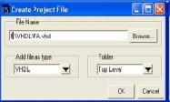
B. Editing Source Files
Double click the FA.vhd source found under the Workspace windows project tab. This will open up an empty text editor configured to highlight VHDL syntax. Copy the source found at the end of this document. After writing the code for the entity and its architecture, save and close the source file
C. Arranging ventures
Select the record from the venture documents list edge and right tap on it. Select gather to simply aggregate. This records or arrange just for the documents in the present venture. On the off chance that there are mistakes inside the code or the venture, a red disappointment message will be shown. Double tap these red blunders for more definite mistakes. Something else, if all is well then no red cautioning or mistake messages will be shown. Another window will be shown posting the plan entity signals and their underlying quality (demonstrated as follows). Things in waveform and posting are requested in a similar request in which they are pronounced in the code.
To show the waveform, select the signs for the waveform to show (hold CTL and snap to choose numerous signs) and from the flag list window menu select. For this situation, it is conceivable to utilize Verilog to compose a test seat to check the usefulness of the plan utilizing documents on the host PC to characterize jolts, to interface with the client, and to contrast comes about and those normal.
A Verilog model is converted into the “doors and wires” that are mapped onto a programmable rationale gadget, for example, a CPLD or FPGA, and then it is the real equipment being arranged, as opposed to the Verilog code being “executed” as though on some type of a processor chip. For this situation, it is conceivable to utilize Verilog to compose a test seat to confirm the usefulness of the plan utilizing documents on the host PC to characterize boosts, to communicate with the client, and to contrast comes about and those normal. FPGA remains for Field Programmable Gate Array which has the variety of rationale module, I/O module and directing tracks (programmable interconnect). FPGA can be designed by end client to execute particular hardware. Speed is up to 100 MHz yet at present speed is in GHz.
Fundamental applications are DSP, FPGA based PCs, rationale copying, ASIC and ASSP. FPGA can be modified essentially on SRAM (Static Random Access Memory). It is Volatile and primary preferred standpoint of utilizing SRAM programming innovation is re-configurability. Issues in FPGA innovation are multifaceted nature of rationale component, clock bolster, IO support and interconnections (Routing).
II. Mimicking with ModelSim
To mimic, first the element configuration must be stacked into the test system. Do this by choosing from the menu:
Reproduce > Simulate
Another window will show up posting every one of the elements (not filenames) that are in the work library. Select FA substance for reenactment and snap OK.
Intermittently it will be important to make substances with numerous models. For this situation the engineering must be indicated for the reproduction. Extend the tree for the element and select the engineering to be recreated and after that snap OK.
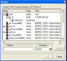
Often times it will be necessary to create entities with multiple architectures. In this case the architecture has to be specified for the simulation. Expand the tree for the entity and select the architecture to be simulated and then click OK. Making test records for the test system after the plan is stacked, clear up any past information and restarts the clock by writing in the Prompt:
See > Signals
Another window will be shown posting the outline entities signals and their underlying worth (demonstrated as follows). Things in waveform and posting are requested in a similar request in which they are announced in the code. To show the waveform, select the signs for the waveform to show (hold CTL and snap to choose various signs) and from the flag list window menu select:
Include > Wave > Selected signs
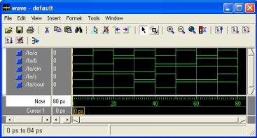
Essential Simulation Flow:
The accompanying chart demonstrates the fundamental strides for mimicking an outline in ModelSim.
Create a working library

Compile design files

Debug results

Load and Run
Simulation
Figure. 5.1 Basic recreation stream
Extend configuration stream:
- As should be obvious, the stream is like the fundamental reproduction stream. Notwithstanding, there are two imperative contrasts:
- You don’t need to make a working library in the venture stream; it is accomplished for you Consequently.
- Tasks are industrious. As it were, they will open each time you conjure Modelsim unless you particularly close them.
The accompanying outline demonstrates the fundamental strides for recreating a plan inside a Modelsim extend.
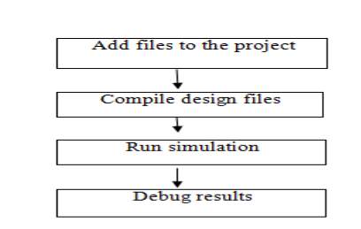
Figure: 5.2 Design Project F low
5.6 Prologue To XILINX ISE
This apparatus can be utilized to make, execute, mimic, and integrate Verilog outlines for usage on FPGA chips.
- ISE: Integrated Software Environment
- Condition for the advancement and trial of computerized frameworks configuration focused to FPGA or CPLD
- Incorporated accumulation of instruments available through a GUI
- In light of a coherent union motor (XST: Xilinx Synthesis Technology)
- XST underpins distinctive dialects:
- Verilog
- VHDL
- XST deliver a net rundown coordinated with requirements
- Underpins every one of the means required to finish the plan:
- Decipher, guide, place and course
- Bit stream era
For this situation, it is conceivable to utilize Verilog to compose a test seat to check the usefulness of the plan utilizing documents on the host PC to characterize jolts, to cooperate with the client, and to contrast comes about and those normal.
- A Verilog model is converted into the “entryways and wires” that are mapped onto a programmable rationale gadget, for example, a CPLD or FPGA, and then it is the genuine equipment being arranged, instead of the Verilog code being “executed” as though on some type of a processor chip.
- Execution:
- Amalgamation (XST)
- Create a netlist record beginning from a HDL portrayal
- Decipher (NGDBuild)
- Changes over all information outline netlists and afterward composes the outcomes into a solitary combined record, that depicts rationale and requirements.
- Mapping (MAP)
- Maps the rationale on gadget parts.
- Takes a netlist and gatherings the intelligent components into CLBs and IOBs (parts of FPGA).
- Place And Route (PAR)
- Put FPGA cells and interfaces cells.
- Bit stream era
- XILINX Design Process
Step 1: Design section
- HDL (Verilog or VHDL, ABEL x CPLD), Schematic Drawings, Bubble Diagram
Step 2: Synthesis
- Translates .v, .vhd, .sch documents into a netilist record (.ngc)
Step 3: Implementation
- FPGA: Translate/Map/Place and Route, CPLD: Fitter
Step 4: Configuration/Programming
- Download a BIT document into the FPGA
- Program JEDEC document into CPLD
- Program MCS document into Flash PROM
- Recreation can happen after strides 1, 2, 3
5.7 Introduction to FPGA
FPGA remains for Field Programmable Gate Array which has the variety of rationale module, I/O module and directing tracks (programmable interconnect). FPGA can be designed by end client to actualize particular hardware. Speed is up to 100 MHz however at present speed is in GHz.
Principle applications are DSP, FPGA based PCs, rationale imitating, ASIC and ASSP. FPGA can be modified essentially on SRAM (Static Random Access Memory). It is Volatile and primary favorable position of utilizing SRAM programming innovation is re-configurability. Issues in FPGA innovation are many-sided quality of rationale component, clock bolster, IO support and interconnections (Routing).
FPGA Design Flow
FPGA contains a two dimensional varieties of rationale squares and interconnections between rationale pieces. Both the rationale pieces and interconnects are programmable. Rationale pieces are modified to actualize a coveted capacity and the interconnects are customized utilizing the change boxes to interface the rationale squares.
To be all the more clear, on the off chance that we need to execute a mind boggling outline (CPU for example), then the plan is separated into little sub capacities and each sub capacity is actualized utilizing one rationale square. Presently, to get our coveted outline (CPU), all the sub capacities actualized in rationale pieces must be associated and this is finished by programming the interconnects.
FPGAs, contrasting option to the custom ICs, can be utilized to execute a whole System On one Chip (SOC). The fundamental preferred standpoint of FPGA is capacity to reconstruct. Client can reinvent a FPGA to execute a plan and this is done after the FPGA is produced. This brings the name Field Programmable.
Inside structure of a FPGA is delineated in the accompanying figure.
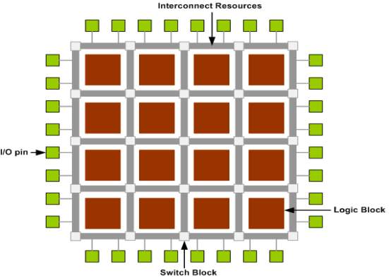
Figure 5.3 Internal structure of FPGA
Custom ICs are costly and sets aside long opportunity to plan so they are helpful when delivered in mass sums. Be that as it may, FPGAs are anything but difficult to execute inside a brief timeframe with the assistance of Computer Aided Designing (CAD) apparatuses (in light of the fact that there is no physical format prepare, no veil making, and no IC fabricating).
A few impediments of FPGAs are, they are ease back contrasted with custom ICs as they can’t handle fluctuate complex outlines and furthermore they draw more power. Xilinx rationale obstruct of one Look Table (LUT) and one Flip Flop.
A LUT is utilized to actualize number of various usefulness. The info lines to the rationale square go into the LUT and empower it. The yield of the LUT gives the consequence of the rationale work that it actualizes and the yield of rationale piece is enlisted or unregistered yield from the LUT.SRAM is utilized to execute a LUT.A k-input rationale capacity is executed utilizing 2^k * 1 measure SRAM. Number of various conceivable capacities for k input LUT is 2^2^k.
Preferred standpoint of such design is that it underpins execution of such a large number of rationale capacities, however the detriment is uncommonly vast number of memory cells required to actualize such a rationale obstruct on the off chance that number of data sources is substantial.
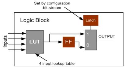
Figure 5.4 4-input LUT based usage of rationale square
In innovation mapping, the change of upgraded Boolean expression to FPGA rationale obstructs, that is said to be as Slices. Here territory and postpone improvement will be occurred. Amid situation the calculations are utilized to put each piece in FPGA cluster. Doling out the FPGA wire portions, which are programmable, to set up associations among FPGA obstructs through steering.
The arrangement of conclusive chip is made in programming unit LUT based outline accommodates better rationale piece use. A k-input LUT based rationale piece can be actualized in number of various courses with tradeoff amongst execution and rationale thickness. A n-LUT can be appeared as an immediate execution of a capacity truth-table. Each of the hooks holds the estimation of the capacity comparing to one information mix.
For Example: 2-LUT can be utilized to actualize 16 sorts of capacities like AND , OR, A +not B …. And so forth.
A B AND OR ….. …… ……
0 0 0 0
0 1 0 1
1 0 0 1
1 1 1 1
5.8 Interconnects
A wire portion can be portrayed as two end purposes of an interconnect with no programmable switch between them. A succession of at least one wire fragments in a FPGA can be named as a track.
Regularly a FPGA has rationale pieces, interconnects and switch squares (Input/yield pieces). Switch pieces lie in the outskirts of rationale squares and interconnect. Wire fragments are associated with rationale obstructs through switch squares. Contingent upon the required plan, one rationale square is associated with another et cetera.
5.9 FPGA DESIGN FLOW
In this piece of instructional exercise we will have a short introduction on FPGA configuration stream. A streamlined adaptation of configuration stream is given in the streaming outline.
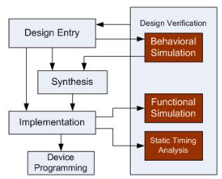
Figure 5.5 FPGA Design Flow
5.10 Outline Entry
There are diverse systems for outline passage. Schematic based, Hardware Description Language and blend of both and so on. Determination of a technique relies on upon the plan and planner. On the off chance that the fashioner needs to arrangement more with Hardware, then Schematic passage is the better decision. At the point when the outline is mind boggling or the originator thinks the plan in an algorithmic way then HDL is the better decision. Dialect based section is quicker yet slack in execution and thickness.
HDLs speak to a level of reflection that can detach the fashioners from the subtle elements of the equipment execution. Schematic based passage gives fashioners significantly more perceivability into the equipment. It is the better decision for the individuals who are equipment situated. Another strategy yet once in a while utilized is state-machines.
It is the better decision for the planners who think the outline as a progression of states. In any case, the devices for state machine section are constrained. In this documentation we will manage the HDL based outline section.
5.11 Synthesis
The procedure which deciphers VHDL or Verilog code into a gadget net list organize. i.e. a total circuit with intelligent components( entryways, flip lemon, etc) for the outline. On the off chance that the outline contains more than one sub plans, ex. to actualize a processor, we require a CPU as one plan component and RAM as another et cetera, then the union procedure creates netlist for each outline component Synthesis process will check code grammar and break down the progressive system of the outline which guarantees that the outline is upgraded for the outline engineering, the fashioner has chosen. The subsequent net list(s) is spared to a NGC( Native Generic Circuit) record (for Xilinxâ® Synthesis Technology (XST)).

Figure 5.6 FPGA Synthesis
5.12 Implementation
Usage:
In this work, outline of a DWT and IDWT is made utilizing Verilog HDL and is integrated on FPGA group of Spartan 3E through XILINX ISE Tool. This procedure incorporates taking after:
Decipher
Outline
Place and Route
5.12.1 Translate
Handle joins all the information net lists and limitations to a rationale configuration record. This data is spared as a NGD (Native Generic Database) document. This should be possible utilizing NGD Build program. Here, characterizing limitations is only, allotting the ports in the outline to the physical components (ex. pins, switches, catches and so forth) of the focused on gadget and determining time prerequisites of the plan. This data is put away in a record named UCF (User Constraints File). Devices used to make or adjust the UCF are PACE, Constraint Editor and so forth.
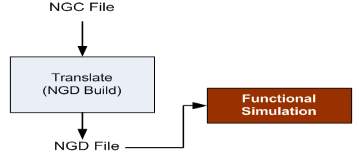
Figure 5.7FPGA Translate
5.12.2 Outline
Handle partitions the entire circuit with coherent components into sub squares to such an extent that they can be fit into the FPGA rationale pieces. That implies delineate fits the rationale characterized by the NGD record into the focused on FPGA components (Combinational Logic Blocks (CLB), Input Output Blocks (IOB)) and produces a NCD (Native Circuit Description) document which physically speaks to the plan mapped to the parts of FPGA.
Outline is utilized for this reason

Figure 5.8 PGA map
5.12.3 Place and Route
Standard program is utilized for this procedure. The place and course handle puts the sub obstructs from the guide procedure into rationale hinders as per the limitations and interfaces the rationale pieces. Ex. in the event that a sub piece is put in a rationale square which is extremely close to IO stick, then it might spare the time however it might influence some other limitation.
So tradeoff between every one of the limitations is considered by the place and course handle
The PAR device takes the mapped NCD document as info and produces a totally directed NCD record as yield. Yield NCD record comprises the directing data.
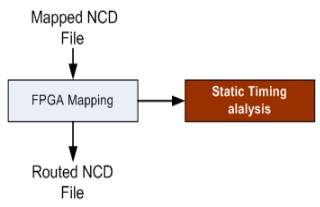
Figure 5.9 FPGA Place and route
5.13 Device Programming
Now the design must be loaded on the FPGA. But the design must be converted to a format so that the FPGA can accept it. BITGEN program deals with the conversion. The routed NCD file is then given to the BITGEN program to generate a bit stream (a .BIT file) which can be used to configure the target FPGA device. This can be done using a cable. Selection of cable depends on the design.
5.13.1 Design Verification
Verification can be done at different stages of the process steps.
5.13.2 Behavioral Simulation (RTL Simulation)
This is first of all simulation steps; those are encountered throughout the hierarchy of the design flow. This simulation is performed before synthesis process to verify RTL (behavioral) code and to confirm that the design is functioning as intended.
Behavioral simulation can be performed on either VHDL or Verilog designs. In this process, signals and variables are observed, procedures and functions are traced and breakpoints are set.
This is a very fast simulation and so allows the designer to change the HDL code if the required functionality is not met with in a short time period. Since the design is not yet synthesized to gate level, timing and resource usage properties are still unknown.
5.13.3 Functional simulation (Post Translate Simulation)
Functional simulation gives information about the logic operation of the circuit. Designer can verify the functionality of the design using this process after the Translate process. If the functionality is not as expected, then the designer has to made changes in the code and again follow the design flow steps.
Static Timing Analysis:
This can be done after MAP or PAR processes Post MAP timing report lists signal path delays of the design derived from the design logic. Post Place and Route timing report incorporates timing delay information to provide a comprehensive timing summary of the design.
CHAPTER 6: RESULTS
6.1 SIMULATION RESULT
Simulation Results of CRC remover
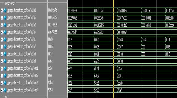
Simulation results of top module
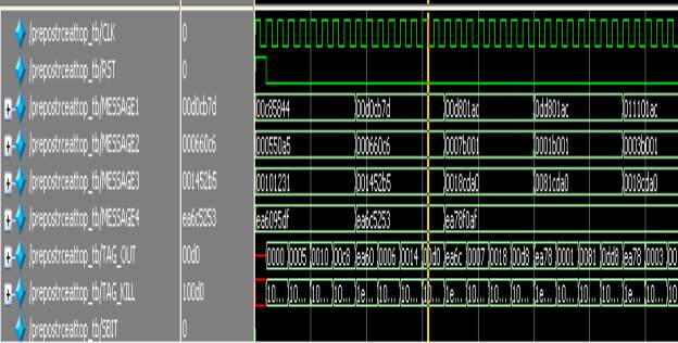
6.2 SYNTHESIS RESULTS
The developed project is reproduced and checked their usefulness. Once the practical confirmation is done, the RTL model is taken to the union procedure utilizing the Xilinx ISE instrument. In blend handle, the RTL model will be changed over to the entryway level net list mapped to a particular innovation library. Here in this Spartan 3E family, a wide range of gadgets were accessible in the Xilinx ISE instrument. To amalgamation this plan the gadget named as “XC3S500E†has been picked and the bundle as “FG320 with the gadget speed, for example, “-4”.
This plan is synthesized and its results were analyzed as follows
RTL SCHEMATIC:
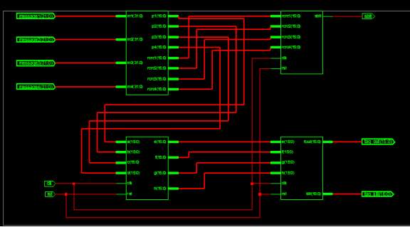
DESIGN SUMMARY:
Device summary
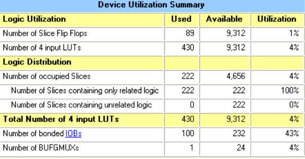
CHAPTER 7: CONCLUSION
A novel trusted key distribution server based high security scheme for RFID based system has been proposed and implemented in this work. Where communication system is abruptly disturbed/ unavailable, this security scheme provides ultimate security of information and person. Application of RFID is now in advance stage in defense and military and other high ends, this scheme are useful to protect data and access data securely. FPGA implementation of this scheme provides a single chip solution with minimum hardware, high speed operation with negligible power consumption.
REFERENCES
[1] http://www.rfidjournal.com, RFID Journal FAQs,
[2] http://www.aimglobal.org, The history of RFID, Association for Automatic Identification and Mobility, October 2001.
[3] http://www.eetimes.com. E E Times, 19 December 2001, Euro bank notes to embed RFID chips by 2005,
[4] http://www.afcea.org. Radio frequency identification ready to deliver, Signal Magazine, January 2005, Armed Forces Communications and Electronics Association (AFCEA),
[5] http://www.rsasecurity.com. RSA Laboratories, Technical characteristics of RFID,
[6] Joyashree Bag and Subir Kumar Sarkar “Design and VLSI Implementation of a Data Security scheme for RFID system using Programmable Cellular Automata” Published in the Int. Journal of RFID technology and Applications, Inderscience, IJRFITA].Pages:197-211, 2013.
[7] Joyashree Bag, Subhashis Roy and Subir Kumar Sarkar, “Advanced Multi-step Security Scheme(AMSS) using PCA for RFID system and its FPGA Implementation” [accepted, Int. Journal of RFID technology and Applications, Inderscience, IJRFITA, 2014]
[8] T. K. York, Ph. Tsalides, B. Srisuchinwong, P. J. Hicks, and A.Thanailakis, “Design and VLSI implementation of a mod- 127 multiplier using cellular automaton-based data compression techniques,” in IEEE Proc. E. Comput. Digit. Tech., vol. 138, no. 5, pp. 351-356. 1991
[9] P. D. Hortensius, R. D. Mcleod, W. Pries, D. M. Miller, and H. C.Card, “Cellular automata based pseudorandom number generators for built-in self-test,” IEEE Trans. Cornput.-Aided Design, vol. 8, no 8, pp.842-59, Aug. 1989.
[10] P. Tzionas, Ph. Tsalides, and A. Thanailakis, “Design and VLSI implementation of a pattern classifier using pseudo @D cellular automata,” IEE Proc. G, vol. 139, no. 6, pp. 661-668, Dec. 1992.
[11] D. Roy Chawdhury, I. Sengupta, S. Basu, and P. Pal Chaudhuri, “Cellular automata based error correcting codes (CAECC),” IEEE Trans.Comput., vol. 43, no. 6, pp. 759-764, June 1994
[12] P. Dasgupta, S. Chottopadhyay and I. Sengupta, “An Asic for cellular automata based message authentication”. Conference proceedings of thirteenth IEEE International Conference on VLSI Design,. pp. 538 –541;2000
Cite This Work
To export a reference to this article please select a referencing stye below:
Related Services
View allRelated Content
All TagsContent relating to: "Cyber Security"
Cyber security refers to technologies and practices undertaken to protect electronics systems and devices including computers, networks, smartphones, and the data they hold, from malicious damage, theft or exploitation.
Related Articles
DMCA / Removal Request
If you are the original writer of this dissertation and no longer wish to have your work published on the UKDiss.com website then please:


