Wireless Black Box with Mems Accelerometer
Info: 25155 words (101 pages) Dissertation
Published: 16th Dec 2019
Tagged: Engineering
CHAPTER 1
1.1 INTRODUCTION TO EMBEDDED SYSTEMS
An Embedded System is a combination of computer hardware and software, and perhaps additional mechanical or other parts, designed to perform a specific function. An embedded system is a microcontroller-based, software driven, reliable, real-time control system, autonomous, or human or network interactive, operating on diverse physical variables and in diverse environments and sold into a competitive and cost conscious market.
An embedded system is not a computer system that is used primarily for processing, not a software system on PC or UNIX, not a traditional business or scientific application. High-end embedded & lower end embedded systems. High-end embedded system - Generally 32, 64 Bit Controllers used with OS. Examples Personal Digital Assistant and Mobile phones etc. Lower end embedded systems - Generally 8,16 Bit Controllers used with an minimal operating systems and hardware layout designed for the specific purpose. Examples Small controllers and devices in our everyday life like Washing Machine, Microwave Ovens, where they are embedded in.
1.2 SYSTEM DESIGN CALLS:
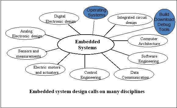 Figure 1(a): design cycles of embedded systems
EMBEDDED SYSTEM DESIGN CYCLE
Figure 1(a): design cycles of embedded systems
EMBEDDED SYSTEM DESIGN CYCLE
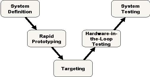 Figure.1(b):“V Diagram” of embedded systems
1.3 Characteristics of Embedded System
An embedded system is any computer system hidden inside a product other than a computer.
They will encounter a number of difficulties when writing embedded system software in addition to those we encounter when we write applications.Throughput – Our system may need to handle a lot of data in a short period of time.Response–Our system may need to react to events quickly.Testability–Setting up equipment to test embedded software can be difficult.
Debugability–Without a screen or a keyboard, finding out what the software is doing wrong (other than not working) is a troublesome problem.
Reliability – embedded systems must be able to handle any situation without human intervention
Memory space – Memory is limited on embedded systems, and you must make the software and the data fit into whatever memory exists
Program installation – you will need special tools to get your software into embedded systems
Power consumption – Portable systems must run on battery power, and the software in these systems must conserve power
Processor hogs – computing that requires large amounts of CPU time can complicate the response problem
Cost – Reducing the cost of the hardware is a concern in many embedded system projects; software often operates on hardware that is barely adequate for the job.
Embedded systems have a microprocessor/ microcontroller and a memory. Some have a serial port or a network connection. They usually do not have keyboards, screens or disk drives.
1.4 APPLICATIONS
Figure.1(b):“V Diagram” of embedded systems
1.3 Characteristics of Embedded System
An embedded system is any computer system hidden inside a product other than a computer.
They will encounter a number of difficulties when writing embedded system software in addition to those we encounter when we write applications.Throughput – Our system may need to handle a lot of data in a short period of time.Response–Our system may need to react to events quickly.Testability–Setting up equipment to test embedded software can be difficult.
Debugability–Without a screen or a keyboard, finding out what the software is doing wrong (other than not working) is a troublesome problem.
Reliability – embedded systems must be able to handle any situation without human intervention
Memory space – Memory is limited on embedded systems, and you must make the software and the data fit into whatever memory exists
Program installation – you will need special tools to get your software into embedded systems
Power consumption – Portable systems must run on battery power, and the software in these systems must conserve power
Processor hogs – computing that requires large amounts of CPU time can complicate the response problem
Cost – Reducing the cost of the hardware is a concern in many embedded system projects; software often operates on hardware that is barely adequate for the job.
Embedded systems have a microprocessor/ microcontroller and a memory. Some have a serial port or a network connection. They usually do not have keyboards, screens or disk drives.
1.4 APPLICATIONS
 CHAPTER 2
BLOCK DIAGRAM OF WIRELESS BLACKBOX
Figure.2(a):block diagram of wireless blackbox
2.1 INTRODUCTION TO WIRELESS BLACK BOX
Now a day’s accidents have become a major public problem in many countries and in metropolitan cities. This problem is due to rider's poor behaviors such as speed driving, drunk driving, riding with no helmet protection, riding without sufficient sleep, etc. Many campaigns have been conducted by the people for the awareness but the numbers of death and disability are very high because of late assistance to people those who got through the accident. Therefore, several research groups and major motorcycle manufacturers including Honda have developed safety devices to protect riders from accidental injuries.Thus, fall detection and accident alarm system for two wheelers has recently gained attention because these systems are expected to save peoples life by helping riders to get medical treatment on time. In this case, wireless black box using MEMS accelerometer and GPS tracking system is developed for accidental monitoring. If any accident occurs, this wireless device will send a message from mobile phone and indicating the position of vehicle by tracking the location through GPS system to family member, emergency medical service and nearest hospital so that they can provide ambulance and prepare treatment for the patients.
This project is to develop a wireless black box using MEMS accelerometer and GPS tracking system for accidental monitoring. MEMS is a Micro electro mechanical sensor which is a high sensitive sensor and capable of detecting the tilt. This device can perform all the tilt functions like forward, reverse, left and right directions. The system consists of cooperative components of an accelerometer, microcontroller unit, GPS device and GSM module. If any accident occurs, this wireless device will send mobile phone a short massage indicating the position of vehicle by tracing the location of the vehicle through GPS system to family member, emergency medical service (EMS) and nearest hospital. . The threshold algorithm and speed of motorcycle are used to determine fall or accident in real-time. And also at the time of occurring of accident the voices of the victims are recorded using a playback recorder so that we can use it in future to know the exact cause for the occurrence of the accident so that it would be easy for the government to find evidences.
The system consists of cooperative components of an accelerometer, microcontroller unit, GPS device, Global positioning system for Mobile module, sensors for sending a short massage. An accelerometer is applied for awareness and fall detection indicating an accident. If any accident is occurred then the location of the vehicle is traced by the longitude and latitude values of GPS and sends a SMS to the nearest hospitals and family members so that they can be ready for the treatment.
2.2 Existing system
In existing system most of the people associate black boxes with airplanes but they are no longer just the key tool in investigation of airplane accidents. Presently tracking system is introduced in vehicles to avoid the accidents and save peoples life. But these systems are still installed in some of the high-end motorcycles only because these systems are too expensive for most of the motorcycle riders. In our project we are introducing fall detection and alarm system which is expected to save peoples life by detecting the accidents occurred and provides help by tracing the location of the motorcycle riders with the help of GPS technology. This provides the information of the motorcycle rider if any accident is occurred to the family members and at the same time it sends a message to the nearest hospital for the help.
2.3 Design of proposed hardware system
The process of working of this project is explained as follows. The total equipment of this project is placed inside a vehicle is not visible to others. Here we have MEMS accelerometer which will sense the movements of the vehicle continuously. When an accident occurs to the vehicle the movement of the vehicle while the incident is occurring will be detected by the MEMS and this information is given to microcontroller. Here we use GPS module to track the location of the vehicle where the accident has occurred. GPS can get the graphical location of the vehicle and these location values are displayed on the LCD (Liquid Crystal Display). Figure.2. Block diagram of hardware system The location values are given to microcontroller. Controller gives this information to GSM module. By using GSM we can send the message to family members, emergency medical service and nearest hospital.
CHAPTER 3
HARDWARE REQUIREMENTS
HARDWARE COMPONENTS FOR WIRELESS BACKBOX:
CHAPTER 2
BLOCK DIAGRAM OF WIRELESS BLACKBOX
Figure.2(a):block diagram of wireless blackbox
2.1 INTRODUCTION TO WIRELESS BLACK BOX
Now a day’s accidents have become a major public problem in many countries and in metropolitan cities. This problem is due to rider's poor behaviors such as speed driving, drunk driving, riding with no helmet protection, riding without sufficient sleep, etc. Many campaigns have been conducted by the people for the awareness but the numbers of death and disability are very high because of late assistance to people those who got through the accident. Therefore, several research groups and major motorcycle manufacturers including Honda have developed safety devices to protect riders from accidental injuries.Thus, fall detection and accident alarm system for two wheelers has recently gained attention because these systems are expected to save peoples life by helping riders to get medical treatment on time. In this case, wireless black box using MEMS accelerometer and GPS tracking system is developed for accidental monitoring. If any accident occurs, this wireless device will send a message from mobile phone and indicating the position of vehicle by tracking the location through GPS system to family member, emergency medical service and nearest hospital so that they can provide ambulance and prepare treatment for the patients.
This project is to develop a wireless black box using MEMS accelerometer and GPS tracking system for accidental monitoring. MEMS is a Micro electro mechanical sensor which is a high sensitive sensor and capable of detecting the tilt. This device can perform all the tilt functions like forward, reverse, left and right directions. The system consists of cooperative components of an accelerometer, microcontroller unit, GPS device and GSM module. If any accident occurs, this wireless device will send mobile phone a short massage indicating the position of vehicle by tracing the location of the vehicle through GPS system to family member, emergency medical service (EMS) and nearest hospital. . The threshold algorithm and speed of motorcycle are used to determine fall or accident in real-time. And also at the time of occurring of accident the voices of the victims are recorded using a playback recorder so that we can use it in future to know the exact cause for the occurrence of the accident so that it would be easy for the government to find evidences.
The system consists of cooperative components of an accelerometer, microcontroller unit, GPS device, Global positioning system for Mobile module, sensors for sending a short massage. An accelerometer is applied for awareness and fall detection indicating an accident. If any accident is occurred then the location of the vehicle is traced by the longitude and latitude values of GPS and sends a SMS to the nearest hospitals and family members so that they can be ready for the treatment.
2.2 Existing system
In existing system most of the people associate black boxes with airplanes but they are no longer just the key tool in investigation of airplane accidents. Presently tracking system is introduced in vehicles to avoid the accidents and save peoples life. But these systems are still installed in some of the high-end motorcycles only because these systems are too expensive for most of the motorcycle riders. In our project we are introducing fall detection and alarm system which is expected to save peoples life by detecting the accidents occurred and provides help by tracing the location of the motorcycle riders with the help of GPS technology. This provides the information of the motorcycle rider if any accident is occurred to the family members and at the same time it sends a message to the nearest hospital for the help.
2.3 Design of proposed hardware system
The process of working of this project is explained as follows. The total equipment of this project is placed inside a vehicle is not visible to others. Here we have MEMS accelerometer which will sense the movements of the vehicle continuously. When an accident occurs to the vehicle the movement of the vehicle while the incident is occurring will be detected by the MEMS and this information is given to microcontroller. Here we use GPS module to track the location of the vehicle where the accident has occurred. GPS can get the graphical location of the vehicle and these location values are displayed on the LCD (Liquid Crystal Display). Figure.2. Block diagram of hardware system The location values are given to microcontroller. Controller gives this information to GSM module. By using GSM we can send the message to family members, emergency medical service and nearest hospital.
CHAPTER 3
HARDWARE REQUIREMENTS
HARDWARE COMPONENTS FOR WIRELESS BACKBOX:
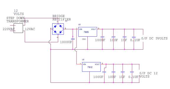 Figure.3(a):Power supply circuit for wireless blackbox
3.2 TRANSFORMER:
A transformer is a device that transfers electrical energy from one circuit to another through inductively coupled electrical conductors. A changing current in the first circuit (the primary) creates a changing magnetic field; in turn, this magnetic field induces a changing voltage in the second circuit (the secondary). By adding a load to the secondary circuit, one can make current flow in the transformer, thus transferring energy from one circuit to the other.
The secondary induced voltage VS, of an ideal transformer, is scaled from the primary VP by a factor equal to the ratio of the number of turns of wire in their respective windings:
Figure.3(a):Power supply circuit for wireless blackbox
3.2 TRANSFORMER:
A transformer is a device that transfers electrical energy from one circuit to another through inductively coupled electrical conductors. A changing current in the first circuit (the primary) creates a changing magnetic field; in turn, this magnetic field induces a changing voltage in the second circuit (the secondary). By adding a load to the secondary circuit, one can make current flow in the transformer, thus transferring energy from one circuit to the other.
The secondary induced voltage VS, of an ideal transformer, is scaled from the primary VP by a factor equal to the ratio of the number of turns of wire in their respective windings:
 The transformer is based on two principles: firstly, that an electric current can produce a magnetic field (electromagnetism) and secondly that a changing magnetic field within a coil of wire induces a voltage across the ends of the coil (electromagnetic induction). By changing the current in the primary coil, it changes the strength of its magnetic field; since the changing magnetic field extends into the secondary coil, a voltage is induced across the secondary.
A simplified transformer design is shown below. A current passing through the primary coil creates a magnetic field. The primary and secondary coils are wrapped around a core of very high magnetic permeability, such as iron; this ensures that most of the magnetic field lines produced by the primary current are within the iron and pass through the secondary coil as well as the primary coil.
The transformer is based on two principles: firstly, that an electric current can produce a magnetic field (electromagnetism) and secondly that a changing magnetic field within a coil of wire induces a voltage across the ends of the coil (electromagnetic induction). By changing the current in the primary coil, it changes the strength of its magnetic field; since the changing magnetic field extends into the secondary coil, a voltage is induced across the secondary.
A simplified transformer design is shown below. A current passing through the primary coil creates a magnetic field. The primary and secondary coils are wrapped around a core of very high magnetic permeability, such as iron; this ensures that most of the magnetic field lines produced by the primary current are within the iron and pass through the secondary coil as well as the primary coil.
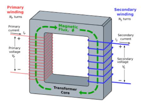 Fig.3(b):An ideal step-down transformer showing magnetic flux in the core
Induction law:The voltage induced across the secondary coil may be calculated from Faraday's law of induction, which states that:
Fig.3(b):An ideal step-down transformer showing magnetic flux in the core
Induction law:The voltage induced across the secondary coil may be calculated from Faraday's law of induction, which states that:
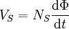 Where VS is the instantaneous voltage, NS is the number of turns in the secondary coil and Φ equals the magnetic flux through one turn of the coil. If the turns of the coil are oriented perpendicular to the magnetic field lines, the flux is the product of the magnetic field strength B and the area A through which it cuts. The area is constant, being equal to the cross-sectional area of the transformer core, whereas the magnetic field varies with time according to the excitation of the primary. Since the same magnetic flux passes through both the primary and secondary coils in an ideal transformer, the instantaneous voltage across the primary winding equals
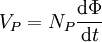 Taking the ratio of the two equations for VS and VP gives the basic equationfor stepping up or stepping down the voltage
 If the secondary coil is attached to a load that allows current to flow, electrical power is transmitted from the primary circuit to the secondary circuit. Ideally, the transformer is perfectly efficient; all the incoming energy is transformed from the primary circuit to the magnetic field and into the secondary circuit. If this condition is met, the incoming electric power must equal the outgoing power.
Pincoming = IPVP = Poutgoing = ISgiving the ideal transformer equation
If the secondary coil is attached to a load that allows current to flow, electrical power is transmitted from the primary circuit to the secondary circuit. Ideally, the transformer is perfectly efficient; all the incoming energy is transformed from the primary circuit to the magnetic field and into the secondary circuit. If this condition is met, the incoming electric power must equal the outgoing power.
Pincoming = IPVP = Poutgoing = ISgiving the ideal transformer equation
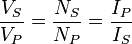
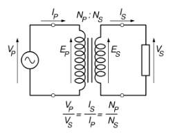 Fig.3(c):Transformer Circuit
Pin-coming = IPVP = Pout-going = ISVS
giving the ideal transformer equation
If the voltage is increased (stepped up) (VS>VP), then the current is decreased (stepped down) (IS<IP) by the same factor. Transformers are efficient so this formula is a reasonable approximation.
If the voltage is increased (stepped up) (VS>VP), then the current is decreased (stepped down) (IS<IP) by the same factor. Transformers are efficient so this formula is a reasonable approximation.
The impedance in one circuit is transformed by the square of the turns ratio. For example, if an impedance ZS is attached across the terminals of the secondary coil, it appears to the primary circuit to have an impedance of
Fig.3(c):Transformer Circuit
Pin-coming = IPVP = Pout-going = ISVS
giving the ideal transformer equation
If the voltage is increased (stepped up) (VS>VP), then the current is decreased (stepped down) (IS<IP) by the same factor. Transformers are efficient so this formula is a reasonable approximation.
If the voltage is increased (stepped up) (VS>VP), then the current is decreased (stepped down) (IS<IP) by the same factor. Transformers are efficient so this formula is a reasonable approximation.
The impedance in one circuit is transformed by the square of the turns ratio. For example, if an impedance ZS is attached across the terminals of the secondary coil, it appears to the primary circuit to have an impedance of
 This relationship is reciprocal, so that the impedance ZP of the primary circuit appears to the secondary to be
 Detailed operation:
The simplified description above neglects several practical factors, in particular the primary current required to establish a magnetic field in the core, and the contribution to the field due to current in the secondary circuit.
Models of an ideal transformer typically assume a core of negligible reluctance with two windings of zero resistance. When a voltage is applied to the primary winding, a small current flows, driving flux around the magnetic circuit of the core. The current required to create the flux is termed the magnetizing current; since the ideal core has been assumed to have near-zero reluctance, the magnetizing current is negligible, although still required to create the magnetic field.
The changing magnetic field induces an electromotive force (EMF) across each winding. Since the ideal windings have no impedance, they have no associated voltage drop, and so the voltages VP and VS measured at the terminals of the transformer, are equal to the corresponding EMFs. The primary EMF, acting as it does in opposition to the primary voltage, is sometimes termed the "back EMF". This is due to Lenz's law which states that the induction of EMF would always be such that it will oppose development of any such change in magnetic field
3.3 BRIDGE RECTIFIER
A diode bridge or bridge rectifier is an arrangement of four diodes in a bridge configuration that provides the same polarity of output voltage for any polarity of input voltage. When used in its most common application, for conversion of alternating current (AC) input into direct current (DC) output, it is known as a bridge rectifier. A bridge rectifier provides full-wave rectification from a two-wire AC input, resulting in lower cost and weight as compared to a center-tapped transformer design, but has two diode drops rather than one, thus exhibiting reduced efficiency over a center-tapped design for the same output voltage.
Basic Operation:
When the input connected at the left corner of the diamond is positive with respect to the one connected at the right hand corner, current flows to the right along the upper colored path to the output, and returns to the input supply via the lower one.
Detailed operation:
The simplified description above neglects several practical factors, in particular the primary current required to establish a magnetic field in the core, and the contribution to the field due to current in the secondary circuit.
Models of an ideal transformer typically assume a core of negligible reluctance with two windings of zero resistance. When a voltage is applied to the primary winding, a small current flows, driving flux around the magnetic circuit of the core. The current required to create the flux is termed the magnetizing current; since the ideal core has been assumed to have near-zero reluctance, the magnetizing current is negligible, although still required to create the magnetic field.
The changing magnetic field induces an electromotive force (EMF) across each winding. Since the ideal windings have no impedance, they have no associated voltage drop, and so the voltages VP and VS measured at the terminals of the transformer, are equal to the corresponding EMFs. The primary EMF, acting as it does in opposition to the primary voltage, is sometimes termed the "back EMF". This is due to Lenz's law which states that the induction of EMF would always be such that it will oppose development of any such change in magnetic field
3.3 BRIDGE RECTIFIER
A diode bridge or bridge rectifier is an arrangement of four diodes in a bridge configuration that provides the same polarity of output voltage for any polarity of input voltage. When used in its most common application, for conversion of alternating current (AC) input into direct current (DC) output, it is known as a bridge rectifier. A bridge rectifier provides full-wave rectification from a two-wire AC input, resulting in lower cost and weight as compared to a center-tapped transformer design, but has two diode drops rather than one, thus exhibiting reduced efficiency over a center-tapped design for the same output voltage.
Basic Operation:
When the input connected at the left corner of the diamond is positive with respect to the one connected at the right hand corner, current flows to the right along the upper colored path to the output, and returns to the input supply via the lower one.
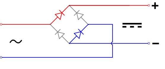 Fig.3(d):Bridge Rectifier Circuit
When the right hand corner is positive relative to the left hand corner, current flows along the upper colored path and returns to the supply via the lower colored path.
Fig.3(d):Bridge Rectifier Circuit
When the right hand corner is positive relative to the left hand corner, current flows along the upper colored path and returns to the supply via the lower colored path.
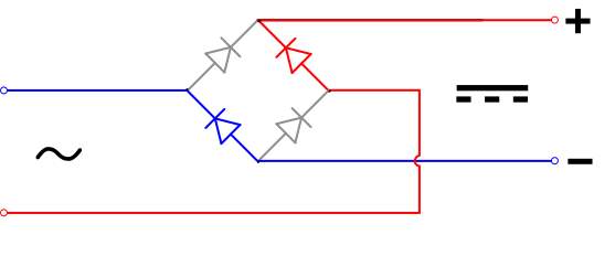 Fig.3(e):Bridge Rectifier Circuit(Right Terminal Positive)
In each case, the upper right output remains positive with respect to the lower right one. Since this is true whether the input is AC or DC, this circuit not only produces DC power when supplied with AC power: it also can provide what is sometimes called "reverse polarity protection". That is, it permits normal functioning when batteries are installed backwards or DC input-power supply wiring "has its wires crossed" (and protects the circuitry it powers against damage that might occur without this circuit in place).
Prior to availability of integrated electronics, such a bridge rectifier was always constructed from discrete components. Since about 1950, a single four-terminal component containing the four diodes connected in the bridge configuration became a standard commercial component and is now available with various voltage and current ratings.
Fig.3(e):Bridge Rectifier Circuit(Right Terminal Positive)
In each case, the upper right output remains positive with respect to the lower right one. Since this is true whether the input is AC or DC, this circuit not only produces DC power when supplied with AC power: it also can provide what is sometimes called "reverse polarity protection". That is, it permits normal functioning when batteries are installed backwards or DC input-power supply wiring "has its wires crossed" (and protects the circuitry it powers against damage that might occur without this circuit in place).
Prior to availability of integrated electronics, such a bridge rectifier was always constructed from discrete components. Since about 1950, a single four-terminal component containing the four diodes connected in the bridge configuration became a standard commercial component and is now available with various voltage and current ratings.
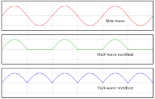 Fig.3(f):Bridge Rectifier Analysis
Output smoothing (Using Capacitor)
For many applications, especially with single phase AC where the full-wave bridge serves to convert an AC input into a DC output, the addition of a capacitor may be important because the bridge alone supplies an output voltage of fixed polarity but pulsating magnitude (see diagram above).
Fig.3(f):Bridge Rectifier Analysis
Output smoothing (Using Capacitor)
For many applications, especially with single phase AC where the full-wave bridge serves to convert an AC input into a DC output, the addition of a capacitor may be important because the bridge alone supplies an output voltage of fixed polarity but pulsating magnitude (see diagram above).
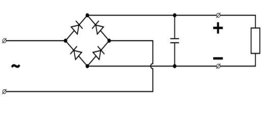 Fig.3(g):Bridge Rectifier with Output voltage
The function of this capacitor, known as a reservoir capacitor (aka smoothing capacitor) is to lessen the variation in (or 'smooth') the rectified AC output voltage waveform from the bridge. One explanation of 'smoothing' is that the capacitor provides a low impedance path to the AC component of the output, reducing the AC voltage across, and AC current through, the resistive load. In less technical terms, any drop in the output voltage and current of the bridge tends to be cancelled by loss of charge in the capacitor.
This charge flows out as additional current through the load. Thus the change of load current and voltage is reduced relative to what would occur without the capacitor. Increases of voltage correspondingly store excess charge in the capacitor, thus moderating the change in output voltage / current. Also see rectifier output smoothing.
The simplified circuit shown has a well deserved reputation for being dangerous, because, in some applications, the capacitor can retain a lethal charge after the AC power source is removed. If supplying a dangerous voltage, a practical circuit should include a reliable way to safely discharge the capacitor. If the normal load can not be guaranteed to perform this function, perhaps because it can be disconnected, the circuit should include a bleeder resistor connected as close as practical across the capacitor. This resistor should consume a current large enough to discharge the capacitor in a reasonable time, but small enough to avoid unnecessary power waste.
Because a bleeder sets a minimum current drain, the regulation of the circuit, defined as percentage voltage change from minimum to maximum load, is improved. However in many cases the improvement is of insignificant magnitude.
The capacitor and the load resistance have a typical time constant τ = RC where C and R are the capacitance and load resistance respectively. As long as the load resistor is large enough so that this time constant is much longer than the time of one ripple cycle, the above configuration will produce a smoothed DC voltage across the load.
In some designs, a series resistor at the load side of the capacitor is added. The smoothing can then be improved by adding additional stages of capacitor–resistor pairs, often done only for sub-supplies to critical high-gain circuits that tend to be sensitive to supply voltage noise.
The idealized waveforms shown above are seen for both voltage and current when the load on the bridge is resistive. When the load includes a smoothing capacitor, both the voltage and the current waveforms will be greatly changed. While the voltage is smoothed, as described above, current will flow through the bridge only during the time when the input voltage is greater than the capacitor voltage. For example, if the load draws an average current of n Amps, and the diodes conduct for 10% of the time, the average diode current during conduction must be 10n Amps. This non-sinusoidal current leads to harmonic distortion and a poor power factor in the AC supply.
In a practical circuit, when a capacitor is directly connected to the output of a bridge, the bridge diodes must be sized to withstand the current surge that occurs when the power is turned on at the peak of the AC voltage and the capacitor is fully discharged. Sometimes a small series resistor is included before the capacitor to limit this current, though in most applications the power supply transformer's resistance is already sufficient.
Output can also be smoothed using a choke and second capacitor. The choke tends to keep the current (rather than the voltage) more constant. Due to the relatively high cost of an effective choke compared to a resistor and capacitor this is not employed in modern equipment.
Some early console radios created the speaker's constant field with the current from the high voltage ("B +") power supply, which was then routed to the consuming circuits, (permanent magnets were considered too weak for good performance) to create the speaker's constant magnetic field. The speaker field coil thus performed 2 jobs in one: it acted as a choke, filtering the power supply, and it produced the magnetic field to operate the speaker.
3.4 VOLTAGE REGULATOR 7805
Features
• Output Current up to 1A.
• Output Voltages of 5, 6, 8, 9, 10, 12, 15, 18, 24V.
• Thermal Overload Protection.
• Short Circuit Protection.
• Output Transistor Safe Operating Area Protection.
Fig.3(g):Bridge Rectifier with Output voltage
The function of this capacitor, known as a reservoir capacitor (aka smoothing capacitor) is to lessen the variation in (or 'smooth') the rectified AC output voltage waveform from the bridge. One explanation of 'smoothing' is that the capacitor provides a low impedance path to the AC component of the output, reducing the AC voltage across, and AC current through, the resistive load. In less technical terms, any drop in the output voltage and current of the bridge tends to be cancelled by loss of charge in the capacitor.
This charge flows out as additional current through the load. Thus the change of load current and voltage is reduced relative to what would occur without the capacitor. Increases of voltage correspondingly store excess charge in the capacitor, thus moderating the change in output voltage / current. Also see rectifier output smoothing.
The simplified circuit shown has a well deserved reputation for being dangerous, because, in some applications, the capacitor can retain a lethal charge after the AC power source is removed. If supplying a dangerous voltage, a practical circuit should include a reliable way to safely discharge the capacitor. If the normal load can not be guaranteed to perform this function, perhaps because it can be disconnected, the circuit should include a bleeder resistor connected as close as practical across the capacitor. This resistor should consume a current large enough to discharge the capacitor in a reasonable time, but small enough to avoid unnecessary power waste.
Because a bleeder sets a minimum current drain, the regulation of the circuit, defined as percentage voltage change from minimum to maximum load, is improved. However in many cases the improvement is of insignificant magnitude.
The capacitor and the load resistance have a typical time constant τ = RC where C and R are the capacitance and load resistance respectively. As long as the load resistor is large enough so that this time constant is much longer than the time of one ripple cycle, the above configuration will produce a smoothed DC voltage across the load.
In some designs, a series resistor at the load side of the capacitor is added. The smoothing can then be improved by adding additional stages of capacitor–resistor pairs, often done only for sub-supplies to critical high-gain circuits that tend to be sensitive to supply voltage noise.
The idealized waveforms shown above are seen for both voltage and current when the load on the bridge is resistive. When the load includes a smoothing capacitor, both the voltage and the current waveforms will be greatly changed. While the voltage is smoothed, as described above, current will flow through the bridge only during the time when the input voltage is greater than the capacitor voltage. For example, if the load draws an average current of n Amps, and the diodes conduct for 10% of the time, the average diode current during conduction must be 10n Amps. This non-sinusoidal current leads to harmonic distortion and a poor power factor in the AC supply.
In a practical circuit, when a capacitor is directly connected to the output of a bridge, the bridge diodes must be sized to withstand the current surge that occurs when the power is turned on at the peak of the AC voltage and the capacitor is fully discharged. Sometimes a small series resistor is included before the capacitor to limit this current, though in most applications the power supply transformer's resistance is already sufficient.
Output can also be smoothed using a choke and second capacitor. The choke tends to keep the current (rather than the voltage) more constant. Due to the relatively high cost of an effective choke compared to a resistor and capacitor this is not employed in modern equipment.
Some early console radios created the speaker's constant field with the current from the high voltage ("B +") power supply, which was then routed to the consuming circuits, (permanent magnets were considered too weak for good performance) to create the speaker's constant magnetic field. The speaker field coil thus performed 2 jobs in one: it acted as a choke, filtering the power supply, and it produced the magnetic field to operate the speaker.
3.4 VOLTAGE REGULATOR 7805
Features
• Output Current up to 1A.
• Output Voltages of 5, 6, 8, 9, 10, 12, 15, 18, 24V.
• Thermal Overload Protection.
• Short Circuit Protection.
• Output Transistor Safe Operating Area Protection.
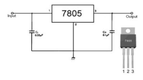 Fig.3(h):Voltage Regulator Circuit
Description
The LM78XX/LM78XXA series of three-terminal positive regulators are available in the TO-220/D-PAK package and with several fixed output voltages, making them useful in a Wide range of applications. Each type employs internal current limiting, thermal shutdown and safe operating area protection, making it essentially indestructible. If adequate heat sinking is provided, they can deliver over 1A output Current. Although designed primarily as fixed voltage regulators, these devices can be used with external components to obtain adjustable voltages and currents.
Fig.3(h):Voltage Regulator Circuit
Description
The LM78XX/LM78XXA series of three-terminal positive regulators are available in the TO-220/D-PAK package and with several fixed output voltages, making them useful in a Wide range of applications. Each type employs internal current limiting, thermal shutdown and safe operating area protection, making it essentially indestructible. If adequate heat sinking is provided, they can deliver over 1A output Current. Although designed primarily as fixed voltage regulators, these devices can be used with external components to obtain adjustable voltages and currents.
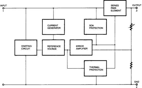 Fig.3(i):Block diagram of voltage regulator
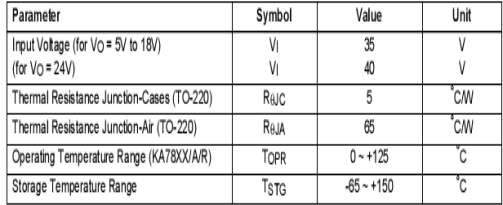
TABLE 3(a):Ratings of the voltage regulator
Fig.3(i):Block diagram of voltage regulator
TABLE 3(a):Ratings of the voltage regulator
 3.5 RECTIFIER
A rectifier is an electrical device that converts alternating current (AC), which periodically reverses direction, to direct current (DC), current that flows in only one direction, a process known as rectification. Rectifiers have many uses including as components of power supplies and as detectors of radio signals. Rectifiers may be made of solid statediodes, vacuum tube diodes, mercury arc valves, and other components. The output from the transformer is fed to the rectifier. It converts A.C. into pulsating D.C. The rectifier may be a half wave or a full wave rectifier. In this project, a bridge rectifier is used because of its merits like good stability and full wave rectification. In positive half cycleonly two diodes( 1 set of parallel diodes) will conduct, in negative half cycle remaining two diodes will conduct and they will conduct only in forward bias only.
3.5 RECTIFIER
A rectifier is an electrical device that converts alternating current (AC), which periodically reverses direction, to direct current (DC), current that flows in only one direction, a process known as rectification. Rectifiers have many uses including as components of power supplies and as detectors of radio signals. Rectifiers may be made of solid statediodes, vacuum tube diodes, mercury arc valves, and other components. The output from the transformer is fed to the rectifier. It converts A.C. into pulsating D.C. The rectifier may be a half wave or a full wave rectifier. In this project, a bridge rectifier is used because of its merits like good stability and full wave rectification. In positive half cycleonly two diodes( 1 set of parallel diodes) will conduct, in negative half cycle remaining two diodes will conduct and they will conduct only in forward bias only.
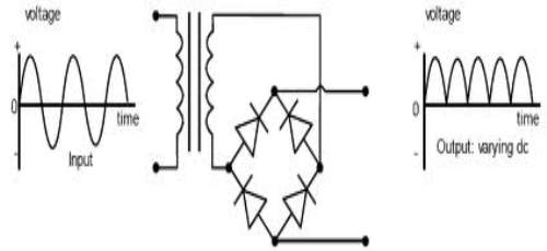 Fig.3(j):Full Wave Rectifier
3.6 FILTER
Capacitive filter is used in this project. It removes the ripples from the output of rectifier and smoothens the D.C. Output received from this filter is constant until the mains voltage and load is maintained constant. However, if either of the two is varied, D.C. voltage received at this point changes. Therefore a regulator is applied at the output stage.
The simple capacitor filter is the most basic type of power supply filter. The use of this filter is very limited. It is sometimes used on extremely high-voltage, low-current power supplies for cathode-ray and similar electron tubes that require very little load current from the supply. This filter is also used in circuits where the power-supply ripple frequency is not critical and can be relatively high. Below figure can show how the capacitor changes and discharges.
Fig.3(j):Full Wave Rectifier
3.6 FILTER
Capacitive filter is used in this project. It removes the ripples from the output of rectifier and smoothens the D.C. Output received from this filter is constant until the mains voltage and load is maintained constant. However, if either of the two is varied, D.C. voltage received at this point changes. Therefore a regulator is applied at the output stage.
The simple capacitor filter is the most basic type of power supply filter. The use of this filter is very limited. It is sometimes used on extremely high-voltage, low-current power supplies for cathode-ray and similar electron tubes that require very little load current from the supply. This filter is also used in circuits where the power-supply ripple frequency is not critical and can be relatively high. Below figure can show how the capacitor changes and discharges.
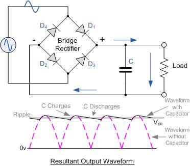 Fig.3(k):output waveform from filter
3.7 LPC 2148 ARM MICROCONTROLLER
3.7.1GENERAL DESCRIPTION OF LPC 2148:
The LPC2148 microcontrollers are based on a 16-bit/32-bit ARM7TDMI-CPU with real-time emulation and embedded trace support, that combine microcontroller with embedded high speed flash memory ranging from 32 kB to 512 kB. A 128-bit wide memory interface and unique accelerator architecture enable 32-bit code execution at the maximum clock rate. For critical code size applications, the alternative 16-bit Thumb mode reduces code by more than 30 % with minimal performance penalty. Due to their tiny size and low power consumption, LPC2148 are ideal for applications where miniaturization is a key requirement, such as access control and point-of-sale. Serial communications interfaces ranging from a USB 2.0 Full-speed device, multiple UARTs, SPI, SSP to I2C-bus and on-chip SRAM of 8 kB up to 40 kB, make these devices very well suited for communication gateways and protocol converters, soft modems, voice recognition and low end imaging, providing both large buffer size and high processing power. Various 32-bit timers, single or dual 10-bit ADC(s), 10-bit DAC, PWM channels and 45 fast GPIO lines with up to nine edge or level sensitive external interrupt pins make these microcontrollers suitable for industrial control and medical systems.
Key features:
16-bit/32-bit ARM7TDMI-S microcontroller in a tiny LQFP64 package.8 kB to 40 kB of on-chip static RAM and 32 kB to 512 kB of on-chip flash memory.128-bit wide interface/accelerator enables high-speed 60 MHz operation.In-System Programming/In-Application Programming (ISP/IAP) via on-chip boot loaderSoftware. Single flash sector or full chip erase in 400 ms and programming of256 bytes in 1 ms.Embedded ICE RT and Embedded Trace interfaces offer real-time debugging with the On-chip Real Monitor software and high-speed tracing of instruction execution.USB 2.0 Full-speed compliant device controller with 2 kB of endpoint RAM.Inaddition,the LPC2146/48 provides 8 kB of on-chip RAM accessible to USB by DMA.One or two (LPC2141/42 vs. LPC2144/46/48) 10-bit ADCs provide a total of 6/14 analog inputs, with conversion times as low as 2.44 μs per channel.Single 10-bit DAC provides variable analog output (LPC2142/44/46/48 only). Two 32-bit timers/external event counters (with four capture and four compare Vectored Interrupt Controller (VIC) with configurable priorities and vector addresses.Up to 45 of 5 V tolerant fast general purpose I/O pins in a tiny LQFP64 package. Up to 21 external interrupt pins available.60 MHz maximum CPU clock available from programmable on-chip PLL with settling Time of 100 μs.On-chip integrated oscillator operates with an external crystal from 1 MHz to 25 MHz.Power saving modes include Idle and Power-down.Individual enable/disable of peripheral functions as well as peripheral clock scaling for Additional power optimization.Processor wake-up from Power-down mode via external interrupt or BOD.
Fig.3(k):output waveform from filter
3.7 LPC 2148 ARM MICROCONTROLLER
3.7.1GENERAL DESCRIPTION OF LPC 2148:
The LPC2148 microcontrollers are based on a 16-bit/32-bit ARM7TDMI-CPU with real-time emulation and embedded trace support, that combine microcontroller with embedded high speed flash memory ranging from 32 kB to 512 kB. A 128-bit wide memory interface and unique accelerator architecture enable 32-bit code execution at the maximum clock rate. For critical code size applications, the alternative 16-bit Thumb mode reduces code by more than 30 % with minimal performance penalty. Due to their tiny size and low power consumption, LPC2148 are ideal for applications where miniaturization is a key requirement, such as access control and point-of-sale. Serial communications interfaces ranging from a USB 2.0 Full-speed device, multiple UARTs, SPI, SSP to I2C-bus and on-chip SRAM of 8 kB up to 40 kB, make these devices very well suited for communication gateways and protocol converters, soft modems, voice recognition and low end imaging, providing both large buffer size and high processing power. Various 32-bit timers, single or dual 10-bit ADC(s), 10-bit DAC, PWM channels and 45 fast GPIO lines with up to nine edge or level sensitive external interrupt pins make these microcontrollers suitable for industrial control and medical systems.
Key features:
16-bit/32-bit ARM7TDMI-S microcontroller in a tiny LQFP64 package.8 kB to 40 kB of on-chip static RAM and 32 kB to 512 kB of on-chip flash memory.128-bit wide interface/accelerator enables high-speed 60 MHz operation.In-System Programming/In-Application Programming (ISP/IAP) via on-chip boot loaderSoftware. Single flash sector or full chip erase in 400 ms and programming of256 bytes in 1 ms.Embedded ICE RT and Embedded Trace interfaces offer real-time debugging with the On-chip Real Monitor software and high-speed tracing of instruction execution.USB 2.0 Full-speed compliant device controller with 2 kB of endpoint RAM.Inaddition,the LPC2146/48 provides 8 kB of on-chip RAM accessible to USB by DMA.One or two (LPC2141/42 vs. LPC2144/46/48) 10-bit ADCs provide a total of 6/14 analog inputs, with conversion times as low as 2.44 μs per channel.Single 10-bit DAC provides variable analog output (LPC2142/44/46/48 only). Two 32-bit timers/external event counters (with four capture and four compare Vectored Interrupt Controller (VIC) with configurable priorities and vector addresses.Up to 45 of 5 V tolerant fast general purpose I/O pins in a tiny LQFP64 package. Up to 21 external interrupt pins available.60 MHz maximum CPU clock available from programmable on-chip PLL with settling Time of 100 μs.On-chip integrated oscillator operates with an external crystal from 1 MHz to 25 MHz.Power saving modes include Idle and Power-down.Individual enable/disable of peripheral functions as well as peripheral clock scaling for Additional power optimization.Processor wake-up from Power-down mode via external interrupt or BOD.
Figure 1(a): design cycles of embedded systems
EMBEDDED SYSTEM DESIGN CYCLE
Figure.1(b):“V Diagram” of embedded systems
1.3 Characteristics of Embedded System
An embedded system is any computer system hidden inside a product other than a computer.
They will encounter a number of difficulties when writing embedded system software in addition to those we encounter when we write applications.Throughput – Our system may need to handle a lot of data in a short period of time.Response–Our system may need to react to events quickly.Testability–Setting up equipment to test embedded software can be difficult.
Debugability–Without a screen or a keyboard, finding out what the software is doing wrong (other than not working) is a troublesome problem.
Reliability – embedded systems must be able to handle any situation without human intervention
Memory space – Memory is limited on embedded systems, and you must make the software and the data fit into whatever memory exists
Program installation – you will need special tools to get your software into embedded systems
Power consumption – Portable systems must run on battery power, and the software in these systems must conserve power
Processor hogs – computing that requires large amounts of CPU time can complicate the response problem
Cost – Reducing the cost of the hardware is a concern in many embedded system projects; software often operates on hardware that is barely adequate for the job.
Embedded systems have a microprocessor/ microcontroller and a memory. Some have a serial port or a network connection. They usually do not have keyboards, screens or disk drives.
1.4 APPLICATIONS
- Military and aerospace embedded software applications
- Communication Applications
- Industrial automation and process control software
- Mastering the complexity of applications.
- Reduction of product design time.
- Real time processing of ever increasing amounts of data.
- Intelligent, autonomous sensors.
CHAPTER 2
BLOCK DIAGRAM OF WIRELESS BLACKBOX
Figure.2(a):block diagram of wireless blackbox
2.1 INTRODUCTION TO WIRELESS BLACK BOX
Now a day’s accidents have become a major public problem in many countries and in metropolitan cities. This problem is due to rider's poor behaviors such as speed driving, drunk driving, riding with no helmet protection, riding without sufficient sleep, etc. Many campaigns have been conducted by the people for the awareness but the numbers of death and disability are very high because of late assistance to people those who got through the accident. Therefore, several research groups and major motorcycle manufacturers including Honda have developed safety devices to protect riders from accidental injuries.Thus, fall detection and accident alarm system for two wheelers has recently gained attention because these systems are expected to save peoples life by helping riders to get medical treatment on time. In this case, wireless black box using MEMS accelerometer and GPS tracking system is developed for accidental monitoring. If any accident occurs, this wireless device will send a message from mobile phone and indicating the position of vehicle by tracking the location through GPS system to family member, emergency medical service and nearest hospital so that they can provide ambulance and prepare treatment for the patients.
This project is to develop a wireless black box using MEMS accelerometer and GPS tracking system for accidental monitoring. MEMS is a Micro electro mechanical sensor which is a high sensitive sensor and capable of detecting the tilt. This device can perform all the tilt functions like forward, reverse, left and right directions. The system consists of cooperative components of an accelerometer, microcontroller unit, GPS device and GSM module. If any accident occurs, this wireless device will send mobile phone a short massage indicating the position of vehicle by tracing the location of the vehicle through GPS system to family member, emergency medical service (EMS) and nearest hospital. . The threshold algorithm and speed of motorcycle are used to determine fall or accident in real-time. And also at the time of occurring of accident the voices of the victims are recorded using a playback recorder so that we can use it in future to know the exact cause for the occurrence of the accident so that it would be easy for the government to find evidences.
The system consists of cooperative components of an accelerometer, microcontroller unit, GPS device, Global positioning system for Mobile module, sensors for sending a short massage. An accelerometer is applied for awareness and fall detection indicating an accident. If any accident is occurred then the location of the vehicle is traced by the longitude and latitude values of GPS and sends a SMS to the nearest hospitals and family members so that they can be ready for the treatment.
2.2 Existing system
In existing system most of the people associate black boxes with airplanes but they are no longer just the key tool in investigation of airplane accidents. Presently tracking system is introduced in vehicles to avoid the accidents and save peoples life. But these systems are still installed in some of the high-end motorcycles only because these systems are too expensive for most of the motorcycle riders. In our project we are introducing fall detection and alarm system which is expected to save peoples life by detecting the accidents occurred and provides help by tracing the location of the motorcycle riders with the help of GPS technology. This provides the information of the motorcycle rider if any accident is occurred to the family members and at the same time it sends a message to the nearest hospital for the help.
2.3 Design of proposed hardware system
The process of working of this project is explained as follows. The total equipment of this project is placed inside a vehicle is not visible to others. Here we have MEMS accelerometer which will sense the movements of the vehicle continuously. When an accident occurs to the vehicle the movement of the vehicle while the incident is occurring will be detected by the MEMS and this information is given to microcontroller. Here we use GPS module to track the location of the vehicle where the accident has occurred. GPS can get the graphical location of the vehicle and these location values are displayed on the LCD (Liquid Crystal Display). Figure.2. Block diagram of hardware system The location values are given to microcontroller. Controller gives this information to GSM module. By using GSM we can send the message to family members, emergency medical service and nearest hospital.
CHAPTER 3
HARDWARE REQUIREMENTS
HARDWARE COMPONENTS FOR WIRELESS BACKBOX:
- POWER SUPPLY
- TRANSFORMER (230 – 12 V AC)
- VOLTAGE REGULATOR (LM 7805)
- RECTIFIER
- FILTER
- LPC 2148 MICROCONTROLLER
- GSM MODULE
- GPS MODULE
- PUSH BUTTON
- 1N4007
- LED
- LCD
- RESISTOR
- CAPACITOR
- GPS
- LCD
Figure.3(a):Power supply circuit for wireless blackbox
3.2 TRANSFORMER:
A transformer is a device that transfers electrical energy from one circuit to another through inductively coupled electrical conductors. A changing current in the first circuit (the primary) creates a changing magnetic field; in turn, this magnetic field induces a changing voltage in the second circuit (the secondary). By adding a load to the secondary circuit, one can make current flow in the transformer, thus transferring energy from one circuit to the other.
The secondary induced voltage VS, of an ideal transformer, is scaled from the primary VP by a factor equal to the ratio of the number of turns of wire in their respective windings:
The transformer is based on two principles: firstly, that an electric current can produce a magnetic field (electromagnetism) and secondly that a changing magnetic field within a coil of wire induces a voltage across the ends of the coil (electromagnetic induction). By changing the current in the primary coil, it changes the strength of its magnetic field; since the changing magnetic field extends into the secondary coil, a voltage is induced across the secondary.
A simplified transformer design is shown below. A current passing through the primary coil creates a magnetic field. The primary and secondary coils are wrapped around a core of very high magnetic permeability, such as iron; this ensures that most of the magnetic field lines produced by the primary current are within the iron and pass through the secondary coil as well as the primary coil.
 Fig.3(b):An ideal step-down transformer showing magnetic flux in the core
Induction law:The voltage induced across the secondary coil may be calculated from Faraday's law of induction, which states that:
Where VS is the instantaneous voltage, NS is the number of turns in the secondary coil and Φ equals the magnetic flux through one turn of the coil. If the turns of the coil are oriented perpendicular to the magnetic field lines, the flux is the product of the magnetic field strength B and the area A through which it cuts. The area is constant, being equal to the cross-sectional area of the transformer core, whereas the magnetic field varies with time according to the excitation of the primary. Since the same magnetic flux passes through both the primary and secondary coils in an ideal transformer, the instantaneous voltage across the primary winding equals
Taking the ratio of the two equations for VS and VP gives the basic equationfor stepping up or stepping down the voltage
If the secondary coil is attached to a load that allows current to flow, electrical power is transmitted from the primary circuit to the secondary circuit. Ideally, the transformer is perfectly efficient; all the incoming energy is transformed from the primary circuit to the magnetic field and into the secondary circuit. If this condition is met, the incoming electric power must equal the outgoing power.
Pincoming = IPVP = Poutgoing = ISgiving the ideal transformer equation
Fig.3(b):An ideal step-down transformer showing magnetic flux in the core
Induction law:The voltage induced across the secondary coil may be calculated from Faraday's law of induction, which states that:
Where VS is the instantaneous voltage, NS is the number of turns in the secondary coil and Φ equals the magnetic flux through one turn of the coil. If the turns of the coil are oriented perpendicular to the magnetic field lines, the flux is the product of the magnetic field strength B and the area A through which it cuts. The area is constant, being equal to the cross-sectional area of the transformer core, whereas the magnetic field varies with time according to the excitation of the primary. Since the same magnetic flux passes through both the primary and secondary coils in an ideal transformer, the instantaneous voltage across the primary winding equals
Taking the ratio of the two equations for VS and VP gives the basic equationfor stepping up or stepping down the voltage
If the secondary coil is attached to a load that allows current to flow, electrical power is transmitted from the primary circuit to the secondary circuit. Ideally, the transformer is perfectly efficient; all the incoming energy is transformed from the primary circuit to the magnetic field and into the secondary circuit. If this condition is met, the incoming electric power must equal the outgoing power.
Pincoming = IPVP = Poutgoing = ISgiving the ideal transformer equation
 Fig.3(c):Transformer Circuit
Pin-coming = IPVP = Pout-going = ISVS
giving the ideal transformer equation
If the voltage is increased (stepped up) (VS>VP), then the current is decreased (stepped down) (IS<IP) by the same factor. Transformers are efficient so this formula is a reasonable approximation.
If the voltage is increased (stepped up) (VS>VP), then the current is decreased (stepped down) (IS<IP) by the same factor. Transformers are efficient so this formula is a reasonable approximation.
The impedance in one circuit is transformed by the square of the turns ratio. For example, if an impedance ZS is attached across the terminals of the secondary coil, it appears to the primary circuit to have an impedance of
This relationship is reciprocal, so that the impedance ZP of the primary circuit appears to the secondary to be
Detailed operation:
The simplified description above neglects several practical factors, in particular the primary current required to establish a magnetic field in the core, and the contribution to the field due to current in the secondary circuit.
Models of an ideal transformer typically assume a core of negligible reluctance with two windings of zero resistance. When a voltage is applied to the primary winding, a small current flows, driving flux around the magnetic circuit of the core. The current required to create the flux is termed the magnetizing current; since the ideal core has been assumed to have near-zero reluctance, the magnetizing current is negligible, although still required to create the magnetic field.
The changing magnetic field induces an electromotive force (EMF) across each winding. Since the ideal windings have no impedance, they have no associated voltage drop, and so the voltages VP and VS measured at the terminals of the transformer, are equal to the corresponding EMFs. The primary EMF, acting as it does in opposition to the primary voltage, is sometimes termed the "back EMF". This is due to Lenz's law which states that the induction of EMF would always be such that it will oppose development of any such change in magnetic field
3.3 BRIDGE RECTIFIER
A diode bridge or bridge rectifier is an arrangement of four diodes in a bridge configuration that provides the same polarity of output voltage for any polarity of input voltage. When used in its most common application, for conversion of alternating current (AC) input into direct current (DC) output, it is known as a bridge rectifier. A bridge rectifier provides full-wave rectification from a two-wire AC input, resulting in lower cost and weight as compared to a center-tapped transformer design, but has two diode drops rather than one, thus exhibiting reduced efficiency over a center-tapped design for the same output voltage.
Basic Operation:
When the input connected at the left corner of the diamond is positive with respect to the one connected at the right hand corner, current flows to the right along the upper colored path to the output, and returns to the input supply via the lower one.
Fig.3(c):Transformer Circuit
Pin-coming = IPVP = Pout-going = ISVS
giving the ideal transformer equation
If the voltage is increased (stepped up) (VS>VP), then the current is decreased (stepped down) (IS<IP) by the same factor. Transformers are efficient so this formula is a reasonable approximation.
If the voltage is increased (stepped up) (VS>VP), then the current is decreased (stepped down) (IS<IP) by the same factor. Transformers are efficient so this formula is a reasonable approximation.
The impedance in one circuit is transformed by the square of the turns ratio. For example, if an impedance ZS is attached across the terminals of the secondary coil, it appears to the primary circuit to have an impedance of
This relationship is reciprocal, so that the impedance ZP of the primary circuit appears to the secondary to be
Detailed operation:
The simplified description above neglects several practical factors, in particular the primary current required to establish a magnetic field in the core, and the contribution to the field due to current in the secondary circuit.
Models of an ideal transformer typically assume a core of negligible reluctance with two windings of zero resistance. When a voltage is applied to the primary winding, a small current flows, driving flux around the magnetic circuit of the core. The current required to create the flux is termed the magnetizing current; since the ideal core has been assumed to have near-zero reluctance, the magnetizing current is negligible, although still required to create the magnetic field.
The changing magnetic field induces an electromotive force (EMF) across each winding. Since the ideal windings have no impedance, they have no associated voltage drop, and so the voltages VP and VS measured at the terminals of the transformer, are equal to the corresponding EMFs. The primary EMF, acting as it does in opposition to the primary voltage, is sometimes termed the "back EMF". This is due to Lenz's law which states that the induction of EMF would always be such that it will oppose development of any such change in magnetic field
3.3 BRIDGE RECTIFIER
A diode bridge or bridge rectifier is an arrangement of four diodes in a bridge configuration that provides the same polarity of output voltage for any polarity of input voltage. When used in its most common application, for conversion of alternating current (AC) input into direct current (DC) output, it is known as a bridge rectifier. A bridge rectifier provides full-wave rectification from a two-wire AC input, resulting in lower cost and weight as compared to a center-tapped transformer design, but has two diode drops rather than one, thus exhibiting reduced efficiency over a center-tapped design for the same output voltage.
Basic Operation:
When the input connected at the left corner of the diamond is positive with respect to the one connected at the right hand corner, current flows to the right along the upper colored path to the output, and returns to the input supply via the lower one.
 Fig.3(d):Bridge Rectifier Circuit
When the right hand corner is positive relative to the left hand corner, current flows along the upper colored path and returns to the supply via the lower colored path.
Fig.3(d):Bridge Rectifier Circuit
When the right hand corner is positive relative to the left hand corner, current flows along the upper colored path and returns to the supply via the lower colored path.
 Fig.3(e):Bridge Rectifier Circuit(Right Terminal Positive)
In each case, the upper right output remains positive with respect to the lower right one. Since this is true whether the input is AC or DC, this circuit not only produces DC power when supplied with AC power: it also can provide what is sometimes called "reverse polarity protection". That is, it permits normal functioning when batteries are installed backwards or DC input-power supply wiring "has its wires crossed" (and protects the circuitry it powers against damage that might occur without this circuit in place).
Prior to availability of integrated electronics, such a bridge rectifier was always constructed from discrete components. Since about 1950, a single four-terminal component containing the four diodes connected in the bridge configuration became a standard commercial component and is now available with various voltage and current ratings.
Fig.3(e):Bridge Rectifier Circuit(Right Terminal Positive)
In each case, the upper right output remains positive with respect to the lower right one. Since this is true whether the input is AC or DC, this circuit not only produces DC power when supplied with AC power: it also can provide what is sometimes called "reverse polarity protection". That is, it permits normal functioning when batteries are installed backwards or DC input-power supply wiring "has its wires crossed" (and protects the circuitry it powers against damage that might occur without this circuit in place).
Prior to availability of integrated electronics, such a bridge rectifier was always constructed from discrete components. Since about 1950, a single four-terminal component containing the four diodes connected in the bridge configuration became a standard commercial component and is now available with various voltage and current ratings.
 Fig.3(f):Bridge Rectifier Analysis
Output smoothing (Using Capacitor)
For many applications, especially with single phase AC where the full-wave bridge serves to convert an AC input into a DC output, the addition of a capacitor may be important because the bridge alone supplies an output voltage of fixed polarity but pulsating magnitude (see diagram above).
Fig.3(f):Bridge Rectifier Analysis
Output smoothing (Using Capacitor)
For many applications, especially with single phase AC where the full-wave bridge serves to convert an AC input into a DC output, the addition of a capacitor may be important because the bridge alone supplies an output voltage of fixed polarity but pulsating magnitude (see diagram above).
 Fig.3(g):Bridge Rectifier with Output voltage
The function of this capacitor, known as a reservoir capacitor (aka smoothing capacitor) is to lessen the variation in (or 'smooth') the rectified AC output voltage waveform from the bridge. One explanation of 'smoothing' is that the capacitor provides a low impedance path to the AC component of the output, reducing the AC voltage across, and AC current through, the resistive load. In less technical terms, any drop in the output voltage and current of the bridge tends to be cancelled by loss of charge in the capacitor.
This charge flows out as additional current through the load. Thus the change of load current and voltage is reduced relative to what would occur without the capacitor. Increases of voltage correspondingly store excess charge in the capacitor, thus moderating the change in output voltage / current. Also see rectifier output smoothing.
The simplified circuit shown has a well deserved reputation for being dangerous, because, in some applications, the capacitor can retain a lethal charge after the AC power source is removed. If supplying a dangerous voltage, a practical circuit should include a reliable way to safely discharge the capacitor. If the normal load can not be guaranteed to perform this function, perhaps because it can be disconnected, the circuit should include a bleeder resistor connected as close as practical across the capacitor. This resistor should consume a current large enough to discharge the capacitor in a reasonable time, but small enough to avoid unnecessary power waste.
Because a bleeder sets a minimum current drain, the regulation of the circuit, defined as percentage voltage change from minimum to maximum load, is improved. However in many cases the improvement is of insignificant magnitude.
The capacitor and the load resistance have a typical time constant τ = RC where C and R are the capacitance and load resistance respectively. As long as the load resistor is large enough so that this time constant is much longer than the time of one ripple cycle, the above configuration will produce a smoothed DC voltage across the load.
In some designs, a series resistor at the load side of the capacitor is added. The smoothing can then be improved by adding additional stages of capacitor–resistor pairs, often done only for sub-supplies to critical high-gain circuits that tend to be sensitive to supply voltage noise.
The idealized waveforms shown above are seen for both voltage and current when the load on the bridge is resistive. When the load includes a smoothing capacitor, both the voltage and the current waveforms will be greatly changed. While the voltage is smoothed, as described above, current will flow through the bridge only during the time when the input voltage is greater than the capacitor voltage. For example, if the load draws an average current of n Amps, and the diodes conduct for 10% of the time, the average diode current during conduction must be 10n Amps. This non-sinusoidal current leads to harmonic distortion and a poor power factor in the AC supply.
In a practical circuit, when a capacitor is directly connected to the output of a bridge, the bridge diodes must be sized to withstand the current surge that occurs when the power is turned on at the peak of the AC voltage and the capacitor is fully discharged. Sometimes a small series resistor is included before the capacitor to limit this current, though in most applications the power supply transformer's resistance is already sufficient.
Output can also be smoothed using a choke and second capacitor. The choke tends to keep the current (rather than the voltage) more constant. Due to the relatively high cost of an effective choke compared to a resistor and capacitor this is not employed in modern equipment.
Some early console radios created the speaker's constant field with the current from the high voltage ("B +") power supply, which was then routed to the consuming circuits, (permanent magnets were considered too weak for good performance) to create the speaker's constant magnetic field. The speaker field coil thus performed 2 jobs in one: it acted as a choke, filtering the power supply, and it produced the magnetic field to operate the speaker.
3.4 VOLTAGE REGULATOR 7805
Features
• Output Current up to 1A.
• Output Voltages of 5, 6, 8, 9, 10, 12, 15, 18, 24V.
• Thermal Overload Protection.
• Short Circuit Protection.
• Output Transistor Safe Operating Area Protection.
Fig.3(h):Voltage Regulator Circuit
Description
The LM78XX/LM78XXA series of three-terminal positive regulators are available in the TO-220/D-PAK package and with several fixed output voltages, making them useful in a Wide range of applications. Each type employs internal current limiting, thermal shutdown and safe operating area protection, making it essentially indestructible. If adequate heat sinking is provided, they can deliver over 1A output Current. Although designed primarily as fixed voltage regulators, these devices can be used with external components to obtain adjustable voltages and currents.
Fig.3(i):Block diagram of voltage regulator
TABLE 3(a):Ratings of the voltage regulator
3.5 RECTIFIER
A rectifier is an electrical device that converts alternating current (AC), which periodically reverses direction, to direct current (DC), current that flows in only one direction, a process known as rectification. Rectifiers have many uses including as components of power supplies and as detectors of radio signals. Rectifiers may be made of solid statediodes, vacuum tube diodes, mercury arc valves, and other components. The output from the transformer is fed to the rectifier. It converts A.C. into pulsating D.C. The rectifier may be a half wave or a full wave rectifier. In this project, a bridge rectifier is used because of its merits like good stability and full wave rectification. In positive half cycleonly two diodes( 1 set of parallel diodes) will conduct, in negative half cycle remaining two diodes will conduct and they will conduct only in forward bias only.
Fig.3(j):Full Wave Rectifier
3.6 FILTER
Capacitive filter is used in this project. It removes the ripples from the output of rectifier and smoothens the D.C. Output received from this filter is constant until the mains voltage and load is maintained constant. However, if either of the two is varied, D.C. voltage received at this point changes. Therefore a regulator is applied at the output stage.
The simple capacitor filter is the most basic type of power supply filter. The use of this filter is very limited. It is sometimes used on extremely high-voltage, low-current power supplies for cathode-ray and similar electron tubes that require very little load current from the supply. This filter is also used in circuits where the power-supply ripple frequency is not critical and can be relatively high. Below figure can show how the capacitor changes and discharges.
Fig.3(k):output waveform from filter
3.7 LPC 2148 ARM MICROCONTROLLER
3.7.1GENERAL DESCRIPTION OF LPC 2148:
The LPC2148 microcontrollers are based on a 16-bit/32-bit ARM7TDMI-CPU with real-time emulation and embedded trace support, that combine microcontroller with embedded high speed flash memory ranging from 32 kB to 512 kB. A 128-bit wide memory interface and unique accelerator architecture enable 32-bit code execution at the maximum clock rate. For critical code size applications, the alternative 16-bit Thumb mode reduces code by more than 30 % with minimal performance penalty. Due to their tiny size and low power consumption, LPC2148 are ideal for applications where miniaturization is a key requirement, such as access control and point-of-sale. Serial communications interfaces ranging from a USB 2.0 Full-speed device, multiple UARTs, SPI, SSP to I2C-bus and on-chip SRAM of 8 kB up to 40 kB, make these devices very well suited for communication gateways and protocol converters, soft modems, voice recognition and low end imaging, providing both large buffer size and high processing power. Various 32-bit timers, single or dual 10-bit ADC(s), 10-bit DAC, PWM channels and 45 fast GPIO lines with up to nine edge or level sensitive external interrupt pins make these microcontrollers suitable for industrial control and medical systems.
Key features:
16-bit/32-bit ARM7TDMI-S microcontroller in a tiny LQFP64 package.8 kB to 40 kB of on-chip static RAM and 32 kB to 512 kB of on-chip flash memory.128-bit wide interface/accelerator enables high-speed 60 MHz operation.In-System Programming/In-Application Programming (ISP/IAP) via on-chip boot loaderSoftware. Single flash sector or full chip erase in 400 ms and programming of256 bytes in 1 ms.Embedded ICE RT and Embedded Trace interfaces offer real-time debugging with the On-chip Real Monitor software and high-speed tracing of instruction execution.USB 2.0 Full-speed compliant device controller with 2 kB of endpoint RAM.Inaddition,the LPC2146/48 provides 8 kB of on-chip RAM accessible to USB by DMA.One or two (LPC2141/42 vs. LPC2144/46/48) 10-bit ADCs provide a total of 6/14 analog inputs, with conversion times as low as 2.44 μs per channel.Single 10-bit DAC provides variable analog output (LPC2142/44/46/48 only). Two 32-bit timers/external event counters (with four capture and four compare Vectored Interrupt Controller (VIC) with configurable priorities and vector addresses.Up to 45 of 5 V tolerant fast general purpose I/O pins in a tiny LQFP64 package. Up to 21 external interrupt pins available.60 MHz maximum CPU clock available from programmable on-chip PLL with settling Time of 100 μs.On-chip integrated oscillator operates with an external crystal from 1 MHz to 25 MHz.Power saving modes include Idle and Power-down.Individual enable/disable of peripheral functions as well as peripheral clock scaling for Additional power optimization.Processor wake-up from Power-down mode via external interrupt or BOD.
Fig.3(g):Bridge Rectifier with Output voltage
The function of this capacitor, known as a reservoir capacitor (aka smoothing capacitor) is to lessen the variation in (or 'smooth') the rectified AC output voltage waveform from the bridge. One explanation of 'smoothing' is that the capacitor provides a low impedance path to the AC component of the output, reducing the AC voltage across, and AC current through, the resistive load. In less technical terms, any drop in the output voltage and current of the bridge tends to be cancelled by loss of charge in the capacitor.
This charge flows out as additional current through the load. Thus the change of load current and voltage is reduced relative to what would occur without the capacitor. Increases of voltage correspondingly store excess charge in the capacitor, thus moderating the change in output voltage / current. Also see rectifier output smoothing.
The simplified circuit shown has a well deserved reputation for being dangerous, because, in some applications, the capacitor can retain a lethal charge after the AC power source is removed. If supplying a dangerous voltage, a practical circuit should include a reliable way to safely discharge the capacitor. If the normal load can not be guaranteed to perform this function, perhaps because it can be disconnected, the circuit should include a bleeder resistor connected as close as practical across the capacitor. This resistor should consume a current large enough to discharge the capacitor in a reasonable time, but small enough to avoid unnecessary power waste.
Because a bleeder sets a minimum current drain, the regulation of the circuit, defined as percentage voltage change from minimum to maximum load, is improved. However in many cases the improvement is of insignificant magnitude.
The capacitor and the load resistance have a typical time constant τ = RC where C and R are the capacitance and load resistance respectively. As long as the load resistor is large enough so that this time constant is much longer than the time of one ripple cycle, the above configuration will produce a smoothed DC voltage across the load.
In some designs, a series resistor at the load side of the capacitor is added. The smoothing can then be improved by adding additional stages of capacitor–resistor pairs, often done only for sub-supplies to critical high-gain circuits that tend to be sensitive to supply voltage noise.
The idealized waveforms shown above are seen for both voltage and current when the load on the bridge is resistive. When the load includes a smoothing capacitor, both the voltage and the current waveforms will be greatly changed. While the voltage is smoothed, as described above, current will flow through the bridge only during the time when the input voltage is greater than the capacitor voltage. For example, if the load draws an average current of n Amps, and the diodes conduct for 10% of the time, the average diode current during conduction must be 10n Amps. This non-sinusoidal current leads to harmonic distortion and a poor power factor in the AC supply.
In a practical circuit, when a capacitor is directly connected to the output of a bridge, the bridge diodes must be sized to withstand the current surge that occurs when the power is turned on at the peak of the AC voltage and the capacitor is fully discharged. Sometimes a small series resistor is included before the capacitor to limit this current, though in most applications the power supply transformer's resistance is already sufficient.
Output can also be smoothed using a choke and second capacitor. The choke tends to keep the current (rather than the voltage) more constant. Due to the relatively high cost of an effective choke compared to a resistor and capacitor this is not employed in modern equipment.
Some early console radios created the speaker's constant field with the current from the high voltage ("B +") power supply, which was then routed to the consuming circuits, (permanent magnets were considered too weak for good performance) to create the speaker's constant magnetic field. The speaker field coil thus performed 2 jobs in one: it acted as a choke, filtering the power supply, and it produced the magnetic field to operate the speaker.
3.4 VOLTAGE REGULATOR 7805
Features
• Output Current up to 1A.
• Output Voltages of 5, 6, 8, 9, 10, 12, 15, 18, 24V.
• Thermal Overload Protection.
• Short Circuit Protection.
• Output Transistor Safe Operating Area Protection.
Fig.3(h):Voltage Regulator Circuit
Description
The LM78XX/LM78XXA series of three-terminal positive regulators are available in the TO-220/D-PAK package and with several fixed output voltages, making them useful in a Wide range of applications. Each type employs internal current limiting, thermal shutdown and safe operating area protection, making it essentially indestructible. If adequate heat sinking is provided, they can deliver over 1A output Current. Although designed primarily as fixed voltage regulators, these devices can be used with external components to obtain adjustable voltages and currents.
Fig.3(i):Block diagram of voltage regulator
TABLE 3(a):Ratings of the voltage regulator
3.5 RECTIFIER
A rectifier is an electrical device that converts alternating current (AC), which periodically reverses direction, to direct current (DC), current that flows in only one direction, a process known as rectification. Rectifiers have many uses including as components of power supplies and as detectors of radio signals. Rectifiers may be made of solid statediodes, vacuum tube diodes, mercury arc valves, and other components. The output from the transformer is fed to the rectifier. It converts A.C. into pulsating D.C. The rectifier may be a half wave or a full wave rectifier. In this project, a bridge rectifier is used because of its merits like good stability and full wave rectification. In positive half cycleonly two diodes( 1 set of parallel diodes) will conduct, in negative half cycle remaining two diodes will conduct and they will conduct only in forward bias only.
Fig.3(j):Full Wave Rectifier
3.6 FILTER
Capacitive filter is used in this project. It removes the ripples from the output of rectifier and smoothens the D.C. Output received from this filter is constant until the mains voltage and load is maintained constant. However, if either of the two is varied, D.C. voltage received at this point changes. Therefore a regulator is applied at the output stage.
The simple capacitor filter is the most basic type of power supply filter. The use of this filter is very limited. It is sometimes used on extremely high-voltage, low-current power supplies for cathode-ray and similar electron tubes that require very little load current from the supply. This filter is also used in circuits where the power-supply ripple frequency is not critical and can be relatively high. Below figure can show how the capacitor changes and discharges.
Fig.3(k):output waveform from filter
3.7 LPC 2148 ARM MICROCONTROLLER
3.7.1GENERAL DESCRIPTION OF LPC 2148:
The LPC2148 microcontrollers are based on a 16-bit/32-bit ARM7TDMI-CPU with real-time emulation and embedded trace support, that combine microcontroller with embedded high speed flash memory ranging from 32 kB to 512 kB. A 128-bit wide memory interface and unique accelerator architecture enable 32-bit code execution at the maximum clock rate. For critical code size applications, the alternative 16-bit Thumb mode reduces code by more than 30 % with minimal performance penalty. Due to their tiny size and low power consumption, LPC2148 are ideal for applications where miniaturization is a key requirement, such as access control and point-of-sale. Serial communications interfaces ranging from a USB 2.0 Full-speed device, multiple UARTs, SPI, SSP to I2C-bus and on-chip SRAM of 8 kB up to 40 kB, make these devices very well suited for communication gateways and protocol converters, soft modems, voice recognition and low end imaging, providing both large buffer size and high processing power. Various 32-bit timers, single or dual 10-bit ADC(s), 10-bit DAC, PWM channels and 45 fast GPIO lines with up to nine edge or level sensitive external interrupt pins make these microcontrollers suitable for industrial control and medical systems.
Key features:
16-bit/32-bit ARM7TDMI-S microcontroller in a tiny LQFP64 package.8 kB to 40 kB of on-chip static RAM and 32 kB to 512 kB of on-chip flash memory.128-bit wide interface/accelerator enables high-speed 60 MHz operation.In-System Programming/In-Application Programming (ISP/IAP) via on-chip boot loaderSoftware. Single flash sector or full chip erase in 400 ms and programming of256 bytes in 1 ms.Embedded ICE RT and Embedded Trace interfaces offer real-time debugging with the On-chip Real Monitor software and high-speed tracing of instruction execution.USB 2.0 Full-speed compliant device controller with 2 kB of endpoint RAM.Inaddition,the LPC2146/48 provides 8 kB of on-chip RAM accessible to USB by DMA.One or two (LPC2141/42 vs. LPC2144/46/48) 10-bit ADCs provide a total of 6/14 analog inputs, with conversion times as low as 2.44 μs per channel.Single 10-bit DAC provides variable analog output (LPC2142/44/46/48 only). Two 32-bit timers/external event counters (with four capture and four compare Vectored Interrupt Controller (VIC) with configurable priorities and vector addresses.Up to 45 of 5 V tolerant fast general purpose I/O pins in a tiny LQFP64 package. Up to 21 external interrupt pins available.60 MHz maximum CPU clock available from programmable on-chip PLL with settling Time of 100 μs.On-chip integrated oscillator operates with an external crystal from 1 MHz to 25 MHz.Power saving modes include Idle and Power-down.Individual enable/disable of peripheral functions as well as peripheral clock scaling for Additional power optimization.Processor wake-up from Power-down mode via external interrupt or BOD.
 Fig.3(l):pin diagram of LPC 2148
3.7.2 MEMORY ORGANIZATION
On-Chip Flash Program Memory
The LPC2148 incorporates a 512 kB flash memory system. This memory may be used for both code and data storage. Programming of the flash memory may be accomplished in several ways. It may be programmed in System via the serial port. The application program may also erase and/or program the flash while the application is running, allowing a great degree of flexibility for data storage field firmware upgrades, etc. Due to the architectural solution chosen for an on-chip boot loader, flash memory available for user’s code on LPC2148 is 500 kB. The LPC2148 flash memory provides a minimum of 100,000 erase/write cycles and 20 years of data-retention
3.7.3 Memory Map
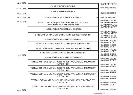 The LPC2148 memory map incorporates several distinct regions, as shown in Fig 4.2 In addition, the CPU interrupt vectors may be remapped to allow them to reside in either flash memory (the default) or on-chip static RAM.
Fig.3(m):Memorymap
The LPC2148 memory map incorporates several distinct regions, as shown in Fig 4.2 In addition, the CPU interrupt vectors may be remapped to allow them to reside in either flash memory (the default) or on-chip static RAM.
Fig.3(m):Memorymap
The LPC2148 memory map incorporates several distinct regions, as shown in Fig 4.2 In addition, the CPU interrupt vectors may be remapped to allow them to reside in either flash memory (the default) or on-chip static RAM.
Fig.3(m):Memorymap
3.7.4 Interrupt Controller
The Vectored Interrupt Controller (VIC) accepts all of the interrupt request inputs and categorizes them as Fast Interrupt Request (FIQ), vectored Interrupt Request (IRQ), and non-vectored IRQ as defined by programmable settings. The programmable assignment scheme means that priorities of interrupts from the various peripherals can be dynamically assigned and adjusted. Fast interrupt request (FIQ) has the highest priority. If more than one request is assigned to FIQ, the VIC combines the requests to produce the FIQ signal to the ARM processor. The fastest possible FIQ latency is achieved when only one request is classified as FIQ, because then the FIQ service routine does not need to branch into the interrupt service routine but can run from the interrupt vector location. If more than one request is assigned to the FIQ class, the FIQ service routine will read a word from the VIC that identifies which FIQ source(s) is (are) requesting an interrupt. Vectored IRQs have the middle priority. Sixteen of the interrupt requests can be assigned to this category. Any of the interrupt requests can be assigned to any of the 16 vectored IRQ slots, among which slot 0 has the highest priority and slot 15 has the lowest. Non-vectored IRQs have the lowest priority. The VIC combines the requests from all the vectored and non-vectored IRQs to produce the IRQ signal to the ARM processor. The IRQ service routine can start by reading a register from the VIC and jumping there. If any of the vectored IRQs are pending, the VIC provides the address of the highest-priority requesting IRQs service routine, otherwise it provides the address of a default routine that is shared by all the non-vectored IRQs. The default routine can read another VIC register to see what IRQs are active.
- Interrupt Sources
3.8.4 REAL MONITOR
Real Monitor is a configurable software module, developed by ARM Inc., which enables real-time debug. It is a lightweight debug monitor that runs in the background while users debug their foreground application. It communicates with the host using the DCC, which is present in the Embedded ICE logic. The LPC2148 contain a specific configuration of Real Monitor software programmed into the on-chip flash memory.
ARM7 LPC2148 is ARM7 TDMI-S Core Board Microcontroller that uses 16/32-Bit 64 Pin (LQFP) Microcontroller no. LPC2148 from Philips (NXP). All resources inside LPC2148 is quite perfect, so it is the most suitable to learn and study because if user can learn and understand the applications of all resources inside MCU well, it makes user can modify, apply and develop many excellent applications in the future. Because Hardware system of LPC2148 includes the necessary devices within only one MCU such as USB, ADC, DAC, Timer/Counter, PWM, Capture, I2C, SPI, UART, and etc.
Features of Board
Use 16/32 Bit ARM7 TDMI-S MCU No. LPC2148 from Philips (NXP).Has 512 KB Flash Memory and 40KB Static RAM internal MCU.Use 12.00MHz Crystal, so MCU can process data with the maximum high speed at 60MHz when using it with Phase-Locked Loop (PLL) internal MCU.Has RTC Circuit (Real Time Clock) with 32.768 KHz XTAL and Battery Backup.Support In-System Programming (ISP) and In-Application Programming (IAP) through On-Chip Boot-Loader Software via Port UART-0 (RS232).
Has circuit to connect with standard 20 Pin JTAG ARM for Real Time Debugging 7-12V AC/DC Power Supply.Has standard 2.0 USB as Full Speed inside (USB Function has 32 End Point).Has Circuit to connect with Dot-Matrix LCD with circuit to adjust its contrast by using 16 PIN Connector.Has RS232 Communication Circuit by using 2 Channel.Has SD/MMC card connector circuit by using SSP.Has EEPROM interface using I2C.Has PS2 keyboard interface.All port pins are extracted externally for further interfaces.
3.8.5 Pulse Width Modulation (PWM)
Pulse-width modulation (PWM) is a commonly used technique for controlling power to an electrical device, made practical by modern electronic power switches. The average value of voltage (and current) fed to the load is controlled by turning the switch between supply and load on and off at a fast pace. The longer the switch is on compared to the off periods, the higher the power supplied to the load is.
The PWM switching frequency has to be much faster than what would affect the load, which is to say the device that uses the power. Typically switchings have to be done several times a minute in an electric stove, 120 Hz in a lamp dimmer, from few kilohertz (kHz) to tens of kHz for a motor drive and well into the tens or hundreds of kHz in audio amplifiers and computer power supplies.
The term duty cycle describes the proportion of on time to the regular interval or period of time; a low duty cycle corresponds to low power, because the power is off for most of the time. Duty cycle is expressed in percent, 100% being fully on.
The main advantage of PWM is that power loss in the switching devices is very low. When a switch is off there is practically no current, and when it is on, there is almost no voltage drop across the switch. Power loss, being the product of voltage
and current, is thus in both cases close to zero. PWM works also well with digital controls, which, because of their on/off nature, can easily set the needed duty cycle. PWM has also been used in certain communication systems where its duty cycle has been used to convey information over a communications channel.
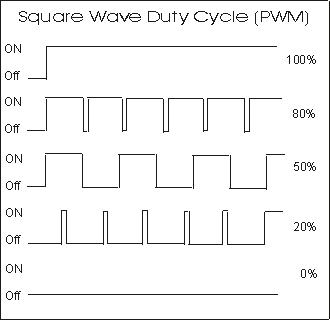 Fig. 3.(n):Duty Cycles of PWM
3.8.6 Power Delivery
PWM can be used to adjust the total amount of power delivered to a load without losses normally incurred when a power transfer is limited by resistive means. The drawbacks are the pulsations defined by the duty cycle, switching frequency and properties of the load. With a sufficiently high switching frequency and, when necessary, using additional passive electronic filters the pulse train can be smoothed and average analog waveform recovered.
High frequency PWM power control systems are easily realisable with semiconductor switches. As has been already stated above almost no power is dissipated by the switch in either on or off state. However, during the transitions between on and off states both voltage and current are non-zero and thus considerable power is dissipated in the switches. Luckily, the change of state between fully on and fully off is quite rapid (typically less than 100 nanoseconds) relative to typical on or
off times, and so the average power dissipation is quite low compared to the power being delivered even when high switching frequencies are used.
Modern semiconductor switches such as MOSFETs or Insulated-gate bipolar transistors (IGBTs) are quite ideal components. Thus high efficiency controllers can be built. Typically frequency converters used to control AC motors have efficiency that is better than 98 %. Switching power supplies have lower efficiency due to low output voltage levels (often even less than 2 V for microprocessors are needed) but still more than 70-80 % efficiency can be achieved. Variable-speed fan controllers for computers usually use PWM, as it is far more efficient when compared to a potentiometer or rheostat. (Neither of the latter is practical to operate electronically; they would require a small drive motor).
Light dimmers for home use employ a specific type of PWM control. Home use light dimmers typically include electronic circuitry which suppresses current flow during defined portions of each cycle of the AC line voltage. Adjusting the brightness of light emitted by a light source is then merely a matter of setting at what voltage (or phase) in the AC half cycle the dimmer begins to provide electrical current to the light source. In this case the PWM duty cycle is the ratio of the conduction time to the duration of the half AC cycle defined by the frequency of the AC line voltage.
3.8.7 Pulse Width Modulation (PWM) in ARM LPC2148
The PWM is based on the standard Timer block and inherits all of its features, although only the PWM function is pinned out on the LPC2141/2/4/6/8. The Timer is designed to count cycles of the peripheral clock (PCLK) and optionally generate interrupts or perform other actions when specified timer values occur, based on seven match registers. It also includes four capture inputs to save the timer value when an input signal transitions, and optionally generate an interrupt when those events occur. The PWM function is in addition to these features, and is based on match register events.The ability to separately control rising and falling edge locations allows the PWM to be used for more applications. For instance, multi-phase motor control typically requires three non-overlapping PWM outputs with individual control of all three pulse widths and positions.
Two match registers can be used to provide a single edge controlled PWM output. One match register (PWMMR0) controls the PWM cycle rate, by resetting the
count upon match. The other match register controls the PWM edge position. Additional single edge controlled PWM outputs require only one match register each, since the repetition rate is the same for all PWM outputs. Multiple single edge controlled PWM outputs will all have a rising edge at the beginning of each PWM cycle, when an PWMMR0 match occurs.
Three match registers can be used to provide a PWM output with both edges controlled. Again, the PWMMR0 match register controls the PWM cycle rate. The other match registers control the two PWM edge positions. Additional double edge controlled PWM outputs require only two match registers each, since the repetition rate is the same for all PWM outputs.
With double edge controlled PWM outputs, specific match registers control the rising and falling edge of the output. This allows both positive going PWM pulses (when the rising edge occurs prior to the falling edge), and negative going PWM pulses (when the falling edge occurs prior to the rising edge).
Fig. 3.(n):Duty Cycles of PWM
3.8.6 Power Delivery
PWM can be used to adjust the total amount of power delivered to a load without losses normally incurred when a power transfer is limited by resistive means. The drawbacks are the pulsations defined by the duty cycle, switching frequency and properties of the load. With a sufficiently high switching frequency and, when necessary, using additional passive electronic filters the pulse train can be smoothed and average analog waveform recovered.
High frequency PWM power control systems are easily realisable with semiconductor switches. As has been already stated above almost no power is dissipated by the switch in either on or off state. However, during the transitions between on and off states both voltage and current are non-zero and thus considerable power is dissipated in the switches. Luckily, the change of state between fully on and fully off is quite rapid (typically less than 100 nanoseconds) relative to typical on or
off times, and so the average power dissipation is quite low compared to the power being delivered even when high switching frequencies are used.
Modern semiconductor switches such as MOSFETs or Insulated-gate bipolar transistors (IGBTs) are quite ideal components. Thus high efficiency controllers can be built. Typically frequency converters used to control AC motors have efficiency that is better than 98 %. Switching power supplies have lower efficiency due to low output voltage levels (often even less than 2 V for microprocessors are needed) but still more than 70-80 % efficiency can be achieved. Variable-speed fan controllers for computers usually use PWM, as it is far more efficient when compared to a potentiometer or rheostat. (Neither of the latter is practical to operate electronically; they would require a small drive motor).
Light dimmers for home use employ a specific type of PWM control. Home use light dimmers typically include electronic circuitry which suppresses current flow during defined portions of each cycle of the AC line voltage. Adjusting the brightness of light emitted by a light source is then merely a matter of setting at what voltage (or phase) in the AC half cycle the dimmer begins to provide electrical current to the light source. In this case the PWM duty cycle is the ratio of the conduction time to the duration of the half AC cycle defined by the frequency of the AC line voltage.
3.8.7 Pulse Width Modulation (PWM) in ARM LPC2148
The PWM is based on the standard Timer block and inherits all of its features, although only the PWM function is pinned out on the LPC2141/2/4/6/8. The Timer is designed to count cycles of the peripheral clock (PCLK) and optionally generate interrupts or perform other actions when specified timer values occur, based on seven match registers. It also includes four capture inputs to save the timer value when an input signal transitions, and optionally generate an interrupt when those events occur. The PWM function is in addition to these features, and is based on match register events.The ability to separately control rising and falling edge locations allows the PWM to be used for more applications. For instance, multi-phase motor control typically requires three non-overlapping PWM outputs with individual control of all three pulse widths and positions.
Two match registers can be used to provide a single edge controlled PWM output. One match register (PWMMR0) controls the PWM cycle rate, by resetting the
count upon match. The other match register controls the PWM edge position. Additional single edge controlled PWM outputs require only one match register each, since the repetition rate is the same for all PWM outputs. Multiple single edge controlled PWM outputs will all have a rising edge at the beginning of each PWM cycle, when an PWMMR0 match occurs.
Three match registers can be used to provide a PWM output with both edges controlled. Again, the PWMMR0 match register controls the PWM cycle rate. The other match registers control the two PWM edge positions. Additional double edge controlled PWM outputs require only two match registers each, since the repetition rate is the same for all PWM outputs.
With double edge controlled PWM outputs, specific match registers control the rising and falling edge of the output. This allows both positive going PWM pulses (when the rising edge occurs prior to the falling edge), and negative going PWM pulses (when the falling edge occurs prior to the rising edge).
 3.9 GLOBAL POSITIONING SYSTEM(GPS)
The Global Positioning System (GPS) is the only fully functional Global Navigation Satellite System (GNSS). The GPS uses a constellation of between 24 and 32 Medium Earth Orbit satellites that transmit precise microwave signals, which enable GPS receivers to determine their location, speed,. GPS was developed by the United States Department of Defense. Its official name is NAVSTAR-GPS. Although NAVSTAR-GPS is not an acronym, a few backronyms have been created for it. The GPS satellite constellation is managed by the United States Air Force 50th Space Wing.
Global Positioning System is an earth-orbiting-satellite based system that provides signals available anywhere on or above the earth, twenty-four hours a day, which can be used to determine precise time and the position of a GPS receiver in three dimensions. GPS is increasingly used as an input for Geographic Information Systems particularly for precise positioning of geospatial data and the collection of data in the field.Precise positioning is possible using GPS receivers at reference locations providing corrections and relative positioning data for remote receivers. Time and frequency dissemination, based on the precise clocks on board the SVs and controlled by the monitor stations, is another, use for GPS. Astronomical observatories telecommunications facilities and laboratory standards can be set to precise time signals or controlled to accurate frequencies by special purpose GPS receivers.
Similar satellite navigation systems include the Russian GLONASS (incomplete as of 2008), the upcoming European Galileo positioning system, the proposed COMPASS navigation system of China, and IRNSS of India.
Following the shooting down of Korean Air Lines Flight 007 in 1983, President Ronald Reagan issued a directive making the system available free for civilian use as a common good. Since then, GPS has become a widely used aid to navigation worldwide, and a useful tool for map-making, land surveying, commerce, scientific uses, and hobbies such as geocaching. GPS also provides a precise time reference used in many applications including scientific study of earthquakes, and synchronization of telecommunications networks.
3.9 GLOBAL POSITIONING SYSTEM(GPS)
The Global Positioning System (GPS) is the only fully functional Global Navigation Satellite System (GNSS). The GPS uses a constellation of between 24 and 32 Medium Earth Orbit satellites that transmit precise microwave signals, which enable GPS receivers to determine their location, speed,. GPS was developed by the United States Department of Defense. Its official name is NAVSTAR-GPS. Although NAVSTAR-GPS is not an acronym, a few backronyms have been created for it. The GPS satellite constellation is managed by the United States Air Force 50th Space Wing.
Global Positioning System is an earth-orbiting-satellite based system that provides signals available anywhere on or above the earth, twenty-four hours a day, which can be used to determine precise time and the position of a GPS receiver in three dimensions. GPS is increasingly used as an input for Geographic Information Systems particularly for precise positioning of geospatial data and the collection of data in the field.Precise positioning is possible using GPS receivers at reference locations providing corrections and relative positioning data for remote receivers. Time and frequency dissemination, based on the precise clocks on board the SVs and controlled by the monitor stations, is another, use for GPS. Astronomical observatories telecommunications facilities and laboratory standards can be set to precise time signals or controlled to accurate frequencies by special purpose GPS receivers.
Similar satellite navigation systems include the Russian GLONASS (incomplete as of 2008), the upcoming European Galileo positioning system, the proposed COMPASS navigation system of China, and IRNSS of India.
Following the shooting down of Korean Air Lines Flight 007 in 1983, President Ronald Reagan issued a directive making the system available free for civilian use as a common good. Since then, GPS has become a widely used aid to navigation worldwide, and a useful tool for map-making, land surveying, commerce, scientific uses, and hobbies such as geocaching. GPS also provides a precise time reference used in many applications including scientific study of earthquakes, and synchronization of telecommunications networks.

 Fig 3(o) GPS satellite
![\left [x_i, y_i, z_i, t_i\right ]](https://images.ukdissertations.com/18/0025970.029.jpg) where the subscript i denotes the satellite number and has the value 1, 2, 3, or 4. Knowing the indicated time the message was received
where the subscript i denotes the satellite number and has the value 1, 2, 3, or 4. Knowing the indicated time the message was received  , the GPS receiver can compute the indicated transit time,
  . of the message.
Assuming the message traveled at the speed of light, c, the distance travelled,
. of the message.
Assuming the message traveled at the speed of light, c, the distance travelled,  can be computed as
  . Knowing the distance from GPS receiver to a satellite and the position of a satellite implies that the GPS receiver is on the surface of a sphere centered at the position of a satellite. Thus we know that the indicated position of the GPS receiver is at or near the intersection of the surfaces of four spheres. In the ideal case of no errors, the GPS receiver will be at an intersection of the surfaces of four spheres. The surfaces of two spheres if they intersect in more than one point intersect in a circle. A figure, two sphere surfaces intersecting in a circle, is shown below.
 Two Sphere Surfaces Intersecting in a Circle
The article, trilateration, shows mathematically that two spheres intersecting in more than one point intersect in a circle.
Two Sphere Surfaces Intersecting in a Circle
The article, trilateration, shows mathematically that two spheres intersecting in more than one point intersect in a circle.
 Surface of Sphere Intersecting a Circle (not disk) at Two Points
A circle and sphere surface in most cases of practical interest intersects at two points, although it is conceivable that they could intersect in 0 or 1 point. Another figure, Surface of Sphere Intersecting a Circle (not disk) at Two Points, is shown to aid in visualizing this intersection. Again trilateration clearly show this mathematically. The correct position of the GPS receiver is the one that is closest to the fourth sphere.
Surface of Sphere Intersecting a Circle (not disk) at Two Points
A circle and sphere surface in most cases of practical interest intersects at two points, although it is conceivable that they could intersect in 0 or 1 point. Another figure, Surface of Sphere Intersecting a Circle (not disk) at Two Points, is shown to aid in visualizing this intersection. Again trilateration clearly show this mathematically. The correct position of the GPS receiver is the one that is closest to the fourth sphere.
 denote the distance from the valid estimate of GPS receiver position to the fourth satellite and let
  denote the pseudo range of the fourth satellite. Let
  . Note that
  is the distance from the computed GPS receiver position to the surface of the sphere corresponding to the fourth satellite. Thus the quotient,
  , provides an estimate of:
(correct time) - (time indicated by the receiver's on-board clock)
and the GPS receiver clock can be advanced if
, provides an estimate of:
(correct time) - (time indicated by the receiver's on-board clock)
and the GPS receiver clock can be advanced if  is positive or delayed if is negative.
 Fig 3(p) GPS Constellation
A visual example of the GPS constellation in motion with the Earth rotating. Notice how the number of satellites in view from a given point on the Earth's surface, in this example at 45°N, changes with time.
The space segment (SS) comprises the orbiting GPS satellites, or Space Vehicles (SV) in GPS parlance. The GPS design originally called for 24 SVs, eight each in three circular orbital planes, but this was modified to six planes with four satellites each. The orbital
Fig 3(p) GPS Constellation
A visual example of the GPS constellation in motion with the Earth rotating. Notice how the number of satellites in view from a given point on the Earth's surface, in this example at 45°N, changes with time.
The space segment (SS) comprises the orbiting GPS satellites, or Space Vehicles (SV) in GPS parlance. The GPS design originally called for 24 SVs, eight each in three circular orbital planes, but this was modified to six planes with four satellites each. The orbital
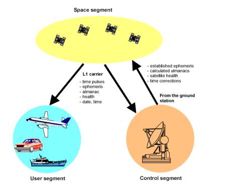
 Figure 3(q): A GPS satellite
planes are centered on the Earth, not rotating with respect to the distant stars. The six planes have approximately 55° inclination (tilt relative to Earth's equator) and are separated by 60° right ascension of the ascending node (angle along the equator from a reference point to the orbit's intersection). The orbits are arranged so that at least six satellites are always within line of sight from almost everywhere on Earth's surface.
Orbiting at an altitude of approximately 20,200 kilometers (12,600 miles or 10,900 nautical miles; orbital radius of 26,600 km (16,500 mi or 14,400 NM)), each SV makes two complete orbits each sidereal day. The ground track of each satellite therefore repeats each (sidereal) day. This was very helpful during development, since even with just four satellites, correct alignment means all four are visible from one spot for a few hours each day. For military operations, the ground track repeat can be used to ensure good coverage in combat zones.
As of March 2008, there are 31 actively broadcasting satellites in the GPS constellation. The additional satellites improve the precision of GPS receiver calculations by providing redundant measurements. With the increased number of satellites, the constellation was changed to a nonuniform arrangement. Such an arrangement was shown to improve reliability and availability of the system, relative to a uniform system, when multiple satellites fail.
Some reports in 2008 indicated that the 32nd satellite was causing difficulties for some GPS receivers.
Figure 3(q): A GPS satellite
planes are centered on the Earth, not rotating with respect to the distant stars. The six planes have approximately 55° inclination (tilt relative to Earth's equator) and are separated by 60° right ascension of the ascending node (angle along the equator from a reference point to the orbit's intersection). The orbits are arranged so that at least six satellites are always within line of sight from almost everywhere on Earth's surface.
Orbiting at an altitude of approximately 20,200 kilometers (12,600 miles or 10,900 nautical miles; orbital radius of 26,600 km (16,500 mi or 14,400 NM)), each SV makes two complete orbits each sidereal day. The ground track of each satellite therefore repeats each (sidereal) day. This was very helpful during development, since even with just four satellites, correct alignment means all four are visible from one spot for a few hours each day. For military operations, the ground track repeat can be used to ensure good coverage in combat zones.
As of March 2008, there are 31 actively broadcasting satellites in the GPS constellation. The additional satellites improve the precision of GPS receiver calculations by providing redundant measurements. With the increased number of satellites, the constellation was changed to a nonuniform arrangement. Such an arrangement was shown to improve reliability and availability of the system, relative to a uniform system, when multiple satellites fail.
Some reports in 2008 indicated that the 32nd satellite was causing difficulties for some GPS receivers.
 A typical OEM GPS receiver module measuring 15×17 mm.
GPS receivers may include an input for differential corrections, using the RTCM SC-104 format. This is typically in the form of a RS-232 port at 4,800 bit/s speed. Data is actually sent at a much lower rate, which limits the accuracy of the signal sent using RTCM. Receivers with internal DGPS receivers can outperform those using external RTCM data. As of 2006, even low-cost units commonly include Wide Area Augmentation System (WAAS) receivers.
A typical OEM GPS receiver module measuring 15×17 mm.
GPS receivers may include an input for differential corrections, using the RTCM SC-104 format. This is typically in the form of a RS-232 port at 4,800 bit/s speed. Data is actually sent at a much lower rate, which limits the accuracy of the signal sent using RTCM. Receivers with internal DGPS receivers can outperform those using external RTCM data. As of 2006, even low-cost units commonly include Wide Area Augmentation System (WAAS) receivers.
 Fig 3(r)A typical GPS receiver with integrated antenna.
Many GPS receivers can relay position data to a PC or other device using the NMEA 0183 protocol, or the newer and less widely used NMEA 2000. Although these protocols are officially defined by the NMEA, references to the these protocols have been compiled from public records, allowing open source tools like gpsd to read the protocol without violating intellectual property laws. Other proprietary protocols exist as well, such as the SiRF and MTK protocols. Receivers can interface with other devices using methods including a serial connection, USB or Bluetooth.
Fig 3(r)A typical GPS receiver with integrated antenna.
Many GPS receivers can relay position data to a PC or other device using the NMEA 0183 protocol, or the newer and less widely used NMEA 2000. Although these protocols are officially defined by the NMEA, references to the these protocols have been compiled from public records, allowing open source tools like gpsd to read the protocol without violating intellectual property laws. Other proprietary protocols exist as well, such as the SiRF and MTK protocols. Receivers can interface with other devices using methods including a serial connection, USB or Bluetooth.
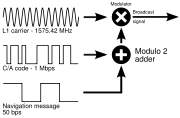 Fig 3(s)GPS broadcast signal
Each GPS satellite continuously broadcasts a Navigation Message at 50 bit/s giving the time-of-week, GPS week number and satellite health information (all transmitted in the first part of the message), an ephemeris (transmitted in the second part of the message) and an almanac (later part of the message). The messages are sent in frames, each taking 30 seconds to transmit 1500 bits.
The first 6 seconds of every frame contains data describing the satellite clock and its relationship to GPS time. The next 12 seconds contain the ephemeris data, giving the satellite's own precise orbit. The ephemeris is updated every 2 hours and is generally valid for 4 hours, with provisions for updates every 6 hours or longer in non-nominal conditions. The time needed to acquire the ephemeris is becoming a significant element of the delay to first position fix, because, as the hardware becomes more capable, the time to lock onto the satellite signals shrinks, but the ephemeris data requires 30 seconds (worst case) before it is received, due to the low data transmission rate.
The almanac consists of coarse orbit and status information for each satellite in the constellation, an ionosphere model, and information to relate GPS derived time to Coordinated Universal Time (UTC). A new part of the almanac is received for the last 12 seconds in each 30 second frame. Each frame contains 1/25th of the almanac, so 12.5 minutes are required to receive the entire almanac from a single satellite. The almanac serves several purposes. The first is to assist in the acquisition of satellites at power-up by allowing the receiver to generate a list of visible satellites based on stored position and time, while an ephemeris from each satellite is needed to compute position fixes using that satellite. In older hardware, lack of an almanac in a new receiver would cause long delays before providing a valid position, because the search for each satellite was a slow process. Advances in hardware have made the acquisition process much faster, so not having an almanac is no longer an issue. The second purpose is for relating time derived from the GPS (called GPS time) to the international time standard of UTC. Finally, the almanac allows a single frequency receiver to correct for ionospheric error by using a global ionospheric model. The corrections are not as accurate as augmentation systems like WAAS or dual frequency receivers. However it is often better than no correction since ionospheric error is the largest error source for a single frequency GPS receiver. An important thing to note about navigation data is that each satellite transmits only its own ephemeris, but transmits an almanac for all satellites.
Each satellite transmits its navigation message with at least two distinct spread spectrum codes: the Coarse / Acquisition (C/A) code, which is freely available to the public, and the Precise (P) code, which is usually encrypted and reserved for military applications. The C/A code is a 1023 length Gold code at 1.023 million chips per second so that it repeats every millisecond. As pointed out in a chip is essentially the same thing as a bit and chips per second are the same as bits per second. The justification for coming up with this new term, chip, is that in some cases a sequence of bits is used as a type of Modulation and contains no information.
Each satellite has its own C/A code so that it can be uniquely identified and received separately from the other satellites transmitting on the same frequency. The P-code is a 10.23 mega chip per second PRN code that repeats only every week. When the "anti-spoofing" mode is on, as it is in normal operation, the P code is encrypted by the Y-code to produce the P(Y) code, which can only be decrypted by units with a valid decryption key. Both the C/A and P(Y) codes impart the precise time-of-day to the user.
where the subscript i denotes which satellite and has the value 1, 2, 3, or 4. Knowing the indicated time the message was received, the GPS receiver can compute the indicated transit time, . of the message. Assuming the message traveled at the speed of light, c, the distance traveled, can be computed as . Knowing the distance from GPS receiver to a satellite and the position of a satellite implies that the GPS receiver is on the surface of a sphere centered at the position of a satellite. Thus we know that the indicated position of the GPS receiver is at or near the intersection of the surfaces of four spheres. In the ideal case of no errors, the GPS receiver will be at an intersection of the surfaces of four spheres. The surfaces of two spheres if they intersect in more than one point intersect in a circle. A figure, Two Sphere Surfaces Intersecting in a Circle, is shown below depicting this which hopefully will aid the reader in visualizing this intersection.
Fig 3(s)GPS broadcast signal
Each GPS satellite continuously broadcasts a Navigation Message at 50 bit/s giving the time-of-week, GPS week number and satellite health information (all transmitted in the first part of the message), an ephemeris (transmitted in the second part of the message) and an almanac (later part of the message). The messages are sent in frames, each taking 30 seconds to transmit 1500 bits.
The first 6 seconds of every frame contains data describing the satellite clock and its relationship to GPS time. The next 12 seconds contain the ephemeris data, giving the satellite's own precise orbit. The ephemeris is updated every 2 hours and is generally valid for 4 hours, with provisions for updates every 6 hours or longer in non-nominal conditions. The time needed to acquire the ephemeris is becoming a significant element of the delay to first position fix, because, as the hardware becomes more capable, the time to lock onto the satellite signals shrinks, but the ephemeris data requires 30 seconds (worst case) before it is received, due to the low data transmission rate.
The almanac consists of coarse orbit and status information for each satellite in the constellation, an ionosphere model, and information to relate GPS derived time to Coordinated Universal Time (UTC). A new part of the almanac is received for the last 12 seconds in each 30 second frame. Each frame contains 1/25th of the almanac, so 12.5 minutes are required to receive the entire almanac from a single satellite. The almanac serves several purposes. The first is to assist in the acquisition of satellites at power-up by allowing the receiver to generate a list of visible satellites based on stored position and time, while an ephemeris from each satellite is needed to compute position fixes using that satellite. In older hardware, lack of an almanac in a new receiver would cause long delays before providing a valid position, because the search for each satellite was a slow process. Advances in hardware have made the acquisition process much faster, so not having an almanac is no longer an issue. The second purpose is for relating time derived from the GPS (called GPS time) to the international time standard of UTC. Finally, the almanac allows a single frequency receiver to correct for ionospheric error by using a global ionospheric model. The corrections are not as accurate as augmentation systems like WAAS or dual frequency receivers. However it is often better than no correction since ionospheric error is the largest error source for a single frequency GPS receiver. An important thing to note about navigation data is that each satellite transmits only its own ephemeris, but transmits an almanac for all satellites.
Each satellite transmits its navigation message with at least two distinct spread spectrum codes: the Coarse / Acquisition (C/A) code, which is freely available to the public, and the Precise (P) code, which is usually encrypted and reserved for military applications. The C/A code is a 1023 length Gold code at 1.023 million chips per second so that it repeats every millisecond. As pointed out in a chip is essentially the same thing as a bit and chips per second are the same as bits per second. The justification for coming up with this new term, chip, is that in some cases a sequence of bits is used as a type of Modulation and contains no information.
Each satellite has its own C/A code so that it can be uniquely identified and received separately from the other satellites transmitting on the same frequency. The P-code is a 10.23 mega chip per second PRN code that repeats only every week. When the "anti-spoofing" mode is on, as it is in normal operation, the P code is encrypted by the Y-code to produce the P(Y) code, which can only be decrypted by units with a valid decryption key. Both the C/A and P(Y) codes impart the precise time-of-day to the user.
where the subscript i denotes which satellite and has the value 1, 2, 3, or 4. Knowing the indicated time the message was received, the GPS receiver can compute the indicated transit time, . of the message. Assuming the message traveled at the speed of light, c, the distance traveled, can be computed as . Knowing the distance from GPS receiver to a satellite and the position of a satellite implies that the GPS receiver is on the surface of a sphere centered at the position of a satellite. Thus we know that the indicated position of the GPS receiver is at or near the intersection of the surfaces of four spheres. In the ideal case of no errors, the GPS receiver will be at an intersection of the surfaces of four spheres. The surfaces of two spheres if they intersect in more than one point intersect in a circle. A figure, Two Sphere Surfaces Intersecting in a Circle, is shown below depicting this which hopefully will aid the reader in visualizing this intersection.
 Two Sphere Surfaces Intersecting in a Circle
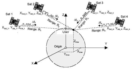 Three dimensional co-ordinate system
 Fig 3(t) 3 Dimensional GPS System
The article, trilateration, shows mathematically how the equation for a circle is determined. A circle and sphere surface in most cases of practical interest intersects at two points, although it is conceivable that they could intersect in 0 or 1 point. Another figure, Surface of Sphere Intersecting a Circle (not disk) at Two Points, is shown below to aid in visualizing this intersection. Again trilateration clearly show this mathematically. The correct position of the GPS receiver is the one that is closest to the fourth sphere. This paragraph has described the basic concept of GPS while ignoring errors. The next problem is how to process the messages when errors are present.
Fig 3(t) 3 Dimensional GPS System
The article, trilateration, shows mathematically how the equation for a circle is determined. A circle and sphere surface in most cases of practical interest intersects at two points, although it is conceivable that they could intersect in 0 or 1 point. Another figure, Surface of Sphere Intersecting a Circle (not disk) at Two Points, is shown below to aid in visualizing this intersection. Again trilateration clearly show this mathematically. The correct position of the GPS receiver is the one that is closest to the fourth sphere. This paragraph has described the basic concept of GPS while ignoring errors. The next problem is how to process the messages when errors are present.
 Surface of Sphere Intersecting a Circle (not disk) at Two Points
Let denote the clock error or bias, the amount by which the receiver's clock is slow. The GPS receiver has four unknowns, the three components of GPS receiver position and the clock bias
Surface of Sphere Intersecting a Circle (not disk) at Two Points
Let denote the clock error or bias, the amount by which the receiver's clock is slow. The GPS receiver has four unknowns, the three components of GPS receiver position and the clock bias ![\left [x, y, z, b\right ]](https://images.ukdissertations.com/18/0025970.052.jpg) . The equation of the sphere surfaces are given by:
. The equation of the sphere surfaces are given by:
 Another useful form of these equations is in terms of the pseudoranges, which are simply the ranges approximated based on GPS receiver clock's indicated (i.e. uncorrected) time so that
  . Then the equations becomes:
 .
Two of the most important methods of computing GPS receiver position and clock bias are (1) trilateration followed by one dimensional numerical root finding and (2) multidimensional Newton-Raphson. These two methods along with their advantages are discussed.
solve by trilateration followed by one dimensional numerical root finding. This method involves using Trilateration to determine the intersection of the surfaces of three spheres. It is clearly shown in trilateration that the surfaces of three spheres intersect in 0, 1, or 2 points. In the usual case of two intersections, the solution which is nearest the surface of the sphere corresponding to the fourth satellite is chosen. The surface of the earth can also sometimes be used instead, especially in the case of civilian GPS receivers since it is illegal in the United States to track vehicles of more than 60,000 feet in altitude. The bias,is then computed based on the distance from the solution to the surface of the sphere corresponding to the fourth satellite. Using an updated received time based on this bias, new spheres are computed and the process is repeated. One advantage of this method is that it involves one dimensional as opposed to multidimensional numerical root finding.
Utilize multidimensional Newton-Raphson. Linearize around an approximate solution say
.
Two of the most important methods of computing GPS receiver position and clock bias are (1) trilateration followed by one dimensional numerical root finding and (2) multidimensional Newton-Raphson. These two methods along with their advantages are discussed.
solve by trilateration followed by one dimensional numerical root finding. This method involves using Trilateration to determine the intersection of the surfaces of three spheres. It is clearly shown in trilateration that the surfaces of three spheres intersect in 0, 1, or 2 points. In the usual case of two intersections, the solution which is nearest the surface of the sphere corresponding to the fourth satellite is chosen. The surface of the earth can also sometimes be used instead, especially in the case of civilian GPS receivers since it is illegal in the United States to track vehicles of more than 60,000 feet in altitude. The bias,is then computed based on the distance from the solution to the surface of the sphere corresponding to the fourth satellite. Using an updated received time based on this bias, new spheres are computed and the process is repeated. One advantage of this method is that it involves one dimensional as opposed to multidimensional numerical root finding.
Utilize multidimensional Newton-Raphson. Linearize around an approximate solution say ![\left [x^{(k)}, y^{(k)}, z^{(k)}, b^{(k)}\right ]](https://images.ukdissertations.com/18/0025970.056.jpg) from iteration k, then solve four linear equations derived from the quadratic equations above to obtain
from iteration k, then solve four linear equations derived from the quadratic equations above to obtain ![\left [x^{(k+1)}, y^{(k+1)}, z^{(k+1)}, b^{(k+1)}\right ]](https://images.ukdissertations.com/18/0025970.057.jpg) . The radii are large and so the sphere surfaces are close to flat. This near flatness may cause the iterative procedure to converge rapidly in the case where is near the correct value and the primary change is in the values of
. The radii are large and so the sphere surfaces are close to flat. This near flatness may cause the iterative procedure to converge rapidly in the case where is near the correct value and the primary change is in the values of  , since in this case the problem is merely to find the intersection of nearly flat surfaces and thus close to a linear problem. However when is changing significantly, this near flatness does not appear to be advantageous in producing rapid convergence, since in this case these near flat surfaces will be moving as the spheres expand and contract. This possible fast convergence is an advantage of this method. Also it has been claimed that this method is the "typical" method used by GPS receivers. A disadvantage of this method is that according to, "There are no good general methods for solving systems of more than one nonlinear equation."
Other methods include: Solve for the intersection of the expanding signals form light cones in 4-space cones, Solve for the intersection of hyperboloids determined by the time difference of signals received from satellites utilizing multilateration, Solve the equations in accordance with.
More than four satellites should be used, if available. This results in an over-determined system of equations with no unique solution, which must be solved by least-squares or a similar technique. If all visible satellites are used, the results are always at least as good as using the four best, and usually better. Also the errors in results can be estimated through the residuals. With each combination of four or more satellites, a geometric dilution of precision (GDOP) vector can be calculated, based on the relative sky positions of the satellites used. As more satellites are picked up, pseudoranges from more combinations of four satellites can be processed to add more estimates to the location and clock offset. The receiver then determines which combinations to use and how to calculate the estimated position by determining the weighted average of these positions and clock offsets. After the final location and time are calculated, the location is expressed in a specific coordinate system such as latitude and longitude, using the WGS 84 geodetic datum or a local system specific to a country.
Finally, results from other positioning systems such as GLONASS or the upcoming Galileo can be used in the fit, or used to double check the result. (By design, these systems use the same bands; so much of the receiver circuitry can be shared, though the decoding is different.
3.10 GSM (Global System for Mobile communications)
GSM (Global System for Mobile communications) is a cellular network, which means that mobile phones connect to it by searching for cells in the immediate vicinity. GSM networks operate in four different frequency ranges. Most GSM networks operate in the 900 MHz or 1800 MHz bands. Some countries in the Americas use the 850 MHz and 1900 MHz bands because the 900 and 1800 MHz frequency bands were already allocated.
The rarer 400 and 450 MHz frequency bands are assigned in some countries, where these frequencies were previously used for first-generation systems.
GSM-900 uses 890–915 MHz to send information from the mobile station to the base station (uplink) and 935–960 MHz for the other direction (downlink), providing 124 RF channels (channel numbers 1 to 124) spaced at 200 kHz. Duplex spacing of 45 MHz is used. In some countries the GSM-900 band has been extended to cover a larger frequency range. This 'extended GSM', E-GSM, uses 880–915 MHz (uplink) and 925–960 MHz (downlink), adding 50 channels (channel numbers 975 to 1023 and 0) to the original GSM-900 band. Time division multiplexing is used to allow eight full-rate or sixteen half-rate speech channels per radio frequency channel. There are eight radio timeslots (giving eight burst periods) grouped into what is called a TDMA frame. Half rate channels use alternate frames in the same timeslot. The channel data rate is 270.833 kbit/s, and the frame duration is 4.615 ms.
3.10.1GSM Advantages:
GSM also pioneered a low-cost, to the network carrier, alternative to voice calls, the Short t message service (SMS, also called "text messaging"), which is now supported on other mobile standards as well. Another advantage is that the standard includes one worldwide Emergency telephone number, 112. This makes it easier for international travelers to connect to emergency services without knowing the local emergency number.
3.10.2The GSM Network:
GSM provides recommendations, not requirements. The GSM specifications define the functions and interface requirements in detail but do not address the hardware. The GSM network is divided into three major systems: the switching system (SS), the base station system (BSS), and the operation and support system (OSS).
, since in this case the problem is merely to find the intersection of nearly flat surfaces and thus close to a linear problem. However when is changing significantly, this near flatness does not appear to be advantageous in producing rapid convergence, since in this case these near flat surfaces will be moving as the spheres expand and contract. This possible fast convergence is an advantage of this method. Also it has been claimed that this method is the "typical" method used by GPS receivers. A disadvantage of this method is that according to, "There are no good general methods for solving systems of more than one nonlinear equation."
Other methods include: Solve for the intersection of the expanding signals form light cones in 4-space cones, Solve for the intersection of hyperboloids determined by the time difference of signals received from satellites utilizing multilateration, Solve the equations in accordance with.
More than four satellites should be used, if available. This results in an over-determined system of equations with no unique solution, which must be solved by least-squares or a similar technique. If all visible satellites are used, the results are always at least as good as using the four best, and usually better. Also the errors in results can be estimated through the residuals. With each combination of four or more satellites, a geometric dilution of precision (GDOP) vector can be calculated, based on the relative sky positions of the satellites used. As more satellites are picked up, pseudoranges from more combinations of four satellites can be processed to add more estimates to the location and clock offset. The receiver then determines which combinations to use and how to calculate the estimated position by determining the weighted average of these positions and clock offsets. After the final location and time are calculated, the location is expressed in a specific coordinate system such as latitude and longitude, using the WGS 84 geodetic datum or a local system specific to a country.
Finally, results from other positioning systems such as GLONASS or the upcoming Galileo can be used in the fit, or used to double check the result. (By design, these systems use the same bands; so much of the receiver circuitry can be shared, though the decoding is different.
3.10 GSM (Global System for Mobile communications)
GSM (Global System for Mobile communications) is a cellular network, which means that mobile phones connect to it by searching for cells in the immediate vicinity. GSM networks operate in four different frequency ranges. Most GSM networks operate in the 900 MHz or 1800 MHz bands. Some countries in the Americas use the 850 MHz and 1900 MHz bands because the 900 and 1800 MHz frequency bands were already allocated.
The rarer 400 and 450 MHz frequency bands are assigned in some countries, where these frequencies were previously used for first-generation systems.
GSM-900 uses 890–915 MHz to send information from the mobile station to the base station (uplink) and 935–960 MHz for the other direction (downlink), providing 124 RF channels (channel numbers 1 to 124) spaced at 200 kHz. Duplex spacing of 45 MHz is used. In some countries the GSM-900 band has been extended to cover a larger frequency range. This 'extended GSM', E-GSM, uses 880–915 MHz (uplink) and 925–960 MHz (downlink), adding 50 channels (channel numbers 975 to 1023 and 0) to the original GSM-900 band. Time division multiplexing is used to allow eight full-rate or sixteen half-rate speech channels per radio frequency channel. There are eight radio timeslots (giving eight burst periods) grouped into what is called a TDMA frame. Half rate channels use alternate frames in the same timeslot. The channel data rate is 270.833 kbit/s, and the frame duration is 4.615 ms.
3.10.1GSM Advantages:
GSM also pioneered a low-cost, to the network carrier, alternative to voice calls, the Short t message service (SMS, also called "text messaging"), which is now supported on other mobile standards as well. Another advantage is that the standard includes one worldwide Emergency telephone number, 112. This makes it easier for international travelers to connect to emergency services without knowing the local emergency number.
3.10.2The GSM Network:
GSM provides recommendations, not requirements. The GSM specifications define the functions and interface requirements in detail but do not address the hardware. The GSM network is divided into three major systems: the switching system (SS), the base station system (BSS), and the operation and support system (OSS).
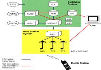 Fig 3(u) GSM Network
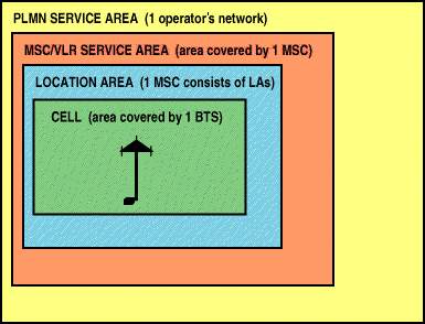 Fig 3(v): GSM Network Area
Location Areas:
The cell is the area given radio coverage by one base transceiver station. The GSM network identifies each cell via the cell global identity (CGI) number assigned to each cell. The location area is a group of cells. It is the area in which the subscriber is paged. Each LA is served by one or more base station controllers, yet only by a single MSC Each LA is assigned a location area identity (LAI) number.
MSC/VLR service areas:
An MSC/VLR service area represents the part of the GSM network that is covered by one MSC and which is reachable, as it is registered in the VLR of the MSC.
PLMN service areas:
The PLMN service area is an area served by one network operator.
3.10.8GSM Specifications:
Specifications for different personal communication services (PCS) systems vary among the different PCS networks. Listed below is a description of the specifications and characteristics for GSM.
Frequency band: The frequency range specified for GSM is 1,850 to 1,990 MHz (mobile station to base station).
Duplex distance: The duplex distance is 80 MHz. Duplex distance is the distance between the uplink and downlink frequencies. A channel has two frequencies, 80 MHz apart.
Channel separation: The separation between adjacent carrier frequencies. In GSM, this is 200 kHz.
Modulation: Modulation is the process of sending a signal by changing the characteristics of a carrier frequency. This is done in GSM via Gaussian minimum shift keying (GMSK).
Transmission rate: GSM is a digital system with an over-the-air bit rate of 270 kbps.
Access method: GSM utilizes the time division multiple access (TDMA) concept. TDMA is a technique in which several different calls may share the same carrier. Each call is assigned a particular time slot.
Speech coder: GSM uses linear predictive coding (LPC). The purpose of LPC is to reduce the bit rate. The LPC provides parameters for a filter that mimics the vocal tract. The signal passes through this filter, leaving behind a residual signal. Speech is encoded at 13 kbps.
3.10.9 GSM Subscriber Services:
Dual-tone multifrequency (DTMF): DTMF is a tone signaling scheme often used for various control purposes via the telephone network, such as remote control of an answering machine. GSM supports full-originating DTMF.
Facsimile group III—GSM supports CCITT Group 3 facsimile. As standard fax machines are designed to be connected to a telephone using analog signals, a special fax converter connected to the exchange is used in the GSM system. This enables a GSM–connected fax to communicate with any analog fax in the network.
Short message services: A convenient facility of the GSM network is the short message service. A message consisting of a maximum of 160 alphanumeric characters can be sent to or from a mobile station. This service can be viewed as an advanced form of alphanumeric paging with a number of advantages. If the subscriber's mobile unit is powered off or has left the coverage area, the message is stored and offered back to the subscriber when the mobile is powered on or has reentered the coverage area of the network. This function ensures that the message will be received.
Cell broadcast: A variation of the short message service is the cell broadcast facility. A message of a maximum of 93 characters can be broadcast to all mobile subscribers in a certain geographic area. Typical applications include traffic congestion warnings and reports on accidents.
Voice mail: This service is actually an answering machine within the network, which is controlled by the subscriber. Calls can be forwarded to the subscriber's voice-mail box and the subscriber checks for messages via a personal security code.
Fax mail: With this service, the subscriber can receive fax messages at any fax machine. The messages are stored in a service center from which they can be retrieved by the subscriber via a personal security code to the desired fax number
Fig 3(v): GSM Network Area
Location Areas:
The cell is the area given radio coverage by one base transceiver station. The GSM network identifies each cell via the cell global identity (CGI) number assigned to each cell. The location area is a group of cells. It is the area in which the subscriber is paged. Each LA is served by one or more base station controllers, yet only by a single MSC Each LA is assigned a location area identity (LAI) number.
MSC/VLR service areas:
An MSC/VLR service area represents the part of the GSM network that is covered by one MSC and which is reachable, as it is registered in the VLR of the MSC.
PLMN service areas:
The PLMN service area is an area served by one network operator.
3.10.8GSM Specifications:
Specifications for different personal communication services (PCS) systems vary among the different PCS networks. Listed below is a description of the specifications and characteristics for GSM.
Frequency band: The frequency range specified for GSM is 1,850 to 1,990 MHz (mobile station to base station).
Duplex distance: The duplex distance is 80 MHz. Duplex distance is the distance between the uplink and downlink frequencies. A channel has two frequencies, 80 MHz apart.
Channel separation: The separation between adjacent carrier frequencies. In GSM, this is 200 kHz.
Modulation: Modulation is the process of sending a signal by changing the characteristics of a carrier frequency. This is done in GSM via Gaussian minimum shift keying (GMSK).
Transmission rate: GSM is a digital system with an over-the-air bit rate of 270 kbps.
Access method: GSM utilizes the time division multiple access (TDMA) concept. TDMA is a technique in which several different calls may share the same carrier. Each call is assigned a particular time slot.
Speech coder: GSM uses linear predictive coding (LPC). The purpose of LPC is to reduce the bit rate. The LPC provides parameters for a filter that mimics the vocal tract. The signal passes through this filter, leaving behind a residual signal. Speech is encoded at 13 kbps.
3.10.9 GSM Subscriber Services:
Dual-tone multifrequency (DTMF): DTMF is a tone signaling scheme often used for various control purposes via the telephone network, such as remote control of an answering machine. GSM supports full-originating DTMF.
Facsimile group III—GSM supports CCITT Group 3 facsimile. As standard fax machines are designed to be connected to a telephone using analog signals, a special fax converter connected to the exchange is used in the GSM system. This enables a GSM–connected fax to communicate with any analog fax in the network.
Short message services: A convenient facility of the GSM network is the short message service. A message consisting of a maximum of 160 alphanumeric characters can be sent to or from a mobile station. This service can be viewed as an advanced form of alphanumeric paging with a number of advantages. If the subscriber's mobile unit is powered off or has left the coverage area, the message is stored and offered back to the subscriber when the mobile is powered on or has reentered the coverage area of the network. This function ensures that the message will be received.
Cell broadcast: A variation of the short message service is the cell broadcast facility. A message of a maximum of 93 characters can be broadcast to all mobile subscribers in a certain geographic area. Typical applications include traffic congestion warnings and reports on accidents.
Voice mail: This service is actually an answering machine within the network, which is controlled by the subscriber. Calls can be forwarded to the subscriber's voice-mail box and the subscriber checks for messages via a personal security code.
Fax mail: With this service, the subscriber can receive fax messages at any fax machine. The messages are stored in a service center from which they can be retrieved by the subscriber via a personal security code to the desired fax number
 Fig 3(x): Address locations for a 1x16 line LCD
Shapes and sizes:
Fig 3(x): Address locations for a 1x16 line LCD
Shapes and sizes:
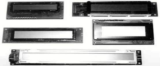 Even limited to character based modules,there is still a wide variety of shapes and sizes available. Line lenghs of 8,16,20,24,32 and 40 charecters are all standard, in one, two and four line versions.
Several different LC technologies exists. “supertwist” types, for example, offer Improved contrast and viewing angle over the older “twisted nematic” types. Some modules are available with back lighting, so so that they can be viewed in dimly-lit conditions. The back lighting may be either “electro-luminescent”, requiring a high voltage inverter circuit, or simple LED illumination.
Electrical blockdiagram:
Even limited to character based modules,there is still a wide variety of shapes and sizes available. Line lenghs of 8,16,20,24,32 and 40 charecters are all standard, in one, two and four line versions.
Several different LC technologies exists. “supertwist” types, for example, offer Improved contrast and viewing angle over the older “twisted nematic” types. Some modules are available with back lighting, so so that they can be viewed in dimly-lit conditions. The back lighting may be either “electro-luminescent”, requiring a high voltage inverter circuit, or simple LED illumination.
Electrical blockdiagram:
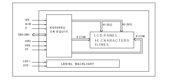 Power supply for lcd driving:
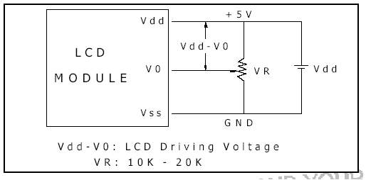 Fig 3(y):Lcd Block Diagram and Power supply circuit
3.11.2PIN DESCRIPTION:
Most LCDs with 1 controller has 14 Pins and LCDs with 2 controller has 16 Pins (two pins are extra in both for back-light LED connections).
Fig 3(y):Lcd Block Diagram and Power supply circuit
3.11.2PIN DESCRIPTION:
Most LCDs with 1 controller has 14 Pins and LCDs with 2 controller has 16 Pins (two pins are extra in both for back-light LED connections).
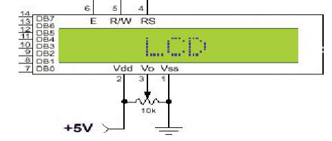 Fig3(z): pin diagram of 1x16 lines lcd
3.11.3CONTROL LINES:
EN:
Line is called "Enable." This control line is used to tell the LCD that you are sending it data. To send data to the LCD, your program should make sure this line is low (0) and then set the other two control lines and/or put data on the data bus. When the other lines are completely ready, bring EN high (1) and wait for the minimum amount of time required by the LCD datasheet (this varies from LCD to LCD), and end by bringing it low (0) again.
RS:
Line is the "Register Select" line. When RS is low (0), the data is to be treated as a command or special instruction (such as clear screen, position cursor, etc.). When RS is high (1), the data being sent is text data which sould be displayed on the screen. For example, to display the letter "T" on the screen you would set RS high.
RW:
Line is the "Read/Write" control line. When RW is low (0), the information on the data bus is being written to the LCD. When RW is high (1), the program is effectively querying (or reading) the LCD. Only one instruction ("Get LCD status") is a read command. All others are write commands, so RW will almost always be low.
Finally, the data bus consists of 4 or 8 lines (depending on the mode of operation selected by the user). In the case of an 8-bit data bus, the lines are referred to as DB0, DB1, DB2, DB3, DB4, DB5, DB6, and DB7.
Logic status on control lines:
E - 0 Access to LCD disabled. 1 Access to LCD enabled.R/W - 0 Writing data to LCD. 1 Reading data from LCD. RS - 0 Instructions
Writing data to the LCD:
1) Set R/W bit to low
2) Set RS bit to logic 0 or 1 (instruction or character)
3) Set data to data lines (if it is writing)
4) Set E line to high
5) Set E line to low
Read data from data lines (if it is reading)on LCD:
1) Set R/W bit to high
2) Set RS bit to logic 0 or 1 (instruction or character)
3) Set data to data lines (if it is writing)
4) Set E line to high
5) Set E line to low
Entering Text:
First, a little tip: it is manually a lot easier to enter characters and commands in hexadecimal rather than binary (although, of course, you will need to translate commands from binary couple of sub-miniature hexadecimal rotary switches is a simple matter, although a little bit into hex so that you know which bits you are setting). Replacing the d.i.l. switch pack with a of re-wiring is necessary.
The switches must be the type where On = 0, so that when they are turned to the zero position, all four outputs are shorted to the common pin, and in position “F”, all four outputs are open circuit.
All the available characters that are built into the module are shown in Table 3. Studying the table, you will see that codes associated with the characters are quoted in binary and hexadecimal, most significant bits (“left-hand” four bits) across the top, and least significant bits (“right-hand” four bits) down the left.
Most of the characters conform to the ASCII standard, although the Japanese and Greek characters (and a few other things) are obvious exceptions. Since these intelligent modules were designed in the “Land of the Rising Sun,” it seems only fair that their Katakana phonetic symbols should also be incorporated. The more extensive Kanji character set, which the Japanese share with the Chinese, consisting of several thousand different characters, is not included!
Using the switches, of whatever type, and referring to Table 3, enter a few characters onto the display, both letters and numbers. The RS switch (S10) must be “up” (logic 1) when sending the characters, and switch E (S9) must be pressed for each of them. Thus the operational order is: set RS high, enter character, trigger E, leave RS high, enter another character, trigger E, and so on.
The first 16 codes in Table 3, 00000000 to 00001111, ($00 to $0F) refer to the CGRAM. This is the Character Generator RAM (random access memory), which can be used to hold user-defined graphics characters. This is where these modules really start to show their potential, offering such capabilities as bar graphs, flashing symbols, even animated characters. Before the user-defined characters are set up, these codes will just bring up strange looking symbols. Codes 00010000 to 00011111 ($10 to $1F) are not used and just display blank characters. ASCII codes “proper” start at 00100000 ($20) and end with 01111111 ($7F). Codes 10000000 to 10011111 ($80 to $9F) are not used, and 10100000 to 11011111 ($A0 to $DF) are the Japanese characters.
Initialization by Instructions:
Fig3(z): pin diagram of 1x16 lines lcd
3.11.3CONTROL LINES:
EN:
Line is called "Enable." This control line is used to tell the LCD that you are sending it data. To send data to the LCD, your program should make sure this line is low (0) and then set the other two control lines and/or put data on the data bus. When the other lines are completely ready, bring EN high (1) and wait for the minimum amount of time required by the LCD datasheet (this varies from LCD to LCD), and end by bringing it low (0) again.
RS:
Line is the "Register Select" line. When RS is low (0), the data is to be treated as a command or special instruction (such as clear screen, position cursor, etc.). When RS is high (1), the data being sent is text data which sould be displayed on the screen. For example, to display the letter "T" on the screen you would set RS high.
RW:
Line is the "Read/Write" control line. When RW is low (0), the information on the data bus is being written to the LCD. When RW is high (1), the program is effectively querying (or reading) the LCD. Only one instruction ("Get LCD status") is a read command. All others are write commands, so RW will almost always be low.
Finally, the data bus consists of 4 or 8 lines (depending on the mode of operation selected by the user). In the case of an 8-bit data bus, the lines are referred to as DB0, DB1, DB2, DB3, DB4, DB5, DB6, and DB7.
Logic status on control lines:
E - 0 Access to LCD disabled. 1 Access to LCD enabled.R/W - 0 Writing data to LCD. 1 Reading data from LCD. RS - 0 Instructions
Writing data to the LCD:
1) Set R/W bit to low
2) Set RS bit to logic 0 or 1 (instruction or character)
3) Set data to data lines (if it is writing)
4) Set E line to high
5) Set E line to low
Read data from data lines (if it is reading)on LCD:
1) Set R/W bit to high
2) Set RS bit to logic 0 or 1 (instruction or character)
3) Set data to data lines (if it is writing)
4) Set E line to high
5) Set E line to low
Entering Text:
First, a little tip: it is manually a lot easier to enter characters and commands in hexadecimal rather than binary (although, of course, you will need to translate commands from binary couple of sub-miniature hexadecimal rotary switches is a simple matter, although a little bit into hex so that you know which bits you are setting). Replacing the d.i.l. switch pack with a of re-wiring is necessary.
The switches must be the type where On = 0, so that when they are turned to the zero position, all four outputs are shorted to the common pin, and in position “F”, all four outputs are open circuit.
All the available characters that are built into the module are shown in Table 3. Studying the table, you will see that codes associated with the characters are quoted in binary and hexadecimal, most significant bits (“left-hand” four bits) across the top, and least significant bits (“right-hand” four bits) down the left.
Most of the characters conform to the ASCII standard, although the Japanese and Greek characters (and a few other things) are obvious exceptions. Since these intelligent modules were designed in the “Land of the Rising Sun,” it seems only fair that their Katakana phonetic symbols should also be incorporated. The more extensive Kanji character set, which the Japanese share with the Chinese, consisting of several thousand different characters, is not included!
Using the switches, of whatever type, and referring to Table 3, enter a few characters onto the display, both letters and numbers. The RS switch (S10) must be “up” (logic 1) when sending the characters, and switch E (S9) must be pressed for each of them. Thus the operational order is: set RS high, enter character, trigger E, leave RS high, enter another character, trigger E, and so on.
The first 16 codes in Table 3, 00000000 to 00001111, ($00 to $0F) refer to the CGRAM. This is the Character Generator RAM (random access memory), which can be used to hold user-defined graphics characters. This is where these modules really start to show their potential, offering such capabilities as bar graphs, flashing symbols, even animated characters. Before the user-defined characters are set up, these codes will just bring up strange looking symbols. Codes 00010000 to 00011111 ($10 to $1F) are not used and just display blank characters. ASCII codes “proper” start at 00100000 ($20) and end with 01111111 ($7F). Codes 10000000 to 10011111 ($80 to $9F) are not used, and 10100000 to 11011111 ($A0 to $DF) are the Japanese characters.
Initialization by Instructions:
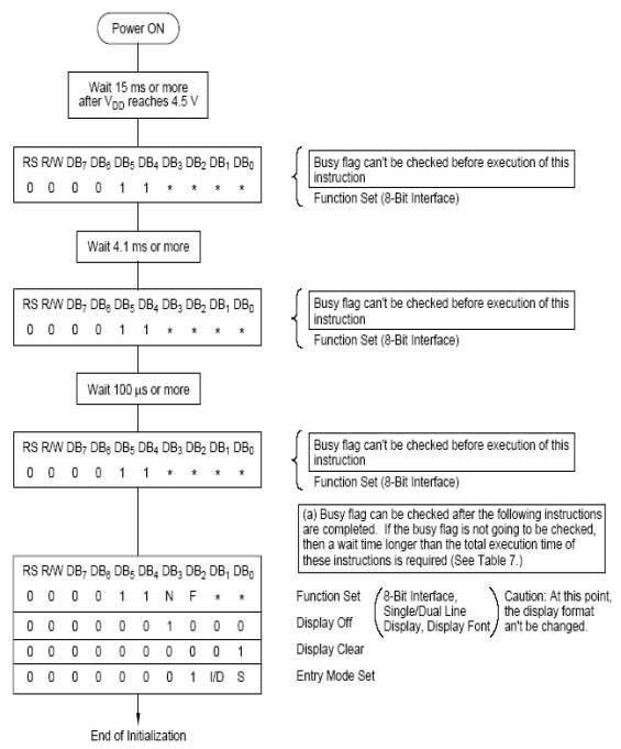 Fig 3(za):LCD Initialization Flow Diagram
If the power conditions for the normal operation of the internal reset circuit are not satisfied, then executing a series of instructions must initialize LCD unit. The procedure for this initialization process is as above show.
3.12 MAX 232
3.12.1Introduction:
A standard serial interface for PC, RS232C, requires negative logic, i.e., logic 1 is -3V to -12V and logic 0 is +3V to +12V. To convert TTL logic, say, TxD and RxD pins of the microcontroller thus need a converter chip. A MAX232 chip has long been using in many microcontrollers boards. It is a dual RS232 receiver / transmitter that meets all RS232 specifications while using only +5V power supply. It has two onboard charge pump voltage converters which generate +10V to -10V power supplies from a single 5V supply. It has four level translators, two of which are RS232 transmitters that convert TTL/CMOS input levels into +9V RS232 outputs. The other two level translators are RS232 receivers that convert RS232 input to 5V. Typical MAX232 circuit is shown below.
Fig 3(za):LCD Initialization Flow Diagram
If the power conditions for the normal operation of the internal reset circuit are not satisfied, then executing a series of instructions must initialize LCD unit. The procedure for this initialization process is as above show.
3.12 MAX 232
3.12.1Introduction:
A standard serial interface for PC, RS232C, requires negative logic, i.e., logic 1 is -3V to -12V and logic 0 is +3V to +12V. To convert TTL logic, say, TxD and RxD pins of the microcontroller thus need a converter chip. A MAX232 chip has long been using in many microcontrollers boards. It is a dual RS232 receiver / transmitter that meets all RS232 specifications while using only +5V power supply. It has two onboard charge pump voltage converters which generate +10V to -10V power supplies from a single 5V supply. It has four level translators, two of which are RS232 transmitters that convert TTL/CMOS input levels into +9V RS232 outputs. The other two level translators are RS232 receivers that convert RS232 input to 5V. Typical MAX232 circuit is shown below.
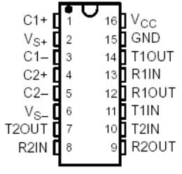
 Fig 3(zb):MAX232 IC
Cicuit connections:
A standard serial interfacing for PC, RS232C, requires negative logic, i.e., logic '1' is -3V to -12V and logic '0' is +3V to +12V. To convert a TTL logic, say, TxD and RxD pins of the uC chips, thus need a converter chip. A MAX232 chip has long been using in many uC boards. It provides 2-channel RS232C port and requires external 10uF pacitors. Carefully check the polarity of capacitor when soldering the board. A DS275 however, no need external capacitor and smaller. Either circuit can be used without any problems
3.13 LED(LIGHT EMITTING DIODE)
3.13.1 Introduction:
A light-emitting diode(LED) is a semiconductor diode that emits light when an electrical current is applied in the forward direction of the device, as in the simple LED circuit. The effect is a form of electroluminescence. where incoherent and narrow-spectrum light is emitted from the p-n junction..
LEDs are widely used as indicator lights on electronic devices and increasingly in higher power applications such as flashlights and area lighting. An LED is usually a small area (less than 1 mm2) light source, often with optics added to the chip to shape its radiation pattern and assist in reflection . The color of the emitted light depends on the composition and condition of the semi conducting material used, and can be infrared, visible, or ultraviolet. Besides lighting, interesting applications include using UV-LEDs for sterilization of water and disinfection of devices , and as a grow light to enhance photosynthesis in plants.
Basic principle:
Like a normal diode, the LED consists of a chip of semi conducting material impregnated, or doped, with impurities to create a p-n junction. As in other diodes, current flows easily from the p-side, or anode, to the n-side, or cathode, but not in the reverse direction. Charge-carriers electrons and holes flow into the junction from electrodes with different voltages. When an electron meets a hole, it falls into a lower energy level, and releases energy in the form of a photon.The wavelength of the light emitted, and therefore its color, depends on the band gap energy of the materials forming the p-n junction. In silicon or germanium diodes, the electrons and holes recombine by a non-radiative transition which produces no optical emission, because these are indirect band gap materials. The materials used for the LED have a direct band gap with energies corresponding to near-infrared, visible or near-ultraviolet light. LED development began with infrared and red devices made with gallium arsenide. Advances in materials science have made possible the production of devices with ever-shorter wavelengths, producing light in a variety of colors. LEDs are usually built on an n-type substrate, with an electrode attached to the p-type layer deposited on its surface. P-type substrates, while less common, occur as well. Many commercial LEDs, especially GaN/InGaN, also use sapphire substrate.
Fig 3(zb):MAX232 IC
Cicuit connections:
A standard serial interfacing for PC, RS232C, requires negative logic, i.e., logic '1' is -3V to -12V and logic '0' is +3V to +12V. To convert a TTL logic, say, TxD and RxD pins of the uC chips, thus need a converter chip. A MAX232 chip has long been using in many uC boards. It provides 2-channel RS232C port and requires external 10uF pacitors. Carefully check the polarity of capacitor when soldering the board. A DS275 however, no need external capacitor and smaller. Either circuit can be used without any problems
3.13 LED(LIGHT EMITTING DIODE)
3.13.1 Introduction:
A light-emitting diode(LED) is a semiconductor diode that emits light when an electrical current is applied in the forward direction of the device, as in the simple LED circuit. The effect is a form of electroluminescence. where incoherent and narrow-spectrum light is emitted from the p-n junction..
LEDs are widely used as indicator lights on electronic devices and increasingly in higher power applications such as flashlights and area lighting. An LED is usually a small area (less than 1 mm2) light source, often with optics added to the chip to shape its radiation pattern and assist in reflection . The color of the emitted light depends on the composition and condition of the semi conducting material used, and can be infrared, visible, or ultraviolet. Besides lighting, interesting applications include using UV-LEDs for sterilization of water and disinfection of devices , and as a grow light to enhance photosynthesis in plants.
Basic principle:
Like a normal diode, the LED consists of a chip of semi conducting material impregnated, or doped, with impurities to create a p-n junction. As in other diodes, current flows easily from the p-side, or anode, to the n-side, or cathode, but not in the reverse direction. Charge-carriers electrons and holes flow into the junction from electrodes with different voltages. When an electron meets a hole, it falls into a lower energy level, and releases energy in the form of a photon.The wavelength of the light emitted, and therefore its color, depends on the band gap energy of the materials forming the p-n junction. In silicon or germanium diodes, the electrons and holes recombine by a non-radiative transition which produces no optical emission, because these are indirect band gap materials. The materials used for the LED have a direct band gap with energies corresponding to near-infrared, visible or near-ultraviolet light. LED development began with infrared and red devices made with gallium arsenide. Advances in materials science have made possible the production of devices with ever-shorter wavelengths, producing light in a variety of colors. LEDs are usually built on an n-type substrate, with an electrode attached to the p-type layer deposited on its surface. P-type substrates, while less common, occur as well. Many commercial LEDs, especially GaN/InGaN, also use sapphire substrate.
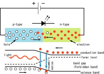 Fig 3(zc):LED
LED Display types:
Bar graph
Seven segment
Star burst
Dot matrix
Basic LED types:
Miniature LEDs
Fig 3(zc):LED
LED Display types:
Bar graph
Seven segment
Star burst
Dot matrix
Basic LED types:
Miniature LEDs
 Different sized LEDs. 8 mm, 5mm and 3 mm
These are mostly single-die LEDs used as indicators, and they come in various-size packages:
Different sized LEDs. 8 mm, 5mm and 3 mm
These are mostly single-die LEDs used as indicators, and they come in various-size packages:
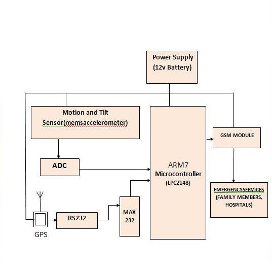 5.2Diagram:
Fig 5(a) Block Diagram of Wireless Black Box
The main principle involved in this project is the tilt and jerk detecting capability of the accelerometer. It has been in the technology world since some time and is making a large impact dueto its unique properties.
Whenever the accelerometer is tilted on any of its axis or accelerated in any direction it produces voltage outputs in accordance with it. The output of accelerometer can be provided to ADC which will sample the value and will convert it into digital data by comparing it to its predefined voltage levels. After that it will be provided to control unit built around a microcontroller. We have to set a threshold level for Accelerometer’s output to determine whether the tilt or acceleration change of vehicle is enough and exceeding the safe value to cause an accident or not.
If the control unit senses an accident situation it collects the information about that location from the GPS unit. GPS is serially interfaced with the microcontroller control unit through serial port. It serially sends data to controller about the latitude and longitude coordinates of that position. Using GSM service the control unit sends a message to the hospital’s medical services and family of the person about the accident and also send the location information collected from the GPS.
5.2Diagram:
Fig 5(a) Block Diagram of Wireless Black Box
The main principle involved in this project is the tilt and jerk detecting capability of the accelerometer. It has been in the technology world since some time and is making a large impact dueto its unique properties.
Whenever the accelerometer is tilted on any of its axis or accelerated in any direction it produces voltage outputs in accordance with it. The output of accelerometer can be provided to ADC which will sample the value and will convert it into digital data by comparing it to its predefined voltage levels. After that it will be provided to control unit built around a microcontroller. We have to set a threshold level for Accelerometer’s output to determine whether the tilt or acceleration change of vehicle is enough and exceeding the safe value to cause an accident or not.
If the control unit senses an accident situation it collects the information about that location from the GPS unit. GPS is serially interfaced with the microcontroller control unit through serial port. It serially sends data to controller about the latitude and longitude coordinates of that position. Using GSM service the control unit sends a message to the hospital’s medical services and family of the person about the accident and also send the location information collected from the GPS.
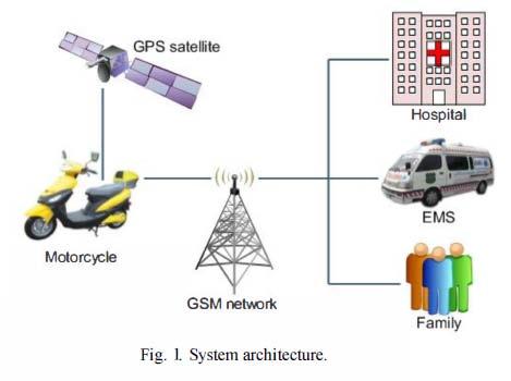 A sensor technology called the MEMS Accelerometer is used in this project to detect an accident. Accelerometer is a device which can detect a tilt or a sudden jerk in any of the 3 axis(x,y,z).It can be used to detect any unusual acceleration and tilting of vehicles which indicates that the vehicle is out of control and could have suffered an accident. The accelerometers output can be analyzed by the microcontroller to find if it has crossed the threshold.GPS system is deployed to locate the place of the accident and GSM
When any accident occur using this system accident spot can be identified by the family members and emergency services can be provided on type. If the medical services get an alert through GSM message about an accident and its location through GPS coordinates they can reach there immediately.If the person who has suffered the accident receives medical help in time he can survive the accident and many important lives can be saved. The system is easy to build and compact in size so that it can be easily installed in any vehicle.
A sensor technology called the MEMS Accelerometer is used in this project to detect an accident. Accelerometer is a device which can detect a tilt or a sudden jerk in any of the 3 axis(x,y,z).It can be used to detect any unusual acceleration and tilting of vehicles which indicates that the vehicle is out of control and could have suffered an accident. The accelerometers output can be analyzed by the microcontroller to find if it has crossed the threshold.GPS system is deployed to locate the place of the accident and GSM
When any accident occur using this system accident spot can be identified by the family members and emergency services can be provided on type. If the medical services get an alert through GSM message about an accident and its location through GPS coordinates they can reach there immediately.If the person who has suffered the accident receives medical help in time he can survive the accident and many important lives can be saved. The system is easy to build and compact in size so that it can be easily installed in any vehicle.
Fig. 3.(n):Duty Cycles of PWM
3.8.6 Power Delivery
PWM can be used to adjust the total amount of power delivered to a load without losses normally incurred when a power transfer is limited by resistive means. The drawbacks are the pulsations defined by the duty cycle, switching frequency and properties of the load. With a sufficiently high switching frequency and, when necessary, using additional passive electronic filters the pulse train can be smoothed and average analog waveform recovered.
High frequency PWM power control systems are easily realisable with semiconductor switches. As has been already stated above almost no power is dissipated by the switch in either on or off state. However, during the transitions between on and off states both voltage and current are non-zero and thus considerable power is dissipated in the switches. Luckily, the change of state between fully on and fully off is quite rapid (typically less than 100 nanoseconds) relative to typical on or
off times, and so the average power dissipation is quite low compared to the power being delivered even when high switching frequencies are used.
Modern semiconductor switches such as MOSFETs or Insulated-gate bipolar transistors (IGBTs) are quite ideal components. Thus high efficiency controllers can be built. Typically frequency converters used to control AC motors have efficiency that is better than 98 %. Switching power supplies have lower efficiency due to low output voltage levels (often even less than 2 V for microprocessors are needed) but still more than 70-80 % efficiency can be achieved. Variable-speed fan controllers for computers usually use PWM, as it is far more efficient when compared to a potentiometer or rheostat. (Neither of the latter is practical to operate electronically; they would require a small drive motor).
Light dimmers for home use employ a specific type of PWM control. Home use light dimmers typically include electronic circuitry which suppresses current flow during defined portions of each cycle of the AC line voltage. Adjusting the brightness of light emitted by a light source is then merely a matter of setting at what voltage (or phase) in the AC half cycle the dimmer begins to provide electrical current to the light source. In this case the PWM duty cycle is the ratio of the conduction time to the duration of the half AC cycle defined by the frequency of the AC line voltage.
3.8.7 Pulse Width Modulation (PWM) in ARM LPC2148
The PWM is based on the standard Timer block and inherits all of its features, although only the PWM function is pinned out on the LPC2141/2/4/6/8. The Timer is designed to count cycles of the peripheral clock (PCLK) and optionally generate interrupts or perform other actions when specified timer values occur, based on seven match registers. It also includes four capture inputs to save the timer value when an input signal transitions, and optionally generate an interrupt when those events occur. The PWM function is in addition to these features, and is based on match register events.The ability to separately control rising and falling edge locations allows the PWM to be used for more applications. For instance, multi-phase motor control typically requires three non-overlapping PWM outputs with individual control of all three pulse widths and positions.
Two match registers can be used to provide a single edge controlled PWM output. One match register (PWMMR0) controls the PWM cycle rate, by resetting the
count upon match. The other match register controls the PWM edge position. Additional single edge controlled PWM outputs require only one match register each, since the repetition rate is the same for all PWM outputs. Multiple single edge controlled PWM outputs will all have a rising edge at the beginning of each PWM cycle, when an PWMMR0 match occurs.
Three match registers can be used to provide a PWM output with both edges controlled. Again, the PWMMR0 match register controls the PWM cycle rate. The other match registers control the two PWM edge positions. Additional double edge controlled PWM outputs require only two match registers each, since the repetition rate is the same for all PWM outputs.
With double edge controlled PWM outputs, specific match registers control the rising and falling edge of the output. This allows both positive going PWM pulses (when the rising edge occurs prior to the falling edge), and negative going PWM pulses (when the falling edge occurs prior to the rising edge).
3.9 GLOBAL POSITIONING SYSTEM(GPS)
The Global Positioning System (GPS) is the only fully functional Global Navigation Satellite System (GNSS). The GPS uses a constellation of between 24 and 32 Medium Earth Orbit satellites that transmit precise microwave signals, which enable GPS receivers to determine their location, speed,. GPS was developed by the United States Department of Defense. Its official name is NAVSTAR-GPS. Although NAVSTAR-GPS is not an acronym, a few backronyms have been created for it. The GPS satellite constellation is managed by the United States Air Force 50th Space Wing.
Global Positioning System is an earth-orbiting-satellite based system that provides signals available anywhere on or above the earth, twenty-four hours a day, which can be used to determine precise time and the position of a GPS receiver in three dimensions. GPS is increasingly used as an input for Geographic Information Systems particularly for precise positioning of geospatial data and the collection of data in the field.Precise positioning is possible using GPS receivers at reference locations providing corrections and relative positioning data for remote receivers. Time and frequency dissemination, based on the precise clocks on board the SVs and controlled by the monitor stations, is another, use for GPS. Astronomical observatories telecommunications facilities and laboratory standards can be set to precise time signals or controlled to accurate frequencies by special purpose GPS receivers.
Similar satellite navigation systems include the Russian GLONASS (incomplete as of 2008), the upcoming European Galileo positioning system, the proposed COMPASS navigation system of China, and IRNSS of India.
Following the shooting down of Korean Air Lines Flight 007 in 1983, President Ronald Reagan issued a directive making the system available free for civilian use as a common good. Since then, GPS has become a widely used aid to navigation worldwide, and a useful tool for map-making, land surveying, commerce, scientific uses, and hobbies such as geocaching. GPS also provides a precise time reference used in many applications including scientific study of earthquakes, and synchronization of telecommunications networks.

 Fig 3(o) GPS satellite
3.9.1Basic concept of GPS operation
A GPS receiver calculates its position by carefully timing the signals sent by the constellation of GPS satellites high above the Earth. Each satellite continually transmits messages containing the time the message was sent, a precise orbit for the satellite sending the message (the ephemeris), and the general system health and rough orbits of all GPS satellites (the almanac). These signals travel at the speed of light through outer space, and slightly slower through the atmosphere. The receiver uses the arrival time of each message to measure the distance to each satellite, from which it determines the position of the receiver (conceptually the intersection of spheres - see trilateration ) The resulting coordinates are converted to more user-friendly forms such as latitude and longitude, or location on a map, then displayed to the user. It might seem that three satellites would be enough to solve for a position, since space has three dimensions. However, a three satellite solution requires the time be known to a nanosecond or so, far better than any non-laboratory clock can provide. Using four or more satellites allows the receiver to solve for time as well as geographical position, eliminating the need for a super accurate clock. In other words, the receiver uses four measurements to solve for four variables: x, y, z, and t. While many GPS applications have no particular use for this (very accurate) time, it is used in some GPS applications such as time transfer, and it is the only variable of interest in some applications, such as traffic signal timing. Although four satellites are required for normal operation, fewer may be needed in some special cases. If one variable is already known (for example, a ship or plane may already know its altitude), a receiver can determine its position using only three satellites. Also, in practice, receivers use additional clues (Doppler shift of satellite signals, last known position, dead reckoning, inertiral navigation, and so on) to give degraded answers when fewer than four satellites are visible.3.9.2Position calculation introduction
To provide an introductory description of how a GPS receiver works, errors will be ignored in this section. Using messages received from a minimum of four visible satellites, a GPS receiver is able to determine the satellite positions and time sent. The x, y, and z components of position and the time sent are designated aswhere the subscript i denotes the satellite number and has the value 1, 2, 3, or 4. Knowing the indicated time the message was received , the GPS receiver can compute the indicated transit time, . of the message.
Assuming the message traveled at the speed of light, c, the distance travelled, can be computed as . Knowing the distance from GPS receiver to a satellite and the position of a satellite implies that the GPS receiver is on the surface of a sphere centered at the position of a satellite. Thus we know that the indicated position of the GPS receiver is at or near the intersection of the surfaces of four spheres. In the ideal case of no errors, the GPS receiver will be at an intersection of the surfaces of four spheres. The surfaces of two spheres if they intersect in more than one point intersect in a circle. A figure, two sphere surfaces intersecting in a circle, is shown below.
 Two Sphere Surfaces Intersecting in a Circle
The article, trilateration, shows mathematically that two spheres intersecting in more than one point intersect in a circle.
Two Sphere Surfaces Intersecting in a Circle
The article, trilateration, shows mathematically that two spheres intersecting in more than one point intersect in a circle.
 Surface of Sphere Intersecting a Circle (not disk) at Two Points
A circle and sphere surface in most cases of practical interest intersects at two points, although it is conceivable that they could intersect in 0 or 1 point. Another figure, Surface of Sphere Intersecting a Circle (not disk) at Two Points, is shown to aid in visualizing this intersection. Again trilateration clearly show this mathematically. The correct position of the GPS receiver is the one that is closest to the fourth sphere.
Surface of Sphere Intersecting a Circle (not disk) at Two Points
A circle and sphere surface in most cases of practical interest intersects at two points, although it is conceivable that they could intersect in 0 or 1 point. Another figure, Surface of Sphere Intersecting a Circle (not disk) at Two Points, is shown to aid in visualizing this intersection. Again trilateration clearly show this mathematically. The correct position of the GPS receiver is the one that is closest to the fourth sphere.
3.9.3Correcting GPS clock
The method of calculating position for the case of no errors has been explained. One of the most important errors is the error in the GPS receiver clock. Because of the very large value of c, the speed of light, the estimated distances from the GPS receiver to the satellites, the pseudo ranges, are very sensitive to errors in the GPS receiver clock. This seems to suggest that an extremely accurate and expensive clock is required for the GPS receiver to work. On the other hand, manufacturers would like to make an inexpensive GPS receiver which can be mass marketed. The manufacturers were thus faced with a difficult design problem. The technique that solves this problem is based on the way sphere surfaces intersect in the GPS problem. It is likely the surfaces of the three spheres intersect since the circle of intersection of the first two spheres is normally quite large and thus the third sphere surface is likely to intersect this large circle. It is very unlikely that the surface of the sphere corresponding to the fourth satellite will intersect either of the two points of intersection of the first three since any clock error could cause it to miss intersecting a point. However the distance from the valid estimate of GPS receiver position to the surface of the sphere corresponding to the fourth satellite can be used to compute a clock correction. Letdenote the distance from the valid estimate of GPS receiver position to the fourth satellite and let denote the pseudo range of the fourth satellite. Let . Note that is the distance from the computed GPS receiver position to the surface of the sphere corresponding to the fourth satellite. Thus the quotient, , provides an estimate of:
(correct time) - (time indicated by the receiver's on-board clock)
and the GPS receiver clock can be advanced if is positive or delayed if is negative.
3.9.4System segmentation
The current GPS consists of three major segments. These are the space segment (SS), a control segment (CS), and a user segment (US). 3.9.5Space segment Fig 3(p) GPS Constellation
A visual example of the GPS constellation in motion with the Earth rotating. Notice how the number of satellites in view from a given point on the Earth's surface, in this example at 45°N, changes with time.
The space segment (SS) comprises the orbiting GPS satellites, or Space Vehicles (SV) in GPS parlance. The GPS design originally called for 24 SVs, eight each in three circular orbital planes, but this was modified to six planes with four satellites each. The orbital
Figure 3(q): A GPS satellite
planes are centered on the Earth, not rotating with respect to the distant stars. The six planes have approximately 55° inclination (tilt relative to Earth's equator) and are separated by 60° right ascension of the ascending node (angle along the equator from a reference point to the orbit's intersection). The orbits are arranged so that at least six satellites are always within line of sight from almost everywhere on Earth's surface.
Orbiting at an altitude of approximately 20,200 kilometers (12,600 miles or 10,900 nautical miles; orbital radius of 26,600 km (16,500 mi or 14,400 NM)), each SV makes two complete orbits each sidereal day. The ground track of each satellite therefore repeats each (sidereal) day. This was very helpful during development, since even with just four satellites, correct alignment means all four are visible from one spot for a few hours each day. For military operations, the ground track repeat can be used to ensure good coverage in combat zones.
As of March 2008, there are 31 actively broadcasting satellites in the GPS constellation. The additional satellites improve the precision of GPS receiver calculations by providing redundant measurements. With the increased number of satellites, the constellation was changed to a nonuniform arrangement. Such an arrangement was shown to improve reliability and availability of the system, relative to a uniform system, when multiple satellites fail.
Some reports in 2008 indicated that the 32nd satellite was causing difficulties for some GPS receivers.
Fig 3(p) GPS Constellation
A visual example of the GPS constellation in motion with the Earth rotating. Notice how the number of satellites in view from a given point on the Earth's surface, in this example at 45°N, changes with time.
The space segment (SS) comprises the orbiting GPS satellites, or Space Vehicles (SV) in GPS parlance. The GPS design originally called for 24 SVs, eight each in three circular orbital planes, but this was modified to six planes with four satellites each. The orbital
Figure 3(q): A GPS satellite
planes are centered on the Earth, not rotating with respect to the distant stars. The six planes have approximately 55° inclination (tilt relative to Earth's equator) and are separated by 60° right ascension of the ascending node (angle along the equator from a reference point to the orbit's intersection). The orbits are arranged so that at least six satellites are always within line of sight from almost everywhere on Earth's surface.
Orbiting at an altitude of approximately 20,200 kilometers (12,600 miles or 10,900 nautical miles; orbital radius of 26,600 km (16,500 mi or 14,400 NM)), each SV makes two complete orbits each sidereal day. The ground track of each satellite therefore repeats each (sidereal) day. This was very helpful during development, since even with just four satellites, correct alignment means all four are visible from one spot for a few hours each day. For military operations, the ground track repeat can be used to ensure good coverage in combat zones.
As of March 2008, there are 31 actively broadcasting satellites in the GPS constellation. The additional satellites improve the precision of GPS receiver calculations by providing redundant measurements. With the increased number of satellites, the constellation was changed to a nonuniform arrangement. Such an arrangement was shown to improve reliability and availability of the system, relative to a uniform system, when multiple satellites fail.
Some reports in 2008 indicated that the 32nd satellite was causing difficulties for some GPS receivers.
3.9.6Control segment
The flight paths of the satellites are tracked by US Air Force monitoring stations in Hawaii, Kwajalein, Ascension Island, Diego Garcia, and Colorado Springs, Colorado, along with monitor stations operated by the National Geospatial-Intelligence Agency (NGA). The tracking information is sent to the Air Force Space Command's master control station at Schriever Air Force Base in Colorado Springs, which is operated by the 2nd Space Operations Squadron (2 SOPS) of the United States Air Force (USAF). Then 2 SOPS contacts each GPS satellite regularly with a navigational update (using the ground antennas at Ascension Island, Diego Garcia, Kwajalein, and Colorado Springs). These updates synchronize the atomic clocks on board the satellites to within a few nanoseconds of each other, and adjust the ephemeris of each satellite's internal orbital model. The updates are created by a Kalman filter which uses inputs from the ground monitoring stations, space weather information, and various other inputs. Satellite maneuvers are not precise by GPS standards. So to change the orbit of a satellite, the satellite must be marked 'unhealthy', so receivers will not use it in their calculation. Then the maneuver can be carried out, and the resulting orbit tracked from the ground. Then the new ephemeris is uploaded and the satellite marked healthy again. User segment PS receivers come in a variety of formats, from devices integrated into cars, phones, and watches, to dedicated devices such as those shown here from manufacturers Trimble, Garmin and Leica (left to right). The user's GPS receiver is the user segment (US) of the GPS. In general, GPS receivers are composed of an antenna, tuned to the frequencies transmitted by the satellites, receiver-processors, and a highly-stable clock (often a crystal oscillator). They may also include a display for providing location and speed information to the user. A receiver is often described by its number of channels: this signifies how many satellites it can monitor simultaneously. Originally limited to four or five, this has progressively increased over the years so that, as of 2007, receivers typically have between 12 and 20 channels. A typical OEM GPS receiver module measuring 15×17 mm.
GPS receivers may include an input for differential corrections, using the RTCM SC-104 format. This is typically in the form of a RS-232 port at 4,800 bit/s speed. Data is actually sent at a much lower rate, which limits the accuracy of the signal sent using RTCM. Receivers with internal DGPS receivers can outperform those using external RTCM data. As of 2006, even low-cost units commonly include Wide Area Augmentation System (WAAS) receivers.
A typical OEM GPS receiver module measuring 15×17 mm.
GPS receivers may include an input for differential corrections, using the RTCM SC-104 format. This is typically in the form of a RS-232 port at 4,800 bit/s speed. Data is actually sent at a much lower rate, which limits the accuracy of the signal sent using RTCM. Receivers with internal DGPS receivers can outperform those using external RTCM data. As of 2006, even low-cost units commonly include Wide Area Augmentation System (WAAS) receivers.
 Fig 3(r)A typical GPS receiver with integrated antenna.
Many GPS receivers can relay position data to a PC or other device using the NMEA 0183 protocol, or the newer and less widely used NMEA 2000. Although these protocols are officially defined by the NMEA, references to the these protocols have been compiled from public records, allowing open source tools like gpsd to read the protocol without violating intellectual property laws. Other proprietary protocols exist as well, such as the SiRF and MTK protocols. Receivers can interface with other devices using methods including a serial connection, USB or Bluetooth.
Fig 3(r)A typical GPS receiver with integrated antenna.
Many GPS receivers can relay position data to a PC or other device using the NMEA 0183 protocol, or the newer and less widely used NMEA 2000. Although these protocols are officially defined by the NMEA, references to the these protocols have been compiled from public records, allowing open source tools like gpsd to read the protocol without violating intellectual property laws. Other proprietary protocols exist as well, such as the SiRF and MTK protocols. Receivers can interface with other devices using methods including a serial connection, USB or Bluetooth.
Navigation signals
 Fig 3(s)GPS broadcast signal
Each GPS satellite continuously broadcasts a Navigation Message at 50 bit/s giving the time-of-week, GPS week number and satellite health information (all transmitted in the first part of the message), an ephemeris (transmitted in the second part of the message) and an almanac (later part of the message). The messages are sent in frames, each taking 30 seconds to transmit 1500 bits.
The first 6 seconds of every frame contains data describing the satellite clock and its relationship to GPS time. The next 12 seconds contain the ephemeris data, giving the satellite's own precise orbit. The ephemeris is updated every 2 hours and is generally valid for 4 hours, with provisions for updates every 6 hours or longer in non-nominal conditions. The time needed to acquire the ephemeris is becoming a significant element of the delay to first position fix, because, as the hardware becomes more capable, the time to lock onto the satellite signals shrinks, but the ephemeris data requires 30 seconds (worst case) before it is received, due to the low data transmission rate.
The almanac consists of coarse orbit and status information for each satellite in the constellation, an ionosphere model, and information to relate GPS derived time to Coordinated Universal Time (UTC). A new part of the almanac is received for the last 12 seconds in each 30 second frame. Each frame contains 1/25th of the almanac, so 12.5 minutes are required to receive the entire almanac from a single satellite. The almanac serves several purposes. The first is to assist in the acquisition of satellites at power-up by allowing the receiver to generate a list of visible satellites based on stored position and time, while an ephemeris from each satellite is needed to compute position fixes using that satellite. In older hardware, lack of an almanac in a new receiver would cause long delays before providing a valid position, because the search for each satellite was a slow process. Advances in hardware have made the acquisition process much faster, so not having an almanac is no longer an issue. The second purpose is for relating time derived from the GPS (called GPS time) to the international time standard of UTC. Finally, the almanac allows a single frequency receiver to correct for ionospheric error by using a global ionospheric model. The corrections are not as accurate as augmentation systems like WAAS or dual frequency receivers. However it is often better than no correction since ionospheric error is the largest error source for a single frequency GPS receiver. An important thing to note about navigation data is that each satellite transmits only its own ephemeris, but transmits an almanac for all satellites.
Each satellite transmits its navigation message with at least two distinct spread spectrum codes: the Coarse / Acquisition (C/A) code, which is freely available to the public, and the Precise (P) code, which is usually encrypted and reserved for military applications. The C/A code is a 1023 length Gold code at 1.023 million chips per second so that it repeats every millisecond. As pointed out in a chip is essentially the same thing as a bit and chips per second are the same as bits per second. The justification for coming up with this new term, chip, is that in some cases a sequence of bits is used as a type of Modulation and contains no information.
Each satellite has its own C/A code so that it can be uniquely identified and received separately from the other satellites transmitting on the same frequency. The P-code is a 10.23 mega chip per second PRN code that repeats only every week. When the "anti-spoofing" mode is on, as it is in normal operation, the P code is encrypted by the Y-code to produce the P(Y) code, which can only be decrypted by units with a valid decryption key. Both the C/A and P(Y) codes impart the precise time-of-day to the user.
Fig 3(s)GPS broadcast signal
Each GPS satellite continuously broadcasts a Navigation Message at 50 bit/s giving the time-of-week, GPS week number and satellite health information (all transmitted in the first part of the message), an ephemeris (transmitted in the second part of the message) and an almanac (later part of the message). The messages are sent in frames, each taking 30 seconds to transmit 1500 bits.
The first 6 seconds of every frame contains data describing the satellite clock and its relationship to GPS time. The next 12 seconds contain the ephemeris data, giving the satellite's own precise orbit. The ephemeris is updated every 2 hours and is generally valid for 4 hours, with provisions for updates every 6 hours or longer in non-nominal conditions. The time needed to acquire the ephemeris is becoming a significant element of the delay to first position fix, because, as the hardware becomes more capable, the time to lock onto the satellite signals shrinks, but the ephemeris data requires 30 seconds (worst case) before it is received, due to the low data transmission rate.
The almanac consists of coarse orbit and status information for each satellite in the constellation, an ionosphere model, and information to relate GPS derived time to Coordinated Universal Time (UTC). A new part of the almanac is received for the last 12 seconds in each 30 second frame. Each frame contains 1/25th of the almanac, so 12.5 minutes are required to receive the entire almanac from a single satellite. The almanac serves several purposes. The first is to assist in the acquisition of satellites at power-up by allowing the receiver to generate a list of visible satellites based on stored position and time, while an ephemeris from each satellite is needed to compute position fixes using that satellite. In older hardware, lack of an almanac in a new receiver would cause long delays before providing a valid position, because the search for each satellite was a slow process. Advances in hardware have made the acquisition process much faster, so not having an almanac is no longer an issue. The second purpose is for relating time derived from the GPS (called GPS time) to the international time standard of UTC. Finally, the almanac allows a single frequency receiver to correct for ionospheric error by using a global ionospheric model. The corrections are not as accurate as augmentation systems like WAAS or dual frequency receivers. However it is often better than no correction since ionospheric error is the largest error source for a single frequency GPS receiver. An important thing to note about navigation data is that each satellite transmits only its own ephemeris, but transmits an almanac for all satellites.
Each satellite transmits its navigation message with at least two distinct spread spectrum codes: the Coarse / Acquisition (C/A) code, which is freely available to the public, and the Precise (P) code, which is usually encrypted and reserved for military applications. The C/A code is a 1023 length Gold code at 1.023 million chips per second so that it repeats every millisecond. As pointed out in a chip is essentially the same thing as a bit and chips per second are the same as bits per second. The justification for coming up with this new term, chip, is that in some cases a sequence of bits is used as a type of Modulation and contains no information.
Each satellite has its own C/A code so that it can be uniquely identified and received separately from the other satellites transmitting on the same frequency. The P-code is a 10.23 mega chip per second PRN code that repeats only every week. When the "anti-spoofing" mode is on, as it is in normal operation, the P code is encrypted by the Y-code to produce the P(Y) code, which can only be decrypted by units with a valid decryption key. Both the C/A and P(Y) codes impart the precise time-of-day to the user.
3.9.7 Position determination
Before providing a more mathematical description of position calculation, the introductory material on these topics is reviewed. To describe the basic concept of how a GPS receiver works, the errors are at first ignored. Using messages received from four satellites, the GPS receiver is able to determine the satellite positions and time sent. The x, y, and z components of position and the time sent are designated aswhere the subscript i denotes which satellite and has the value 1, 2, 3, or 4. Knowing the indicated time the message was received, the GPS receiver can compute the indicated transit time, . of the message. Assuming the message traveled at the speed of light, c, the distance traveled, can be computed as . Knowing the distance from GPS receiver to a satellite and the position of a satellite implies that the GPS receiver is on the surface of a sphere centered at the position of a satellite. Thus we know that the indicated position of the GPS receiver is at or near the intersection of the surfaces of four spheres. In the ideal case of no errors, the GPS receiver will be at an intersection of the surfaces of four spheres. The surfaces of two spheres if they intersect in more than one point intersect in a circle. A figure, Two Sphere Surfaces Intersecting in a Circle, is shown below depicting this which hopefully will aid the reader in visualizing this intersection.
Two Sphere Surfaces Intersecting in a Circle
Three dimensional co-ordinate system
Fig 3(t) 3 Dimensional GPS System
The article, trilateration, shows mathematically how the equation for a circle is determined. A circle and sphere surface in most cases of practical interest intersects at two points, although it is conceivable that they could intersect in 0 or 1 point. Another figure, Surface of Sphere Intersecting a Circle (not disk) at Two Points, is shown below to aid in visualizing this intersection. Again trilateration clearly show this mathematically. The correct position of the GPS receiver is the one that is closest to the fourth sphere. This paragraph has described the basic concept of GPS while ignoring errors. The next problem is how to process the messages when errors are present.
Surface of Sphere Intersecting a Circle (not disk) at Two Points
Let denote the clock error or bias, the amount by which the receiver's clock is slow. The GPS receiver has four unknowns, the three components of GPS receiver position and the clock bias . The equation of the sphere surfaces are given by:
Another useful form of these equations is in terms of the pseudoranges, which are simply the ranges approximated based on GPS receiver clock's indicated (i.e. uncorrected) time so that . Then the equations becomes:
.
Two of the most important methods of computing GPS receiver position and clock bias are (1) trilateration followed by one dimensional numerical root finding and (2) multidimensional Newton-Raphson. These two methods along with their advantages are discussed.
solve by trilateration followed by one dimensional numerical root finding. This method involves using Trilateration to determine the intersection of the surfaces of three spheres. It is clearly shown in trilateration that the surfaces of three spheres intersect in 0, 1, or 2 points. In the usual case of two intersections, the solution which is nearest the surface of the sphere corresponding to the fourth satellite is chosen. The surface of the earth can also sometimes be used instead, especially in the case of civilian GPS receivers since it is illegal in the United States to track vehicles of more than 60,000 feet in altitude. The bias,is then computed based on the distance from the solution to the surface of the sphere corresponding to the fourth satellite. Using an updated received time based on this bias, new spheres are computed and the process is repeated. One advantage of this method is that it involves one dimensional as opposed to multidimensional numerical root finding.
Utilize multidimensional Newton-Raphson. Linearize around an approximate solution say from iteration k, then solve four linear equations derived from the quadratic equations above to obtain . The radii are large and so the sphere surfaces are close to flat. This near flatness may cause the iterative procedure to converge rapidly in the case where is near the correct value and the primary change is in the values of , since in this case the problem is merely to find the intersection of nearly flat surfaces and thus close to a linear problem. However when is changing significantly, this near flatness does not appear to be advantageous in producing rapid convergence, since in this case these near flat surfaces will be moving as the spheres expand and contract. This possible fast convergence is an advantage of this method. Also it has been claimed that this method is the "typical" method used by GPS receivers. A disadvantage of this method is that according to, "There are no good general methods for solving systems of more than one nonlinear equation."
Other methods include: Solve for the intersection of the expanding signals form light cones in 4-space cones, Solve for the intersection of hyperboloids determined by the time difference of signals received from satellites utilizing multilateration, Solve the equations in accordance with.
More than four satellites should be used, if available. This results in an over-determined system of equations with no unique solution, which must be solved by least-squares or a similar technique. If all visible satellites are used, the results are always at least as good as using the four best, and usually better. Also the errors in results can be estimated through the residuals. With each combination of four or more satellites, a geometric dilution of precision (GDOP) vector can be calculated, based on the relative sky positions of the satellites used. As more satellites are picked up, pseudoranges from more combinations of four satellites can be processed to add more estimates to the location and clock offset. The receiver then determines which combinations to use and how to calculate the estimated position by determining the weighted average of these positions and clock offsets. After the final location and time are calculated, the location is expressed in a specific coordinate system such as latitude and longitude, using the WGS 84 geodetic datum or a local system specific to a country.
Finally, results from other positioning systems such as GLONASS or the upcoming Galileo can be used in the fit, or used to double check the result. (By design, these systems use the same bands; so much of the receiver circuitry can be shared, though the decoding is different.
3.10 GSM (Global System for Mobile communications)
GSM (Global System for Mobile communications) is a cellular network, which means that mobile phones connect to it by searching for cells in the immediate vicinity. GSM networks operate in four different frequency ranges. Most GSM networks operate in the 900 MHz or 1800 MHz bands. Some countries in the Americas use the 850 MHz and 1900 MHz bands because the 900 and 1800 MHz frequency bands were already allocated.
The rarer 400 and 450 MHz frequency bands are assigned in some countries, where these frequencies were previously used for first-generation systems.
GSM-900 uses 890–915 MHz to send information from the mobile station to the base station (uplink) and 935–960 MHz for the other direction (downlink), providing 124 RF channels (channel numbers 1 to 124) spaced at 200 kHz. Duplex spacing of 45 MHz is used. In some countries the GSM-900 band has been extended to cover a larger frequency range. This 'extended GSM', E-GSM, uses 880–915 MHz (uplink) and 925–960 MHz (downlink), adding 50 channels (channel numbers 975 to 1023 and 0) to the original GSM-900 band. Time division multiplexing is used to allow eight full-rate or sixteen half-rate speech channels per radio frequency channel. There are eight radio timeslots (giving eight burst periods) grouped into what is called a TDMA frame. Half rate channels use alternate frames in the same timeslot. The channel data rate is 270.833 kbit/s, and the frame duration is 4.615 ms.
3.10.1GSM Advantages:
GSM also pioneered a low-cost, to the network carrier, alternative to voice calls, the Short t message service (SMS, also called "text messaging"), which is now supported on other mobile standards as well. Another advantage is that the standard includes one worldwide Emergency telephone number, 112. This makes it easier for international travelers to connect to emergency services without knowing the local emergency number.
3.10.2The GSM Network:
GSM provides recommendations, not requirements. The GSM specifications define the functions and interface requirements in detail but do not address the hardware. The GSM network is divided into three major systems: the switching system (SS), the base station system (BSS), and the operation and support system (OSS).
Fig 3(u) GSM Network
3.10.3 The Switching System:
The switching system (SS) is responsible for performing call processing and subscriber-related functions. The switching system includes the following functional units. Home location register (HLR): The HLR is a database used for storage and management of subscriptions. The HLR is considered the most important database, as it stores permanent data about subscribers, including a subscriber's service profile, location information, and activity status. When an individual buys a subscription from one of the PCS operators, he or she is registered in the HLR of that operator. Mobile services switching center (MSC): The MSC performs the telephony switching functions of the system. It controls calls to and from other telephone and data systems. It also performs such functions as toll ticketing, network interfacing, common channel signaling, and others. Visitor location register (VLR): The VLR is a database that contains temporary information about subscribers that is needed by the MSC in order to service visiting subscribers. The VLR is always integrated with the MSC. When a mobile station roams into a new MSC area, the VLR connected to that MSC will request data about the mobile station from the HLR. Later, if the mobile station makes a call, the VLR will have the information needed for call setup without having to interrogate the HLR each time. Authentication center (AUC): A unit called the AUC provides authentication and encryption parameters that verify the user's identity and ensure the confidentiality of each call. The AUC protects network operators from different types of fraud found in today's cellular world. Equipment identity register (EIR): The EIR is a database that contains information about the identity of mobile equipment that prevents calls from stolen, unauthorized, or defective mobile stations. The AUC and EIR are implemented as stand-alone nodes or as a combined AUC/EIR node.3.10.4 The Base Station System (BSS):
All radio-related functions are performed in the BSS, which consists of base station controllers (BSCs) and the base transceiver stations (BTSs). BSC: The BSC provides all the control functions and physical links between the MSC and BTS. It is a high-capacity switch that provides functions such as handover, cell configuration data, and control of radio frequency (RF) power levels in base transceiver stations. A number of BSCs are served by an MSC. BTS: The BTS handles the radio interface to the mobile station. The BTS is the radio equipment (transceivers and antennas) needed to service each cell in the network. A group of BTSs are controlled by a BSC.3.10.5The Operation and Support System
The operations and maintenance center (OMC) is connected to all equipment in the switching system and to the BSC. The implementation of OMC is called the operation and support system (OSS). The OSS is the functional entity from which the network operator monitors and controls the system. The purpose of OSS is to offer the customer cost-effective support for centralized, regional and local operational and maintenance activities that are required for a GSM network. An important function of OSS is to provide a network overview and support the maintenance activities of different operation and maintenance organizations.3.10.6 Additional Functional Elements
Message center (MXE): The MXE is a node that provides integrated voice, fax, and data messaging. Specifically, the MXE handles short message service, cell broadcast, voice mail, fax mail, e-mail, and notification. Mobile service node (MSN): The MSN is the node that handles the mobile intelligent network (IN) services. Gateway mobile services switching center (GMSC): A gateway is a node used to interconnect two networks. The gateway is often implemented in an MSC. The MSC is then referred to as the GMSC. GSM inter-working unit (GIWU): The GIWU consists of both hardware and software that provides an interface to various networks for data communications. Through the GIWU, users can alternate between speech and data during the same call. The GIWU hardware equipment is physically located at the MSC/VLR. 3.10.7GSM Network Areas: The GSM network is made up of geographic areas. As shown in bellow figure, these areas include cells, location areas (LAs), MSC/VLR service areas, and public land mobile network (PLMN) areas.
Fig 3(v): GSM Network Area
Location Areas:
The cell is the area given radio coverage by one base transceiver station. The GSM network identifies each cell via the cell global identity (CGI) number assigned to each cell. The location area is a group of cells. It is the area in which the subscriber is paged. Each LA is served by one or more base station controllers, yet only by a single MSC Each LA is assigned a location area identity (LAI) number.
MSC/VLR service areas:
An MSC/VLR service area represents the part of the GSM network that is covered by one MSC and which is reachable, as it is registered in the VLR of the MSC.
PLMN service areas:
The PLMN service area is an area served by one network operator.
3.10.8GSM Specifications:
Specifications for different personal communication services (PCS) systems vary among the different PCS networks. Listed below is a description of the specifications and characteristics for GSM.
Frequency band: The frequency range specified for GSM is 1,850 to 1,990 MHz (mobile station to base station).
Duplex distance: The duplex distance is 80 MHz. Duplex distance is the distance between the uplink and downlink frequencies. A channel has two frequencies, 80 MHz apart.
Channel separation: The separation between adjacent carrier frequencies. In GSM, this is 200 kHz.
Modulation: Modulation is the process of sending a signal by changing the characteristics of a carrier frequency. This is done in GSM via Gaussian minimum shift keying (GMSK).
Transmission rate: GSM is a digital system with an over-the-air bit rate of 270 kbps.
Access method: GSM utilizes the time division multiple access (TDMA) concept. TDMA is a technique in which several different calls may share the same carrier. Each call is assigned a particular time slot.
Speech coder: GSM uses linear predictive coding (LPC). The purpose of LPC is to reduce the bit rate. The LPC provides parameters for a filter that mimics the vocal tract. The signal passes through this filter, leaving behind a residual signal. Speech is encoded at 13 kbps.
3.10.9 GSM Subscriber Services:
Dual-tone multifrequency (DTMF): DTMF is a tone signaling scheme often used for various control purposes via the telephone network, such as remote control of an answering machine. GSM supports full-originating DTMF.
Facsimile group III—GSM supports CCITT Group 3 facsimile. As standard fax machines are designed to be connected to a telephone using analog signals, a special fax converter connected to the exchange is used in the GSM system. This enables a GSM–connected fax to communicate with any analog fax in the network.
Short message services: A convenient facility of the GSM network is the short message service. A message consisting of a maximum of 160 alphanumeric characters can be sent to or from a mobile station. This service can be viewed as an advanced form of alphanumeric paging with a number of advantages. If the subscriber's mobile unit is powered off or has left the coverage area, the message is stored and offered back to the subscriber when the mobile is powered on or has reentered the coverage area of the network. This function ensures that the message will be received.
Cell broadcast: A variation of the short message service is the cell broadcast facility. A message of a maximum of 93 characters can be broadcast to all mobile subscribers in a certain geographic area. Typical applications include traffic congestion warnings and reports on accidents.
Voice mail: This service is actually an answering machine within the network, which is controlled by the subscriber. Calls can be forwarded to the subscriber's voice-mail box and the subscriber checks for messages via a personal security code.
Fax mail: With this service, the subscriber can receive fax messages at any fax machine. The messages are stored in a service center from which they can be retrieved by the subscriber via a personal security code to the desired fax number
Supplementary Services:
GSM supports a comprehensive set of supplementary services that can complement and support both telephony and data services. Call forwarding: This service gives the subscriber the ability to forward incoming calls to another number if the called mobile unit is not reachable, if it is busy, if there is no reply, or if call forwarding is allowed unconditionally. Barring of outgoing calls: This service makes it possible for a mobile subscriber to prevent all outgoing calls. Barring of incoming calls: This function allows the subscriber to prevent incoming calls. The following two conditions for incoming call barring exist: baring of all incoming calls and barring of incoming calls when roaming outside the home PLMN. Advice of charge (AoC): The AoC service provides the mobile subscriber with an estimate of the call charges. There are two types of AoC information: one that provides the subscriber with an estimate of the bill and one that can be used for immediate charging purposes. AoC for data calls is provided on the basis of time measurements. Call hold: This service enables the subscriber to interrupt an ongoing call and then subsequently reestablish the call. The call hold service is only applicable to normal telephony. Call waiting: This service enables the mobile subscriber to be notified of an incoming call during a conversation. The subscriber can answer, reject, or ignore the incoming call. Call waiting is applicable to all GSM telecommunications services using a circuit-switched connection. Multiparty service: The multiparty service enables a mobile subscriber to establish a multiparty conversation—that is, a simultaneous conversation between three and six subscribers. This service is only applicable to normal telephony. Calling line identification presentation/restriction: These services supply the called party with the integrated services digital network (ISDN) number of the calling party. The restriction service enables the calling party to restrict the presentation. The restriction overrides the presentation. Closed user groups (CUGs): CUGs are generally comparable to a PBX. They are a group of subscribers who are capable of only calling themselves and certain numbers 3.10.10Main AT commands: "AT command set for GSM Mobile Equipment” describes the Main AT commands to communicate via a serial interface with the GSM subsystem of the phone. AT commands are instructions used to control a modem. AT is the abbreviation of Attention. Every command line starts with "AT" or "at". That's why modem commands are called AT commands. Many of the commands that are used to control wired dial-up modems, such as ATD (Dial), ATA (Answer), ATH (Hook control) and ATO (Return to online data state), are also supported by GSM/GPRS modems and mobile phones. Besides this common AT command set, GSM/GPRS modems and mobile phones support an AT command set that is specific to the GSM technology, which includes SMS-related commands like AT+CMGS (Send SMS message), AT+CMSS (Send SMS message from storage), AT+CMGL (List SMS messages) and AT+CMGR (Read SMS messages). Note that the starting "AT" is the prefix that informs the modem about the start of a command line. It is not part of the AT command name. For example, D is the actual AT command name in ATD and +CMGS is the actual AT command name in AT+CMGS. However, some books and web sites use them interchangeably as the name of an AT command. Here are some of the tasks that can be done using AT commands with a GSM/GPRS modem or mobile phone:Get basic information about the mobile phone or GSM/GPRS modem. For example, name of manufacturer (AT+CGMI), model number (AT+CGMM), IMEI number (International Mobile Equipment Identity) (AT+CGSN) and software version (AT+CGMR). Get basic information about the subscriber. For example, MSISDN (AT+CNUM) and IMSI number (International Mobile Subscriber Identity) (AT+CIMI).Get the current status of the mobile phone or GSM/GPRS modem. For example, mobile phone activity status (AT+CPAS), mobile network registration status (AT+CREG), radio signal strength (AT+CSQ), battery charge level and battery charging status (AT+CBC). Establish a data connection or voice connection to a remote modem (ATD, ATA, etc).Send and receive fax (ATD, ATA, AT+F*).Send (AT+CMGS, AT+CMSS), read (AT+CMGR, AT+CMGL), write (AT+CMGW) or delete (AT+CMGD) SMS messages and obtain notifications of newly received SMS messages (AT+CNMI).Read (AT+CPBR), write (AT+CPBW) or search (AT+CPBF) phonebook entries.Perform security-related tasks, such as opening or closing facility locks (AT+CLCK), checking whether a facility is locked (AT+CLCK) and changing passwords (AT+CPWD). (Facility lock examples: SIM lock [a password must be given to the SIM card every time the mobile phone is switched on] and PH-SIM lock [a certain SIM card is associated with the mobile phone. To use other SIM cards with the mobile phone, a password must be entered.]) Control the presentation of result codes / error messages of AT commands. For example, you can control whether to enable certain error messages (AT+CMEE) and whether error messages should be displayed in numeric format or verbose format (AT+CMEE=1 or AT+CMEE=2).Get or change the configurations of the mobile phone or GSM/GPRS modem. For example, change the GSM network (AT+COPS), bearer service type (AT+CBST), radio link protocol parameters (AT+CRLP), SMS center address (AT+CSCA) and storage of SMS messages (AT+CPMS).Save and restore configurations of the mobile phone or GSM/GPRS modem. For example, save (AT+CSAS) and restore (AT+CRES) settings related to SMS messaging such as the SMS center address. 3.11 LCD (Liquid Cristal Display) 3.11.1 INTRODUCTION: A liquid crystal display (LCD) is a thin, flat display device made up of any number of color or monochrome pixels arrayed in front of a light source or reflector. Each pixel consists of a column of liquid crystal molecules suspended between two transparent electrodes, and two polarizing filters, the axes of polarity of which are perpendicular to each other. Without the liquid crystals between them, light passing through one would be blocked by the other. The liquid crystal twists the polarization of light entering one filter to allow it to pass through the other. A program must interact with the outside world using input and output devices that communicate directly with a human being. One of the most common devices attached to an controller is an LCD display. Some of the most common LCDs connected to the contollers are 16X1, 16x2 and 20x2 displays. This means 16 characters per line by 1 line 16 characters per line by 2 lines and 20 characters per line by 2 lines, respectively.
Shapes and S
available. Line lengths of 8, 16, 20, 24, 32 and 40 characters are all standard, in one, two
Many microcontroller devices use 'smart LCD' displays to output visual information. LCD displays designed around LCD NT-C1611 module, are inexpensive, easy to use, and it is even possible to produce a readout using the 5X7 dots plus cursor of the display. They have a standard ASCII set of characters and mathematical symbols. For an 8-bit data bus, the display requires a +5V supply plus 10 I/O lines (RS RW D7 D6 D5 D4 D3 D2 D1 D0). For a 4-bit data bus it only requires the supply lines plus 6 extra lines(RS RW D7 D6 D5 D4). When the LCD display is not enabled, data lines are tri-state and they do not interfere with the operation of the microcontroller.
Features:
Interface with either 4-bit or 8-bit microprocessor. Display data RAM (80 characters). Character generator ROM. 160 different 5 7 dot-matrix character patterns.Character generator RAM
Fig 3(x): Address locations for a 1x16 line LCD
Shapes and sizes:
Even limited to character based modules,there is still a wide variety of shapes and sizes available. Line lenghs of 8,16,20,24,32 and 40 charecters are all standard, in one, two and four line versions.
Several different LC technologies exists. “supertwist” types, for example, offer Improved contrast and viewing angle over the older “twisted nematic” types. Some modules are available with back lighting, so so that they can be viewed in dimly-lit conditions. The back lighting may be either “electro-luminescent”, requiring a high voltage inverter circuit, or simple LED illumination.
Electrical blockdiagram:
Power supply for lcd driving:
Fig 3(y):Lcd Block Diagram and Power supply circuit
3.11.2PIN DESCRIPTION:
Most LCDs with 1 controller has 14 Pins and LCDs with 2 controller has 16 Pins (two pins are extra in both for back-light LED connections).
Fig3(z): pin diagram of 1x16 lines lcd
3.11.3CONTROL LINES:
EN:
Line is called "Enable." This control line is used to tell the LCD that you are sending it data. To send data to the LCD, your program should make sure this line is low (0) and then set the other two control lines and/or put data on the data bus. When the other lines are completely ready, bring EN high (1) and wait for the minimum amount of time required by the LCD datasheet (this varies from LCD to LCD), and end by bringing it low (0) again.
RS:
Line is the "Register Select" line. When RS is low (0), the data is to be treated as a command or special instruction (such as clear screen, position cursor, etc.). When RS is high (1), the data being sent is text data which sould be displayed on the screen. For example, to display the letter "T" on the screen you would set RS high.
RW:
Line is the "Read/Write" control line. When RW is low (0), the information on the data bus is being written to the LCD. When RW is high (1), the program is effectively querying (or reading) the LCD. Only one instruction ("Get LCD status") is a read command. All others are write commands, so RW will almost always be low.
Finally, the data bus consists of 4 or 8 lines (depending on the mode of operation selected by the user). In the case of an 8-bit data bus, the lines are referred to as DB0, DB1, DB2, DB3, DB4, DB5, DB6, and DB7.
Logic status on control lines:
E - 0 Access to LCD disabled. 1 Access to LCD enabled.R/W - 0 Writing data to LCD. 1 Reading data from LCD. RS - 0 Instructions
Writing data to the LCD:
1) Set R/W bit to low
2) Set RS bit to logic 0 or 1 (instruction or character)
3) Set data to data lines (if it is writing)
4) Set E line to high
5) Set E line to low
Read data from data lines (if it is reading)on LCD:
1) Set R/W bit to high
2) Set RS bit to logic 0 or 1 (instruction or character)
3) Set data to data lines (if it is writing)
4) Set E line to high
5) Set E line to low
Entering Text:
First, a little tip: it is manually a lot easier to enter characters and commands in hexadecimal rather than binary (although, of course, you will need to translate commands from binary couple of sub-miniature hexadecimal rotary switches is a simple matter, although a little bit into hex so that you know which bits you are setting). Replacing the d.i.l. switch pack with a of re-wiring is necessary.
The switches must be the type where On = 0, so that when they are turned to the zero position, all four outputs are shorted to the common pin, and in position “F”, all four outputs are open circuit.
All the available characters that are built into the module are shown in Table 3. Studying the table, you will see that codes associated with the characters are quoted in binary and hexadecimal, most significant bits (“left-hand” four bits) across the top, and least significant bits (“right-hand” four bits) down the left.
Most of the characters conform to the ASCII standard, although the Japanese and Greek characters (and a few other things) are obvious exceptions. Since these intelligent modules were designed in the “Land of the Rising Sun,” it seems only fair that their Katakana phonetic symbols should also be incorporated. The more extensive Kanji character set, which the Japanese share with the Chinese, consisting of several thousand different characters, is not included!
Using the switches, of whatever type, and referring to Table 3, enter a few characters onto the display, both letters and numbers. The RS switch (S10) must be “up” (logic 1) when sending the characters, and switch E (S9) must be pressed for each of them. Thus the operational order is: set RS high, enter character, trigger E, leave RS high, enter another character, trigger E, and so on.
The first 16 codes in Table 3, 00000000 to 00001111, ($00 to $0F) refer to the CGRAM. This is the Character Generator RAM (random access memory), which can be used to hold user-defined graphics characters. This is where these modules really start to show their potential, offering such capabilities as bar graphs, flashing symbols, even animated characters. Before the user-defined characters are set up, these codes will just bring up strange looking symbols. Codes 00010000 to 00011111 ($10 to $1F) are not used and just display blank characters. ASCII codes “proper” start at 00100000 ($20) and end with 01111111 ($7F). Codes 10000000 to 10011111 ($80 to $9F) are not used, and 10100000 to 11011111 ($A0 to $DF) are the Japanese characters.
Fig 3(za):LCD Initialization Flow Diagram
If the power conditions for the normal operation of the internal reset circuit are not satisfied, then executing a series of instructions must initialize LCD unit. The procedure for this initialization process is as above show.
3.12 MAX 232
3.12.1Introduction:
A standard serial interface for PC, RS232C, requires negative logic, i.e., logic 1 is -3V to -12V and logic 0 is +3V to +12V. To convert TTL logic, say, TxD and RxD pins of the microcontroller thus need a converter chip. A MAX232 chip has long been using in many microcontrollers boards. It is a dual RS232 receiver / transmitter that meets all RS232 specifications while using only +5V power supply. It has two onboard charge pump voltage converters which generate +10V to -10V power supplies from a single 5V supply. It has four level translators, two of which are RS232 transmitters that convert TTL/CMOS input levels into +9V RS232 outputs. The other two level translators are RS232 receivers that convert RS232 input to 5V. Typical MAX232 circuit is shown below.
Fig 3(zb):MAX232 IC
Cicuit connections:
A standard serial interfacing for PC, RS232C, requires negative logic, i.e., logic '1' is -3V to -12V and logic '0' is +3V to +12V. To convert a TTL logic, say, TxD and RxD pins of the uC chips, thus need a converter chip. A MAX232 chip has long been using in many uC boards. It provides 2-channel RS232C port and requires external 10uF pacitors. Carefully check the polarity of capacitor when soldering the board. A DS275 however, no need external capacitor and smaller. Either circuit can be used without any problems
3.13 LED(LIGHT EMITTING DIODE)
3.13.1 Introduction:
A light-emitting diode(LED) is a semiconductor diode that emits light when an electrical current is applied in the forward direction of the device, as in the simple LED circuit. The effect is a form of electroluminescence. where incoherent and narrow-spectrum light is emitted from the p-n junction..
LEDs are widely used as indicator lights on electronic devices and increasingly in higher power applications such as flashlights and area lighting. An LED is usually a small area (less than 1 mm2) light source, often with optics added to the chip to shape its radiation pattern and assist in reflection . The color of the emitted light depends on the composition and condition of the semi conducting material used, and can be infrared, visible, or ultraviolet. Besides lighting, interesting applications include using UV-LEDs for sterilization of water and disinfection of devices , and as a grow light to enhance photosynthesis in plants.
Basic principle:
Like a normal diode, the LED consists of a chip of semi conducting material impregnated, or doped, with impurities to create a p-n junction. As in other diodes, current flows easily from the p-side, or anode, to the n-side, or cathode, but not in the reverse direction. Charge-carriers electrons and holes flow into the junction from electrodes with different voltages. When an electron meets a hole, it falls into a lower energy level, and releases energy in the form of a photon.The wavelength of the light emitted, and therefore its color, depends on the band gap energy of the materials forming the p-n junction. In silicon or germanium diodes, the electrons and holes recombine by a non-radiative transition which produces no optical emission, because these are indirect band gap materials. The materials used for the LED have a direct band gap with energies corresponding to near-infrared, visible or near-ultraviolet light. LED development began with infrared and red devices made with gallium arsenide. Advances in materials science have made possible the production of devices with ever-shorter wavelengths, producing light in a variety of colors. LEDs are usually built on an n-type substrate, with an electrode attached to the p-type layer deposited on its surface. P-type substrates, while less common, occur as well. Many commercial LEDs, especially GaN/InGaN, also use sapphire substrate.
Fig 3(zc):LED
LED Display types:
Bar graph
Seven segment
Star burst
Dot matrix
Basic LED types:
Miniature LEDs
 Different sized LEDs. 8 mm, 5mm and 3 mm
These are mostly single-die LEDs used as indicators, and they come in various-size packages:
Different sized LEDs. 8 mm, 5mm and 3 mm
These are mostly single-die LEDs used as indicators, and they come in various-size packages:
Five- and twelve-volt LEDs
These are miniature LEDs incorporating a series resistor, and may be connected directly to a 5 V or 12 V supply. Flashing LEDs Flashing LEDs are used as attention seeking indicators where it is desired to avoid the complexity of external electronics. Flashing LEDs resemble standard LEDs but they contain an integrated multivibrator circuit inside which causes the LED to flash with a typical period of one second. In diffused lens LEDs this is visible as a small black dot. Most flashing LEDs emit light of a single color, but more sophisticated devices can flash between multiple colors and even fade through a color sequence using RGB color mixing.High power LEDs
High power LEDs from lumileds mounted on a star shaped heat sink High power LEDs (HPLED) can be driven at more than one ampere of current and give out large amounts of light. Since overheating destroys any LED the HPLEDs must be highly efficient to minimize excess heat, furthermore they are often mounted on a heat sink to allow for heat dissipation. If the heat from a HPLED is not removed the device will burn out in seconds. A single HPLED can often replace an incandescent bulb in a flashlight or be set in an array to form a powerful LED lamp. LEDs have been developed that can run directly from mains power without the need for a DC converter. For each half cycle part of the LED diode emits light and part is dark, and this is reversed during the next half cycle. Current efficiency is 80 lm/W..Multi-color LEDs
A “bi-color LED” is actually two different LEDs in one case. It consists of two dies connected to the same two leads but in opposite directions. Current flow in one direction produces one color, and current in the opposite direction produces the other color. Alternating the two colors with sufficient frequency causes the appearance of a third color. A “tri-color LED” is also two LEDs in one case, but the two LEDs are connected to separate leads so that the two LEDs can be controlled independently and lit simultaneously. RGB LEDs contain red, green and blue emitters, generally using a four-wire connection with one common (anode or cathode). The Taiwanese LED manufacturer Everlight has introduced a 3 watt RGB package capable of driving each die at 1 watt.Alphanumeric LEDs
LED displays are available in seven-segment and starburst format. Seven-segment displays handle all numbers and a limited set of letters. Starburst displays can display all letters. Seven-segment LED displays were in widespread use in the 1970s and 1980s, but increasing use of liquid crystal displays, with their lower power consumption and greater display flexibility, has reduced the popularity of numeric and alphanumeric LED displays. Applications: Automotive applications with LEDS Instrument Panels & Switches, Courtesy Lighting, CHMSL, Rear Stop/Turn/Tai, Retrofits, New Turn/Tail/Marker Lights. Consumer electronics & general indication Household appliances, VCR/ DVD/ Stereo/Audio/Video devices, Toys/Games Instrumentation, Security Equipment, Switches. Illumination with LEDs Architectural Lighting, Signage (Channel Letters), Machine Vision, Retail Displays, Emergency Lighting (Exit Signs), Neon and bulb Replacement, Flashlights, Accent Lighting - Pathways, Marker Lights. Sign applications with LEDs Full Color Video, Monochrome Message Boards, Traffic/VMS, Transportation – Passenger Information. CHAPTER 4 SOFTWARE REQUIREMENTS WHAT IS AN EMBEDDED SYSTEM? An embedded computer is frequently a computer that is implemented for a particular purpose. In contrast, an average PC computer usually serves a number of purposes: checking email, surfing the internet, listening to music, word processing, etc... However, embedded systems usually only have a single task, or a very small number of related tasks that they are programmed to perform. Every home has several examples of embedded computers. Any appliance that has a digital clock, for instance, has a small embedded microcontroller that performs no other task than to display the clock. Modern cars have embedded computers onboard that control such things as ignition timing and anti-lock brakes using input from a number of different sensors. In general, an Embedded System: Is a system built to perform its duty, completely or partially independent of human intervention. Is specially designed to perform a few tasks in the most efficient way. Interacts with physical elements in our environment, viz. controlling and driving a motor, sensing temperature, etc. An embedded system can be defined as a control system or computer system designed to perform a specific task. Examples: Pen drives (for controlling the communication between P.C. and Flash Chip and also the small LED!) Hard disks( again for the same purpose) Mouse(Reads and Interprets the Sensors and send final result to P.C.),Keyboards Printers: Ever opened a printer for installing ink cartridge? Then you must have seen the printed head. There are motors to control the print head and the paper movement. Your P.C. is not directly connected to them but there is built in MCU of printer to control all these. Your P.C. just sends the data (pixels) through the communication line (USB or parallel).But the MCU used here is fairly fast and has lots of RAM. Automobiles Calculators, Electronic wending machines, Electronic weighing scales, Phones(digital with LCD and phonebook) 4.1 SOFTWARE IMPLEMENTATION: The software program is written in ‘C’ or assembly language and compiled using Keil software. After compiler operation the hex code is generated and stored in the computer. The hex code of the program is burnt into the LPC2148The architecture of the ARM7 is more suitable and easily accessible for present code software like as Keil. Keil version web pack is user friendly software tool, which is having many superior developed programs. The program can be downloaded into device easily by using parallel ports. 4.2 HARDWARE TESTING 4.2.1 CONTINUITY TEST: In electronics, a continuity test is the checking of an electric circuit to see if current flows (that it is in fact a complete circuit). A continuity test is performed by placing a small voltage (wired in series with an LED or noise-producing component such as a piezoelectric speaker) across the chosen path. If electron flow is inhibited by broken conductors, damaged components, or excessive resistance, the circuit is "open". Devices that can be used to perform continuity tests include multi meters which measure current and specialized continuity testers which are cheaper, more basic devices, generally with a simple light bulb that lights up when current flows.An important application is the continuity test of a bundle of wires so as to find the two ends belonging to a particular one of these wires; there will be a negligible resistance between the "right" ends, and only between the "right" ends. This test is the performed just after the hardware soldering and configuration has been completed. This test aims at finding any electrical open paths in the circuit after the soldering. Many a times, the electrical continuity in the circuit is lost due to improper soldering, wrong and rough handling of the PCB, improper usage of the soldering iron, component failures and presence of bugs in the circuit diagram. We use a multi meter to perform this test. We keep the multi meter in buzzer mode and connect the ground terminal of the multi meter to the ground. We connect both the terminals across the path that needs to be checked. If there is continuation then you will hear the beep sound. 4.2 POWER ON TEST: This test is performed to check whether the voltage at different terminals is according to the requirement or not. We take a multi meter and put it in voltage mode. Remember that this test is performed without microcontroller. Firstly, we check the output of the transformer, whether we get the required 12 v AC voltage. CHAPTER 5 WORKING This project is about a system which is developed to detect and locatean accident and alert the nearest hospitals and medical services about it.A sensor technology called the MEMS Accelerometer is used in this project to detect an accident position and the location is sent to the nearest emergency services or family members so that emergency services can be provided. Accelerometer is a device which can detect a tilt or a sudden jerk in any of the 3 axis(x,y,z) We put this voltage to the power supply circuit. We perform the experiment without microcontroller because if there is any excessive voltage, this may lead to damaging the controller. We check for the input to the voltage regulator i.e., are we getting an input of 12v and an output of 5v. This 5v output is given to the microcontrollers’ 40th pin. Hence we check for the voltage level at 40th pin. Similarly, we check for the other pins for the voltage. In this way we can assure that the voltage at all the terminals is as per the requirement.GPS system is deployed to locate the place of the accident and GSM technology is used to send messages to family. If the medical services get an alert through GSM message about an accident and its location through GPS coordinates they can reach there immediately.If person receives treatment on time then life can be saved and victim can recover easily. 5.1 Objective of Project: This project is to design and develop a Vehicle accidental monitoring system using MEMS, GPS and GSM Technology. In order to fully understand all MEMS, GPS and GSM technology, the research and study on how both technology works is essential to complete the whole project. The system consists of cooperative components of an accelerometer, microcontroller unit (MCU), GPS device and GSM module for sending a short massage. An accelerometer is applied for awareness and fall detection indicating an accident. The speed of motorcycle and threshold algorithm are used to decide a fall or accident in real-time. Mobile short massage containing position from GPS (latitude, longitude) will be sent when motorcycle accident is detected.5.2Diagram:
Fig 5(a) Block Diagram of Wireless Black Box
The main principle involved in this project is the tilt and jerk detecting capability of the accelerometer. It has been in the technology world since some time and is making a large impact dueto its unique properties.
Whenever the accelerometer is tilted on any of its axis or accelerated in any direction it produces voltage outputs in accordance with it. The output of accelerometer can be provided to ADC which will sample the value and will convert it into digital data by comparing it to its predefined voltage levels. After that it will be provided to control unit built around a microcontroller. We have to set a threshold level for Accelerometer’s output to determine whether the tilt or acceleration change of vehicle is enough and exceeding the safe value to cause an accident or not.
If the control unit senses an accident situation it collects the information about that location from the GPS unit. GPS is serially interfaced with the microcontroller control unit through serial port. It serially sends data to controller about the latitude and longitude coordinates of that position. Using GSM service the control unit sends a message to the hospital’s medical services and family of the person about the accident and also send the location information collected from the GPS.
A sensor technology called the MEMS Accelerometer is used in this project to detect an accident. Accelerometer is a device which can detect a tilt or a sudden jerk in any of the 3 axis(x,y,z).It can be used to detect any unusual acceleration and tilting of vehicles which indicates that the vehicle is out of control and could have suffered an accident. The accelerometers output can be analyzed by the microcontroller to find if it has crossed the threshold.GPS system is deployed to locate the place of the accident and GSM
When any accident occur using this system accident spot can be identified by the family members and emergency services can be provided on type. If the medical services get an alert through GSM message about an accident and its location through GPS coordinates they can reach there immediately.If the person who has suffered the accident receives medical help in time he can survive the accident and many important lives can be saved. The system is easy to build and compact in size so that it can be easily installed in any vehicle.
5.3 RESULTS
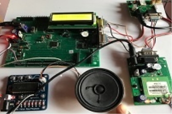 Fig 5(c):Wireless Black Box Modem
As shown in the above figure 5(c) this is the initial setup of the wireless blackbox wherein as the power supply is provided LPC 2148 Microcontroller is initiated along with the MEMS Accelerometer and voice playback Recorder .At the same time we also initiate power supply to the GPS Module and GSM Module and the LCD Module in LPC 2148 Microcontroller is kept in reset mode.
Fig 5(c):Wireless Black Box Modem
As shown in the above figure 5(c) this is the initial setup of the wireless blackbox wherein as the power supply is provided LPC 2148 Microcontroller is initiated along with the MEMS Accelerometer and voice playback Recorder .At the same time we also initiate power supply to the GPS Module and GSM Module and the LCD Module in LPC 2148 Microcontroller is kept in reset mode.
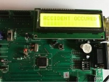 Fig 5(d):LCD Display when Accident Occured
As shown in the above figure 5(d) we can see a display message on LCD that accident occurred.
This message will appear on the LCD screen when a vehicle is under motion and if the vehicle undergoes unusual acceleration ,unusual vibrations due to any collision these mechanical moments are detected by the Mems Accelerometer and are converted to electrical signals and are given to the LPC 2148 Microcontroller that an accident occurred due to which the same is displayed on the LCD screen.
Fig 5(d):LCD Display when Accident Occured
As shown in the above figure 5(d) we can see a display message on LCD that accident occurred.
This message will appear on the LCD screen when a vehicle is under motion and if the vehicle undergoes unusual acceleration ,unusual vibrations due to any collision these mechanical moments are detected by the Mems Accelerometer and are converted to electrical signals and are given to the LPC 2148 Microcontroller that an accident occurred due to which the same is displayed on the LCD screen.
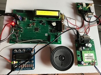 Fig 5(e):GPS Positioning on LCD when Accident Occured
As shown in above figure 5(e) when the moments of the mems accelerometer exceeds its reference voltage it is the indication that the accident occurred and it is displayed on the LCD i.e.,ACCIDENT OCCURRED.The LPC 2148 Microcontroller will provide this information to GPS system to obtain the Location of the vehicle where the accident occurred.As soon as the location is received by the LPC 2148 Microcontroller then this location information is sent to the recorded phone numbers i.e family members and nearest hospitals such that the location can be traced by the hospital staff so that voluntary services like treatment to the injured people can be provided on time to avoid many complications.There is also an advantage in this module such that the voices of the accident victims are recorded during the occurence of the accident so that the exact cause of the accident can be known later which will make it easy to find the evidences and causes for the occurences of the accident.
Fig 5(e):GPS Positioning on LCD when Accident Occured
As shown in above figure 5(e) when the moments of the mems accelerometer exceeds its reference voltage it is the indication that the accident occurred and it is displayed on the LCD i.e.,ACCIDENT OCCURRED.The LPC 2148 Microcontroller will provide this information to GPS system to obtain the Location of the vehicle where the accident occurred.As soon as the location is received by the LPC 2148 Microcontroller then this location information is sent to the recorded phone numbers i.e family members and nearest hospitals such that the location can be traced by the hospital staff so that voluntary services like treatment to the injured people can be provided on time to avoid many complications.There is also an advantage in this module such that the voices of the accident victims are recorded during the occurence of the accident so that the exact cause of the accident can be known later which will make it easy to find the evidences and causes for the occurences of the accident.
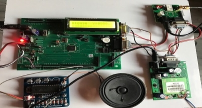 Fig 5(e):GPS Positioning on LCD when Accident Occured
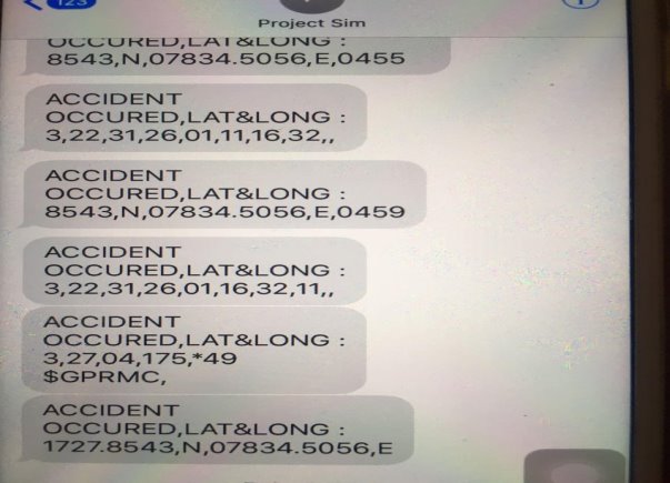 Fig 5(f):GPS Positioning Messages Sent to Mobile Phones using GSM
As shown in the above figure we can see the latitude,longitude information of the accident spot.whenevermems accelerometer exceeds the threshold voltage it sends the corresponding latitude,longitude information of the place by using GPS to track information and there by sending message to the near and dear persons related to that person who is involved in accident and it also sends the message to the nearest hospitals to accident spot by using GSM
5.4 CONCLUSION:
Accident in motorcycle are mainly divided into two groups including fall by themselves and crash by other objects. Thus, the device may be tested with a limited number of situations of accidents. By implementation of this project it will be in great help to the accident victims for the detection and location of accident spot to the emergency services like hospitals and police stations to get emergency services that will help the accident victims in recovery .Even the voices of the accident victims are recorded during the occurrence of the accident which is helpful for the detection of the reasons of occurring of accident .The location of the accident spot is located by the GPS module and is sent to the nearest emergency services with the help of GSM module. Due to this emergency services can be done in time which will reduce the damage to some extent. Therefore wireless black box with mems accelerometer will be in great help for accident detection and location of the spot along with the provision of emergency services.
Fig 5(f):GPS Positioning Messages Sent to Mobile Phones using GSM
As shown in the above figure we can see the latitude,longitude information of the accident spot.whenevermems accelerometer exceeds the threshold voltage it sends the corresponding latitude,longitude information of the place by using GPS to track information and there by sending message to the near and dear persons related to that person who is involved in accident and it also sends the message to the nearest hospitals to accident spot by using GSM
5.4 CONCLUSION:
Accident in motorcycle are mainly divided into two groups including fall by themselves and crash by other objects. Thus, the device may be tested with a limited number of situations of accidents. By implementation of this project it will be in great help to the accident victims for the detection and location of accident spot to the emergency services like hospitals and police stations to get emergency services that will help the accident victims in recovery .Even the voices of the accident victims are recorded during the occurrence of the accident which is helpful for the detection of the reasons of occurring of accident .The location of the accident spot is located by the GPS module and is sent to the nearest emergency services with the help of GSM module. Due to this emergency services can be done in time which will reduce the damage to some extent. Therefore wireless black box with mems accelerometer will be in great help for accident detection and location of the spot along with the provision of emergency services.
Fig 5(c):Wireless Black Box Modem
As shown in the above figure 5(c) this is the initial setup of the wireless blackbox wherein as the power supply is provided LPC 2148 Microcontroller is initiated along with the MEMS Accelerometer and voice playback Recorder .At the same time we also initiate power supply to the GPS Module and GSM Module and the LCD Module in LPC 2148 Microcontroller is kept in reset mode.
Fig 5(d):LCD Display when Accident Occured
As shown in the above figure 5(d) we can see a display message on LCD that accident occurred.
This message will appear on the LCD screen when a vehicle is under motion and if the vehicle undergoes unusual acceleration ,unusual vibrations due to any collision these mechanical moments are detected by the Mems Accelerometer and are converted to electrical signals and are given to the LPC 2148 Microcontroller that an accident occurred due to which the same is displayed on the LCD screen.
Fig 5(e):GPS Positioning on LCD when Accident Occured
As shown in above figure 5(e) when the moments of the mems accelerometer exceeds its reference voltage it is the indication that the accident occurred and it is displayed on the LCD i.e.,ACCIDENT OCCURRED.The LPC 2148 Microcontroller will provide this information to GPS system to obtain the Location of the vehicle where the accident occurred.As soon as the location is received by the LPC 2148 Microcontroller then this location information is sent to the recorded phone numbers i.e family members and nearest hospitals such that the location can be traced by the hospital staff so that voluntary services like treatment to the injured people can be provided on time to avoid many complications.There is also an advantage in this module such that the voices of the accident victims are recorded during the occurence of the accident so that the exact cause of the accident can be known later which will make it easy to find the evidences and causes for the occurences of the accident.
Fig 5(e):GPS Positioning on LCD when Accident Occured
Fig 5(f):GPS Positioning Messages Sent to Mobile Phones using GSM
As shown in the above figure we can see the latitude,longitude information of the accident spot.whenevermems accelerometer exceeds the threshold voltage it sends the corresponding latitude,longitude information of the place by using GPS to track information and there by sending message to the near and dear persons related to that person who is involved in accident and it also sends the message to the nearest hospitals to accident spot by using GSM
5.4 CONCLUSION:
Accident in motorcycle are mainly divided into two groups including fall by themselves and crash by other objects. Thus, the device may be tested with a limited number of situations of accidents. By implementation of this project it will be in great help to the accident victims for the detection and location of accident spot to the emergency services like hospitals and police stations to get emergency services that will help the accident victims in recovery .Even the voices of the accident victims are recorded during the occurrence of the accident which is helpful for the detection of the reasons of occurring of accident .The location of the accident spot is located by the GPS module and is sent to the nearest emergency services with the help of GSM module. Due to this emergency services can be done in time which will reduce the damage to some extent. Therefore wireless black box with mems accelerometer will be in great help for accident detection and location of the spot along with the provision of emergency services.
CHAPTER 6
FUTURE SCOPE
- Development of smarter vehicles applications. These can be developed by using a controller module such that it will be taking photograph of the accident spot so that tracking is easier.
- By applying ultrasonic sensors features we can detect the distance of a vehicles moving nearby our vehicles.
- Introducing satellite phones in place of GSM modules for more effective signal transmission in case of week signals.
- This system can be interfaced with vehicle airbag system that prevents vehicle occupants from striking interior objects such as steering wheel or window.
Cite This Work
To export a reference to this article please select a referencing stye below:
Reference Copied to Clipboard.
Reference Copied to Clipboard.
Reference Copied to Clipboard.
Reference Copied to Clipboard.
Reference Copied to Clipboard.
Reference Copied to Clipboard.
Reference Copied to Clipboard.
Related Services
View all


Related Content
All TagsContent relating to: "Engineering"
Engineering is the application of scientific principles and mathematics to designing and building of structures, such as bridges or buildings, roads, machines etc. and includes a range of specialised fields.
Related Articles

DMCA / Removal Request
If you are the original writer of this dissertation and no longer wish to have your work published on the UKDiss.com website then please: